I. INTRODUCTION
In the past few years, we have witnessed a growing amount of Ka-band capacity launched in many regions of the world. Fuelled by the growth of bandwidth hungry applications, the demand for satellite capacity has grown similar to other wire line and wireless communications technologies [Reference Singarajah1].
Considering the scope of transmission at Ka-band, this paper is devoted to the design and development of carrier generator using phase-locked loop (PLL) frequency synthesizer at Ka-band for Indian remote sensing (IRS) applications.
The modern technology of frequency synthesis has been classified into three main categories. They are direct synthesis (DS), digital direct synthesis (DDS), and PLL frequency synthesis. DS has excellent performance in terms of short frequency switching time, but it consumes more power as it needs to integrate filter, mixer, etc. DDS can provide high-resolution and low-phase noise signals, but it has limited operating range and shows weak spurious suppression. PLL synthesizer has a wide output range and a great suppression of spurious frequencies. A PLL design can be integer (N)-based PLL or fractional (F)-based PLL.
In this paper, integer N-type PLL frequency synthesis structure is proposed and implemented. The main idea is to generate X-band carrier signal using PLL frequency synthesizer [Reference Wang, Lin and Wang2, Reference Pandit, Chitra, Basu and Ingale3] and multiply it to Ka-band signal using a frequency tripler [Reference Yuk, Wong and Branner4]. The output of the X-band carrier generator is fed to the frequency multiplier with the multiplication factor (N = 3) generating a signal at Ka-band.
The implemented model has excellent performance with resolution of 5.7 MHz, output at Ka-band and phase noise better than −70 dBc/Hz at 1 kHz offset. The measured result for Ka-band carrier phase noise matches with the theoretical values, as described later in this paper.
II. WORKING PRINCIPLE
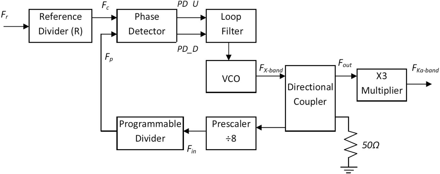
The block diagram of the PLL frequency synthesizer is shown in Fig. 1. The PLL compares the phase between the signal F p obtained by dividing the frequency of voltage-controlled oscillator (VCO) by Prescaler and programmable divider and F c obtained by dividing the reference frequency F r, and generates a phase error signal which is applied to the VCO through a loop filter to control the output frequency of VCO. This continues till the loop gets looked, i.e., VCO gets locked to the frequency and phase of temperature compensated crystal oscillator (TCXO). The frequency resolution is given by equation (1).
 $$F_c=F_r \div \lpar R+1\rpar.$$
Fig. 1. Block diagram of N-type PLL frequency synthesizer.
The highly stable reference signal (F r) of PLL is given by a TCXO. The phase detector input F p is derived by equation (2)
 $$F_P=F_{{\rm in}} \div [10 (M+1) +A ] \comma \;$$
where M and A are the counter values. The output signal from the VCO is fed to the divide by-8 prescaler. This output frequency F in is given by equation (3)
 $$F_{{\rm in}}= [10 (M+1) +A ] \times [Fr \div (R+1)].$$
In the locked condition both equation (1) and (2) must be satisfied. After generating X-band carrier frequency, the output is fed to frequency tripler to generate carrier at Ka-band.
III. CIRCUIT IMPLEMENTATION
The described analysis in Section II is used to realize X-band frequency synthesizer and frequency tripler. The circuit design is described in the following parts:
A) Part A
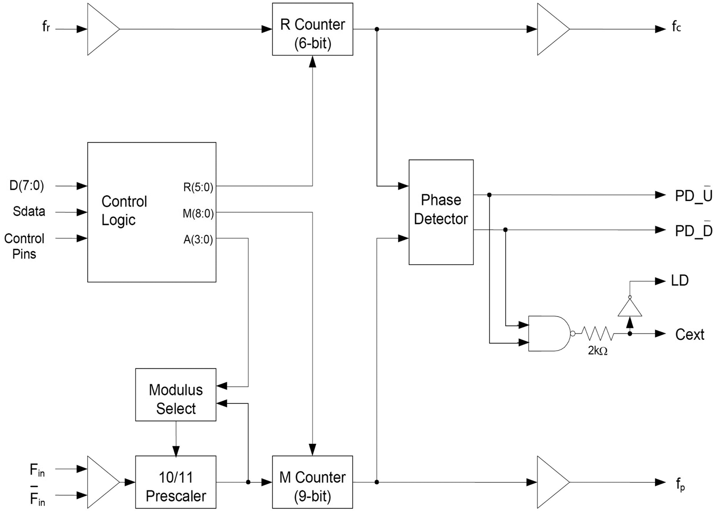
Peregrine's PE83336, a high-performance integer-N PLL chip capable of frequency synthesis up to 3.0 GHz is used. The PE83336 consists of a prescaler, counters, a phase detector, and control logic as shown in Fig. 2. The dual-modulus prescaler divides the VCO frequency by either 10 or 11, depending on the value of the modulus select. Counters “R” and “M” divide the reference and F in, respectively, by integer values stored in a 20-bit register. An additional counter (“A”) is used in the modulus select logic. The phase frequency detector generates up and down frequency control signals. The control logic includes a selectable chip interface. Data can be written via serial bus, parallel bus, or hardwired direct to the pins.
Fig. 2. Functional block diagram of PE83336 IC.
The stable reference frequency is given by TCXO. The circuit realization using PE83336 is shown in Fig. 3.
Fig. 3. Circuit realization of phase detector.
B) Part B
Figure 4 represents the active loop filter used in conjunction with the differential output of the PE83336 phase detector. Since all the parameters of PLL are fixed and specific to the components used, the loop filter is the only block that gives a degree of freedom with regard to the design of the PLL, in terms of close-in phase noise characteristics and the lock time. The ideal values of resistor and capacitor in loop filter are gotten from the simulation carried out on Agilent Systemvue software.
Fig. 4. Circuit realization of loop filter.
The loop bandwidth is chosen such that the phase noise transition from TCXO to VCO is smooth. It is well known that the phase noise inside the loop bandwidth follows the TCXO phase noise multiplied by 20 × log (VCO operating frequency/TCXO operating frequency) and that outside the loop, follows the VCO phase noise. The loop bandwidth of 50 kHz is chosen in our application.
C) Part C
A Teledyne Cougar OAS 8900 VCO with the tuning range of 6900 to 8900 MHz is shown in Fig. 5. The output of the VCO (OAS 8900) is fed back to the PLL IC (PE83336) through a 10-dB coupler and a Divide-by-8 prescaler, so that L-band signal reaches the F in of the PLL IC.
Fig. 5. Circuit realization of VCO and prescaler.
D) Part D
TriQuint TG4040 with an operating band of 17–43 GHz is used for performing frequency multiplication. TG4040 is a medium power amplifier and a multiplier. The part has been developed by TriQuint using its 0.15 um power pHEMT production process. It provides a nominal 25 dB small signal gain with 22 dBm output power at 1 dB gain compression. For X3 Multiplier Function, TGA4040 provides 15 dBm typical Output Power at 9 dBm Pin. The TGA4040 is 100% DC and RF tested on-wafer to ensure performance compliance.
IV. TESTING AND HARDWARE REALIZATION
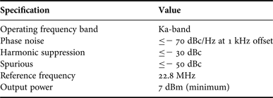
The design of the Ka-band frequency synthesizer consists of the X-band carrier generator as the first circuit followed by a frequency multiplier. The main technical requirements of the frequency synthesizer are given in Table 1.
Table 1. Desired specification.
The phase noise of the X-band carrier deteriorates from the phase noise of TCXO at 22.8 MHz due to the multiplication effect and can be calculated from equation (4).
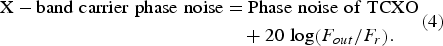 $$\eqalign{{\rm X - band}\, \, {\rm carrier}\, \, {\rm phase}\, \, {\rm noise} & = {\rm Phase}\, \, {\rm noise}\, \, {\rm of}\, \, {\rm TCXO } \cr & \quad +20\, \, {\rm log}{\left(F_{out} /F_r \right)}.}$$
The phase noise value of the TCXO is taken from Fig. 6. The X-band carrier phase noise is calculated from (4) and compared to that obtained practically from Fig. 7. The X-band carrier phase noise is −82 dBc/H at 1 kHz offset.
Fig. 6. Phase noise of TCXO.
Fig. 7. Phase noise of PLL at X-band.
The output of the X-band PLL is multiplied by a frequency tripler and driven through driver amplifier. The minimum phase noise degradation, caused by an ideal frequency multiplier is:
 $${\rm Phase}\, \, {\rm noise}\, \, {\rm degradation}=20 \times LOG\left(N \right)\comma \;$$
where N is the multiplication factor [Reference Brennan5]. Thus, a frequency tripler (N = 3) degrades phase noise by at least 9.5 dB. The phase noise of X-band carrier is: −82 dBc/Hz at 1 kHz offset. Using a multiplier (N = 3), degrades this phase noise by 20 × LOG (3) = 9.5 dB, yielding: −82 dBc/Hz + 9.5 dB = −72.5 dBc/Hz at 1 kHz offset at Ka-band. Both X-band carrier and Ka-band carrier phase noises are measured, agreeing with the theoretical estimated phase noise.
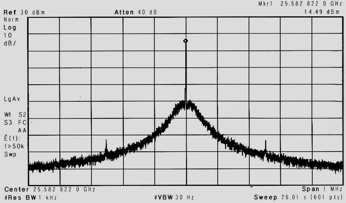
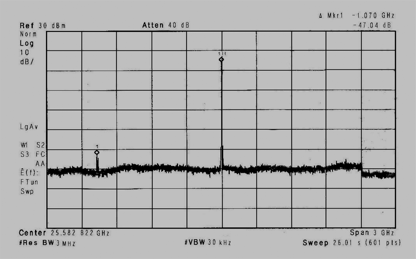
Figures 8 and 9 show the spectrum of the frequency synthesizer output at Ka-band. A spurious of −47 dBc is observed, as seen in Fig. 9, at an offset of 1070 MHz from the carrier, which marginally misses the desired spurious level of −50 dBc or lesser. Hence, an additional bandpass at Ka-band is required, which would provide an attenuation of at least 3 dB at the spurious frequency. Also the phase noise of −70 dBc/Hz at 1 kHz is obtained as seen in Fig. 8, satisfying the theoretical phase noise.
Fig. 8. Frequency synthesizer output at Ka-band for measuring phase noise.
Fig. 9. Frequency synthesizer output at Ka-band showing the spectral purity
V. CONCLUSION
In this paper, Ka-band frequency synthesizer with PE83336 chip on RT-duroid 6010 substrate is implemented. The proposed model provides an excellent flexibility of carrier generation at both X- and Ka-band frequencies (Figs 10 and 11). The flexibility for changing the frequency at X-band is obtained by the ability to change any of the counter values. The carrier generator achieves the frequency resolution of 5.7 MHz, and phase noise better than −70 dBc/Hz at 1 kHz offset at Ka-band is achieved.
Fig. 10. Top view of fabricated X-band carrier generator on RT-duroid 6010 substrate.
Fig. 11. Top view of X-band carrier generator with X3 multiplier and driver amplifier.
ACKNOWLEDGEMENT
The author expresses sincere gratitude to Sri Ranganath Ekkundi Dy. Director, CPA & Sri Yateendra Mehta, Group Director, CMG at ISRO Satellite Centre for their valuable guidance, encouragement, and support. The authors sincerely acknowledge Sri K. Chandrashekar, Program Head, DSP/RF (CET) & Dr. Krishna Venkatesh, Director, Centre for Emerging Technologies, Jain University, Bangalore, for their valuable guidance and support.
 Vabya Kumar Pandit is a final year M.Tech., Scholar at the Centre for Emerging Technologies, Jain University, Bangalore, in the area of Radio Frequency Communication. He completed B.E. in Electronics and Tele-Communications Engineering, from Chhattisgarh Swami Vivekananda Technical University (CSVTU), Bhilai in the year 2011. His research interests include microwave and millimeter-wave passive and active circuit design, planar miniaturized filter design, etc. He has published two papers in international journals.
 Chitra R. completed her Bachelor's degree from Madras University in 1980 and her Master's degree from the Indian Institute of Science, Bangalore in 1990. She has been quite instrumental in the development of Data Transmitters for Remote sensing and Geostationary spacecrafts at ISRO Satellite Centre. Currently, she is heading the Data Transmitter and Navigation Division of Communication Systems Group at ISRO Satellite Centre, Bangalore, India. She has published more than six papers in national and international conferences/journals.
 Sourabh Basu completed his Bachelor's degree in Electronic Science from Delhi University in 2001 & his Masters in Microwave Electronics from Department of Electronic Science, University of Delhi in the year 2005. Currently, he is working as a Scientist/Engineer in Data Transmitter and Navigation Division of Communication Systems Group at ISRO Satellite Centre, Bangalore, India.
 Deepak V. Ingale completed his M.Tech. in VLSI and Embedded Systems in 2008. Currently, he is working as an Assistant Professor at the Centre for Emerging Technologies, Jain University, Bangalore, India. As a Project Engineer at Wipro Technologies he was instrumental in component selection, board re-design (PCB), setting up & conducting First Piece Evaluation (FPE) of various telecom switches and related activities. He has more than four papers to his credit which got published in national and international conferences/symposiums.