


I. INTRODUCTION
Wireless technology has been evolving from cellular to wireless broadband and to personal area network applications. As can be already seen in today's 3G voice/data Systems, users may be moving while simultaneously operating in multimedia streaming sessions or in a broadband data access [Reference Steer1]. To interact with a multi-services network, radio technology should change between an operative band to another and adapting its features according to the different available standards. To this aim, multi-band radio technologies have been extensively addressed by several research projects and covered by the scientific literature [Reference McCune2]. Despite these efforts, presently there is no optimum multi-band radio topology. Basic system-level solutions are referred to as a software-defined radio (SDR), a radio communication system that uses software for the reconfiguration of the digital or analogue part of the sub-system for the modulation and demodulation of the radio signals [Reference Abidi3]. Most of the systems in the market still support only a very limited number of standards (e.g. Global System for Mobile Communications (GSM), Universal Mobile Telecommunications System (UMTS) and, when available, Bluetooth). Further communication standards are supposed to enter the market in the near future, and, if possible, they can be used without hardware modifications. The RF transmitter power amplifier (PA) will be a key point of this chain. Today, dedicated PAs achieve very good power added efficiency (PAE) and, as a consequence, long battery lifetime. Any reconfigurable PA, needed for the support of different, not always predefined, communication systems, must compete with these dedicated solutions. Flexible receivers for either multi-band or SDR have been investigated in this field and this paper deals with the evaluation of a low-cost new PA design methodology to be considered as an enabling sub-system for the above-described scenario.
The paper is organized as follows: An overview of the state-of-the-art multi-band PA architectures will be given in Section II, highlighting the advantages and weaknesses for each topology. The PA prototype design methodology and its experimental characterization are described in Section III, while the PA system-level analysis is reported in Section IV. Conclusions are finally drawn in Section V.
II. MULTI-BAND PA ARCHITECTURES
Multi-band PA strategies can be roughly divided into three main approaches (see Figs 1–3). The most straightforward solution is to use two dedicated PAs coupled by a diplexer, designed to separate the two spectra according to the required communication standards (Fig. 1). The PAs operate at their respective carrier frequencies. The isolation is assured by a diplexer, which could represent a critical issue in case of closer operative spectrum bands. The loss introduced by this diplexer typically is in the range of a few dBs, thus determining a reduction of the resulting overall system performance, in particular at the output stage. For quick product development this solution appears very interesting, but it represents a not optimized solution in terms of costs and performance. A second approach (see Fig. 2) consists in employing tunable/switching components in the matching networks, to enable the capability coping with more than one standard. In this solution, usually referred to as adaptive PA, the efficiency is also enhanced (see e.g. [Reference Neo4]), selecting the proper termination for each power level. The main drawback of this solution, in principle very flexible and suitable for the implementation of software-based controlled subsystems, is related to the losses exhibited by tunable components such as the needed variable capacitors or tunable inductors, affecting the overall system features. Another critical point is represented by the solid-state devices normally included in the matching networks to enable parameter tuning, which introduce linearity constraints. The third approach consists in the so-called concurrent PA, or, in other words, in a system able to simultaneously operate in different bands (Fig. 3). In this case the matching networks are designed to maximize device performances, allowing simultaneous operability in all bands, while avoiding the use of switches or reconfigurable elements and pertinent control voltages (see e.g. [Reference Hashemi and Hajimiri5]). In this case, the most critical point is clearly represented by the matching networks constraints since they have to be able to synthesize the device optimum loads at different frequencies. The aim of this paper is to study, investigate, and evaluate the feasibility of a dual-band power amplifier using low-cost HBT SiGe technology. For this purpose, the concurrent approach (Fig. 3) has been selected since it is the only one that allows simultaneous interoperability in the selected working bands.

Fig. 1. Schematic of combined PAs.

Fig. 2. Schematic of adaptive PA.

Fig. 3. Schematic of the dual-band PA.
III. PA DESIGN
In order to investigate the features of a concurrent topology, a PA has been developed based on a new SiGe BiCMOS active device, provided by the IHP foundry [Reference Knoll6, Reference Knoll7], to operate at frequencies of 2.45 and 3.5-GHz. Accounting for technology novelty and the lack of device characterization and modeling, a hybrid (MIC) approach was adopted for fast prototyping and in order to evaluate device potentiality also. In particular, the following steps were adopted:
– characterization of the active device under small and large signal conditions;
– design of the matching network;
– integration of the PA prototype and tests.
The prototype developed was realized by designing matching networks on a low-cost plastic substrate (TACONIC CER-10) and connecting such nets to the active device through wafer probes, as schematically depicted in Fig. 4.

Fig. 4. Hybrid (MIC) PA prototype.
A) Active device characterization
The active device was extensively characterized in both linear and nonlinear regimes. Figure 5 shows an HBT cross section. Since the DUT is an HBT device, for the static I–V output characteristics the collector to emitter voltage V CE was varied in the range from 0 to 8.5-V, while the base current I B was varied from 20-μA to 1.4-mA. The resulting measured I–V characteristics are reported in Fig. 6. Following that, scattering parameter measurements were performed for different bias points, in the range 100-MHz–40-GHz. Accounting for the DC curve for the design of the PA, the bias point V CE = 4.5-V and I B = 0.4-mA was chosen. According to this bias point, Figs 7 and 8 report the corresponding S-parameter behavior in terms of input (S 11) and output (S 22) reflection coefficient and small signal gain (S 21), referred to the DUT reference planes highlighted in Fig. 4. Successively, nonlinear characterization was performed for the design frequencies of 2.45 and 3.5-GHz, with an active harmonic load-pull test bench based on the active loop approach [Reference Ferrero and Pisani8]. The measured optimum fundamental termination from load-pull maps at 2.45-GHz, at 3-dB of gain compression, was ΓL,f1 = |0.4|e j114°, showing an output power, and PAE of 19.6-dBm and 39%, respectively (see Fig. 9). The measured DUT input reflection coefficient was Γin,f1 = |0.83|e −j179°. For the same bias conditions and compression, at 3.5-GHz the identified optimum load was ΓL,f2 = |0.52|e j104°, while the DUT input reflection coefficient was Γin,f2 = |0.91|e − j177°, showing an output power of 19.5-dBm and a PAE of 40% (Fig. 10). As can be noted, the two sets of curves, at 2.45 and 3.5-GHz respectively, exhibit pretty similar figures in terms of output power, PAE, and gain.

Fig. 5. HBT cross section.

Fig. 6. Static device DC characteristics.

Fig. 7. Scattering parameter S 11 and S 22 for the DUT in the bias point V CE = 4.5-V and I B = 0.4-mA selected for the PA design.

Fig. 8. Small signal gain S 21 for the DUT in the bias point V CE = 4.5-V and I B = 0.4-mA selected for the PA design.

Fig. 9. Power sweep on optimum load (ΓL, f1) at the fundamental frequency of 2.45-GHz.

Fig. 10. Power sweep on optimum load (ΓL, f2) at the fundamental frequency of 3.5-GHz.
B) PA design
In order to realize the PA prototype, the idea was to design the input and output matching networks to fulfill, across the DUT reference sections (see Fig. 4), the optimum loading condition previously reported. For this purpose, it was required to properly de-embed the contribution of SMAs and probes used to connect the nets to the DUT and the rest of the set-up. The matching networks were designed by using a lumped/distributed approach and following the criteria reported in [Reference Colantonio, Giannini, Giofrè and Piazzon9, Reference Colantonio, Giannini and Scucchia10]. The impedance transformation required for the output matching network (OMN) was realized by the scheme shown in Fig. 11, where the impedance transformations realized in each section are also represented. Accounting for the measured S-parameter of the output probing connections, the optimum loads ΓL, f1 and ΓL, f2 to be synthesized in Section A have been de-embedded to obtain the load condition to be fulfilled in Section B. The resulting network transformation from the external 50-Ω termination up to Section B is reported in Fig. 11. A similar procedure was adopted for the design of the input matching network (IMN) to fulfill the conjugate matching conditions represented by the two source reflection coefficients Γs,f1 = |0.83| expj179° and Γs,f2 = |0.91| expj177°, respectively. The input network scheme is reported in Fig. 12, together with the loading transformation performed in each section. The pictures of the realized matching networks are reported in Figs 13 and 14, respectively.

Fig. 11. Output matching network.

Fig. 12. Output matching network.

Fig. 13. Picture of PA input matching network.

Fig. 14. Picture of PA output matching network.
C) PA characterization
In order to experimentally evaluate the performance of the whole test system, the PA was measured both in small signal (SS) scattering parameters and in large signal (CW) power measurements at the two fundamental frequencies of interest. Figure 15 shows the measured transmission S 21 and matching S 11 scattering parameter of the amplifier. As expected for this preliminary test structure, the hybrid setup implemented (see Fig. 4) deeply affects the performance of the amplifier, in terms of both absolute gain and actual working frequencies.

Fig. 15. Measured transmission S 21 and matching S 11 scattering parameters of the amplifier.
For the former, the losses introduced by the matching nets have been estimated to be of the order of 1 and 0.6-dB for IMN and OMN, respectively. For the absolute gain, an actual frequency shift was observed, which was partially compensated through additional delay elements properly tuned during measuremens. Nevertheless, a non-negligible mismatch at the prototype input was experimentally verified, which implies a power gain reduction of the realized PA with respect to the load-pull measurements on the DUT. As a result, the SS gains in the two bands are roughly 12-dB at 2.575-GHz and 9-dB at 3.4-GHz. Figures 16 and 17 show output power, power gain, and power added efficiency (PAE) vs. input power (P in) at 2.575 and 3.4-GHz (maximum of the SS gain), respectively. As can be clearly seen, output power is around 17.5-dBm, gain is near 10-dB, and PAE is close to 20% for both the frequencies. The effect of the setup is also evident from power performance, resulting in roughly 2-dB of output power losses with respect to the stand-alone DUT performance, which could be alleviated in an MMIC realization.

Fig. 16. Output power, power gain, and PAE vs. input power (P in) at the fundamental frequency of 2.575-GHz.

Fig. 17. Output power, power gain, and PAE vs. input power (P in) at the fundamental frequency of 3.4-GHz.
IV. SYSTEM-LEVEL ANALYSIS
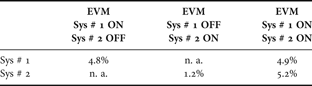
While the above discussion highlighted the design methodology for dual-band concurrent PA, this section describes its potentiality when implemented in SiGe-MMIC technology and involved in a possible scenario for the next generation of wireless communication. For this purpose, a complete schematic of such a PA was designed following the design rule and completed with all the parts required for its full functioning, which are biasing networks input/output matching networks, stabilizing network, and ballast network. In addition, a CAD platform was adopted to simulate PA behavior when dealing with concurrent dual-band modulated signals. The system was implemented in the Agilent-ADS suite by using behavioral models for the mixers and signal sources, while the two base-band signals were implemented by using the physical layer defined for the OFDM-IEEE 802.16e signal and specifically the 20-MHz bandwidth, 64 QAM mode. A dual-band concurrent transmitter architecture based on the double-image rejection scheme was implemented. This solution, in addition to effective image suppression, enables the capability to simultaneously up-convert two baseband signals around the desired carrier frequencies. The system was co-simulated using the data-flow and envelope engines. The complete design in IC technology has led to a dual-band PA frequency behavior with power gains at two frequency bands of 2.45 and 3.4-GHz which differ from those reported in Figs 9 and 10. This is mainly due to the additional element considered in the circuit, which determines increased losses, and overall a low-pass behavior, which makes the higher operative frequency much more affected than the lower. As a consequence, a larger difference is observed between the two operative frequencies than in the previous discussed experimental results. The system-level analysis firstly considers the effects of the in-band and the out-of-band distortion of a two-tone excitation. An envelope analysis is required to investigate spectral re-growth and modulation integrity, although a significant effect is due to cross-modulation between the two envelopes. To take into account this higher order of complexity, the numerical resources required increase considerably when compared to single carrier–single enveloped analysis. Figure 18 provides a comparison between the response at fundamental for the concurrent dual-band PA when driven by a single-tone and by a two-tone signal. Three simulations have been carried out, the first considering the single-tone excitation at 2.45-GHz, the second considering the single-tone excitation at 3.5-GHz, and, finally, the third considering the simultaneously two-tone excitation; the power level ranges have been kept constant through the simulations. From Fig. 18 it is possible to observe that for the low-level injection the two sets of curves converge to the small signal, while on increasing the power of the single-tone excitation, the corresponding responses exhibit an input referred to 1-dB compression of −5 and 0-dBm at 2.45 and 3.5-GHz, respectively. The higher value of compression for the higher band is mainly due to the reduced gain exhibited by the PA at this frequency. When considering the concurrent excitation, the input power level at which the gain decreases by 1-dB reduces sensibly with respect to the single-mode operation. In particular, we observed a reduction of approximately 3-dB for the lower band and 7-dB for the higher band, due to the different gain figures exhibited by the PA, causing a change in the dynamic load lines, in a way very similar to typical mixer operation. The power levels for the two digitally modulated signals were fixed in order to hold, in the concurrent dual-band operative conditions, the maximum EVM within 5%. These values result in output power levels of 11 and 3.5-dBm, respectively, at 2.45 and 3.5-GHz. That value of EVM is typical for system communication requirements involving OFDM broadband signals, e.g. WLAN or WiMAX. The analysis results of the EVM in the three different operative conditions are reported in Table 1 for 11 and 3.5-dBm, respectively, for lower and higher frequency. In the table, System # 1 refers to the modulated signal with center band at 2.45-GHz and System # 2 to the one at 3.5-GHz. As can be noted from the table, System # 1 does not improve its figure sensibly, while System # 2 exhibits a significant reduction of the EVM from 5.2 to 1.2%, moving from the concurrent to the single-band operation mode. A different point of view of these results is achieved observing the spectra for concurrent and single-system operations. With reference to Figs 19 and 20, it is possible to clearly observe modification of the PA output spectrum in the two bands and for the two different operations. While the integrated power for the two systems does not change considerably, moving from single systems to concurrent systems, the gain flatness and the out-of-band spectrum change significantly only for the 3.5-GHz system. This is a result consistent with the EVM figures reported in Table 1 and with the compression characteristic reported in Fig. 18, providing better insight into the operation of the dual-band PA.

Fig. 18. Gain comparison of the large-signal single-tone and two-tone analyses of the concurrent dual-band PA.

Fig. 19. Comparison between spectra at 2.45-GHz in single-system operation (bottom figure) and in the presence of a concurrent system at 3.5-GHz (top figure). The graphs also report the large signal gain of the PA.

Fig. 20. Comparison between spectra at 3.5-GHz in the single-system operation (bottom figure) and in the presence of a concurrent system at 2.45-GHz (top figure). The graphs also report the large signal gain of the PA.
Table 1. EVM calculation for the dual-band PA.
V. CONCLUSIONS
This paper has dealt with the design of a concurrent low-cost dual-band PA fabricated in SiGe technology and its system-level investigation. A hybrid MIC approach has been adopted both for a fast prototyping of the PA and for the evaluation of the device potentiality based on an extensive linear and nonlinear characterization. This has permitted the design of matching networks in order to optimize their behavior at 2.45 and 3.5-GHz. The measured PA prototype has shown output powers of 17.2 and 17-dBm at a 1-dB compression point, at 2.45 and 3.5-GHz, respectively, for CW single-mode operation, with a PAE around 20%. Nevertheless, the dual-band PA design methodology presented here and its investigation at system level highlighted new concepts and possible system architecture solutions for the development of the next generation of a multi-band transceiver front-end.
ACKNOWLEDGEMENTS
The research reported here was performed in the context of the networks TARGET “Top Amplifier Research Groups in a European Team” supported by the Information Society Technologies Programme of the EU under contract IST-1-507893-NOE, www.target-net.org and NEWCOM++ supported by the Seventh Framewok Programme Theme n.ICT-1-1.1. The authors also wish to thank R. Scholz and D. Knoll from IHP for providing the active devices.
 Vittorio Camarchia was born in Turin, Italy, in 1972. He received the Laurea degree and Ph.D. degree in electronic engineering from the Politecnico di Torino, Turin, Italy, in 2000 and 2003, respectively. In 2001, 2002, and 2003, he was a Visiting Researcher with the Electrical and Computer Engineering Department, Boston University. In February 2003, he joined the Dipartimento di Elettronica, Politecnico di Torino. His research is focused on RF device modeling, simulation, and characterization, both linear and nonlinear. Dr. Camarchia was the recipient of the 2002 Young Graduate Research Fellowship presented by the Gallium Arsenide Application Symposium (GAAS) Association. He is a member of the Editorial Board of the IEEE MTT Transactions.
 Rocco Giofrè was born in Vibo Valentia (Italy) on 13 August 1979 and received the electronic engineering degree (M.S. Eng.), summa cum laude, from University of Roma Tor Vergata in 2004. He is currently working toward a Ph.D. degree in Space Systems and Technologies at the same university. His current research interests include RF power amplifier theory, design and test, linearization techniques, and efficiency improving techniques. He was recipient of the 2005 Young Graduate Research Fellowship presented by the Gallium Arsenide Application Symposium Association (GAAS) and of the best paper award at the 2nd EuMIC Conference in 2007.
 Iacopo Magrini received the Laurea and Ph.D. degrees in electronics from the University of Florence in 2001 and 2005, respectively. In 2001 he joined the staff of Microelectronic Laboratory (Department of Electronics and Telecommunications) at University of Florence. In 2002, within the framework of Ph.D. activities, he was at Philips Semiconductor. After the Ph.D., he received a grant from University of Florence as a post-doc. His main research activities include system-level simulations along with MMIC design for wireless applications. Starting from 2003 he joined, as a researcher, NoE-TARGET, whose topic is mainly focused on the development of multi-band multi-standard transceivers for handset applications. Dr. Magrini has also been involved in several consulting tasks for the development of advanced circuits oriented to industrial and space applications.
 Luca Piazzon was born in Frascati, Italy, in 1982. He received his B.S. degree in electronic engineering from Tor Vergata University, Rome, Italy, in 2007. Currently, from November 2008, he is a Ph.D. student at the Tor Vergata University. His current research interests include RF power amplifier theory, design and test, linearization techniques, and efficiency improving methodologies.
 Alessandro Cidronali received the Laurea and Ph.D. degrees in electronics engineering from the University of Florence, Florence, Italy, in 1992 and 1998, respectively. In 1993, he joined the Department of Electronics Engineering, University of Florence, where he became an Assistant Professor in 1999, and where he teaches “Electron Devices” and “Integrated Microwave Circuits”. His research activities cover the study of circuits and system architectures enabling new wideband transmitters, the design of broadband MMICs, and the development of CAD and numerical modeling for microwave devices and circuits. He was Visiting Researcher at the Motorola Physics Science Research Lab from 1999 to 2003 and Guest Researcher at National Institute of Standards and Technology (NIST), Electromagnetic Division, Non-Linear Device Characterization Group, from 2002 to 2005. In the frame of the EU Network TARGET – “Top Amplifier Research Groups in a European Team”, he served as Workpackage Leader for the ‘Multiband transmitters modeling and design for wireless broadband access’ workpackages. He was recipient of the best paper award at the 61th ARFTG Conference. From 2004 to 2006 Dr. Cidronali served as an associate editor for the IEEE Transactions on Microwave Theory and Techniques.
 Paolo Colantonio was born in Roma, Italy on March 22, 1969. He received the degree in electronic engineering from University of Roma Tor Vergata in 1994 and the Ph.D. degree in microelectronics and telecommunications in 2000. In 1999 he became a Research Assistant at the same university, where since 2002 he has been a Professor of Microwave Electronics. His main research activities are in the field of nonlinear microwave circuit design methodologies, nonlinear analysis techniques, and modeling of microwave active devices.
 Simona Donati Guerrieri was born in 1969 in Milano, Italy. She received a degree in theoretical physics in 1993 from University of Milano and her Ph.D. in Electron Devices from University of Trento in 1999. In 1998 and 2000 she was with the ULSI Technology Research Department of Bell Labs as a consultant, working on physics-based noise modeling of electron devices. She is presently a researcher in the Electronics Department of Politecnico of Torino. Her research interests include the modeling and simulation of microwave solid state devices, and RF and microwave integrated circuit design.
 Giovanni Ghione was born in 1956 in Alessandria, Italy. He graduated cum laude in electronic engineering from Politecnico di Torino in 1981. In 1990 he joined the University of Catania as Full Professor of Electronics, and from 1991 he was again with Politecnico di Torino. His present research interests concern the physics-based simulation of active microwave and optoelectronic devices, with particular attention to noise and thermal modeling. He is a member of the Editorial Board of the IEEE MTT Transactions.
 Franco Giannini was born in Galatina (LE) Italy, on 9 November 1944. He received the degree in electronics engineering, summa cum laude, in 1968, and in 2008 he was awarded the Laurea Honoris Causa Scientiarum Technicarum by the Warsaw University of Technology, Poland. Since 1980 he is Full Professor of Applied Electronics at the University of Roma “Tor Vergata”, and since 2001 Honorary Professor of the Warsaw University of Technology. Presently he is Chairman of GE (the Italian National Society of Electronics), President of the GAAS Association. He has been working on problems concerning modeling, characterization and design methodologies of linear and nonlinear active microwave components, circuits and subsystems, including MMICs. Prof. Giannini is or has been a consultant for various national and international industrial and governmental organizations, including the International Telecommunication Union and the European Union and is a member of many Committees of International Scientific Conferences. Franco Giannini has authored/co-authored more than three hundred and scientific papers.
 Marco Pirola was born in Velezzo Lomellina, Italy, in 1963. He received the Laurea degree in electronic engineering and the Ph.D. degree from Politecnico di Torino, Italy, in 1987 and 1992. In 1992 and 1994, he was a Visiting Researcher at the Hewlett Packard Microwave Technology Division, Santa Rosa, CA. Since 1992, he has been with the Electronic Department of Politecnico di Torino, since 2000 as Associate Professor. His research concerns the simulation, modeling, and measurements of microwave devices and systems.
 Gianfranco Manes became Full Professor in 1985 at the University of Florence, Italy. Dr. Manes has contributed, since the early stage, to the field of surface-acoustic-wave (SAW) technology for RADAR signal processing and Electronics countermeasure applications. Major contributions were in introducing novel FIR synthesis techniques, fast analogue spectrum analysis configurations, and frequency hopping waveform synthesis. Since the early 1980s. Dr. Manes has been active in the field of microwave modeling and design. He founded and is currently leading the Microelectronics Lab of the University of Florence, committed to research in the field of microwave devices. In 1982 he was committed to building up a facility for the design and production of SAW and MIC/MMIC devices, as a subsidiary of a Florence' Radar Company, SMA Spa. In 1984 the facility became a stand alone, privately owned, microwave company, Micrel SpA, operating in the field of defence electronics and space communications. The present research interest is in the field of microwave systems for wireless applications. Dr. Manes was founder and is presently President of MIDRA, a research consortium between the University of Florence and Motorola Inc. He is a member of the Board of Italian Electronics Society and Director of the Italian Ph.D. School in Electronics.


