


I. INTRODUCTION
Radar absorbing material (RAM) has largely been studied in the literature. The simplest and best known are the Salisbury and the Jaumann screens [Reference Salisbury1, Reference Munk2]. The Salisbury screen consists of a resistive sheet mounted one-quarter wavelength in front of a ground plane. The Jaumann absorber is similar to the Salisbury screen except that resistive sheets are stacked over each other and separated by dielectrics slabs about λ/4 thick. The wideband absorption of the aforementioned techniques is achieved by creating additional λ/4-resonance and hence increasing the weight and the height of these structures. A solution to synthesize low-profile absorber is the use of frequency selective surface or high impedance surface (HIS) [Reference Engheta3–Reference Mosallaei and Sarabandi6]. These solutions are closely similar to the Salisbury screen: the resonance is achieved by the capacitive sheet and the absorption by the resistive sheet. In this paper, a resistive HIS (R-HIS) is studied: the HIS is considered to define the absorbing frequency range by the reflection phase diagram and the desired absorption is achieved by loading the HIS with resistors. The main use of HIS is to operate as an artificial magnetic conductor, so that the quarter wavelength over the ground plane is no longer necessary, decreasing the thickness of the structure. The R-HIS has already been used to reduce the thickness of an Archimedean spiral [Reference Schreider, Begaud, Soiron, Perpere and Renard7] and the mutual coupling between two radiators [Reference Linot, Begaud, Soiron, Renard and Perpere8]. The behavior of this structure has been described in the literature [Reference Munir and Fusco9, Reference Gao, Yin, Yan and Yuan10]. However, the analytical and numerical results were only obtained for a normal incident angle. One of the aims of this contribution is to propose a fast method to design an R-HIS, based on equivalent transmission line circuit for both TE and TM incidence polarizations. The analytical results are compared to those obtained with CST Microwave Studio (CST MWS). The proposed design is finally analyzed in a waveguide simulator setup [Reference Lenin and Rao11–Reference Mias13].
II. RESISTIVE HIS DESIGN
The absorber under study is illustrated in Fig. 1. The structure consists of a planar array of metallic square patches located above a grounded dielectric layer. The planar grid of metallic square patches has a capacitive response which, in conjunction with the inductive response of the metal backed substrate, forms a resonator. By altering L or C, the resonance frequency of the resonant circuit can be changed: ![]() . In order to keep a low-profile structure, it is more convenient to adjust the capacitance C than the inductance L. The desired absorption is defined by introducing losses in the structure through connection of adjacent patches by a resistor.
. In order to keep a low-profile structure, it is more convenient to adjust the capacitance C than the inductance L. The desired absorption is defined by introducing losses in the structure through connection of adjacent patches by a resistor.

Fig. 1. Side view of the R-HIS illuminated by TE and TM polarization of the plane wave incident.
Where w is the width of the metallic square patches, g is the gap between the adjacent patches, and h the thickness of the grounded substrate. k 0 is the free space wave vector, ε r and µ r are, respectively, the relative permittivity and relative permeability of the substrate.
The equivalent circuit used to determine the absorbing band by the reflection phase diagram is illustrated in Fig. 2. The R-HIS is treated as the load of a transmission line model with free space characteristic impedance Z 0.
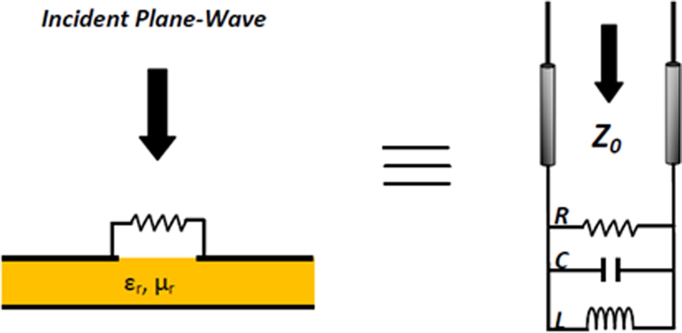
Fig. 2. Electric equivalent circuit of the R-HIS.
The expressions for the reflection coefficients ΓTE and ΓTM corresponding to the two polarizations of the incident wave (respectively TE and TM) are [Reference Tretyakov14]:
where Z sTE/TM refers to the surface impedance of the R-HIS for the TE and TM polarized incident fields and θ is the incident angle. The surface impedance Z s of the R-HIS can be considered to be a parallel connected capacitance C, an inductance L and a resistor R:
From [Reference Luukkonen15], the formulas of the capacitance and inductance for each polarization of the incident field are

where P = w + g is the period of the structure, ![]() is the normal component of the wave vector in the substrate with k the wave vector in the substrate and k t the tangential wave vector component imposed by the incident wave.
is the normal component of the wave vector in the substrate with k the wave vector in the substrate and k t the tangential wave vector component imposed by the incident wave. ![]() is the wave vector in the effective host medium, ε 0 and µ 0 are, respectively, the permittivity and permeability of free space,
is the wave vector in the effective host medium, ε 0 and µ 0 are, respectively, the permittivity and permeability of free space, ![]() is the free space impedance and
is the free space impedance and ![]() is the dyadic unit. To improve the accuracy of the expression of ε eff, the closed expression given by Schneider has been used [Reference Schneider16]:
is the dyadic unit. To improve the accuracy of the expression of ε eff, the closed expression given by Schneider has been used [Reference Schneider16]:
Following the notations above, the dimensions of the structure studied are: P = 4 mm, g = 0.4 mm, h = 1 mm, and ε r = 10.2. The value of the permittivity has been chosen to reduce the dependency on angle of the absorber. The analytical results are compared with numerical simulations obtained with CST MWS. The simulation model of the R-HIS is depicted in Fig. 3. The periodicity of the unit cell is achieved by using Floquet port and periodic boundary conditions.

Fig. 3. View of the unit cell for simulation.
III. INFLUENCE OF THE RESISTOR ON THE HIS
The equivalent circuit allows us to quickly determine the frequency resonance of the HIS. This frequency corresponds to 8.7 GHz observed in Fig. 4 when the HIS is illuminated by a normal incident plane wave. This result slightly differs from the simulation carried out with CST MWS: the difference is 300 MHz that is approximately 3.5%. Due to the all limitations of the electric model (quasi-static nature), the agreement between the results is considered reasonably good.

Fig. 4. Comparison between analytical results and CST MWS 2009: reflection coefficients versus frequency for several values of resistors: (a) phase reflection, (b) absorption, (c) real part of the surface impedance Z s, and (d) imaginary part of the surface impedance Z s.
From the expressions (1) and (2), at resonance, a HIS exhibits infinite surface impedance which occurs with the free space impedance, hence the electromagnetic incident wave is totally reflected. The surface impedance can be decreased by the use of resistors, absorbing the incoming wave when the surface impedance of the R-HIS is matched to the free space impedance 377 Ω (see Fig. 4(c)). At resonance, the expression of the reflexion coefficient can be written as
The absorption coefficient is plotted for several values of the resistors in Fig. 4(c) for a normal incident angle of the incoming wave: as expected the absorption performance is best for a value of resistance of 377 Ω. Moreover when the resistor value is increased, an abrupt change of the phase reflection is observed: at resonance, when the resistor value R is less than the free space impedance η 0, the phase of the reflection coefficient is equal to ±π. As explained above, by inserting losses in the HIS, the PMC condition cannot be reached anymore.
The reflectivity of the HIS loaded by a resistor R = 377 Ω is plotted in Fig. 5 for normal incidence and for 30 and 60° incidence angle, for both TE and TM polarizations. The analytical results agree with CST MWS with a slight at the lower frequency for the numerical simulations. The performance of the R-HIS is affected by the change of incident angle. As for the Salisbury screen the R-HIS exhibits a narrow bandwidth in frequency and in angle. As expected the resonance frequency for TE polarization of the incident wave is affected (see expression (5)).

Fig. 5. Absorption coefficient for different incident angles: (a) TE polarization and (b) TM polarization.
The equivalent electric circuit can be used to design rapidly the absorber and a simulation can be used to accurate the absorption band and the resonance of the structure.
IV. EXPERIMENTAL RESULTS
In order to validate the method, a measurement has been set up. A oversized rectangular waveguide is used to measure the absorption performance of the R-HIS. This measure uses the principle of images: the walls of the waveguide act as pairs of image planes which make the enclosed structure an infinity periodic environment. Waveguide simulators that are used to characterize antenna arrays can also be applied to periodic arrays such as FSS. Advantages and limitations of this method are described in [Reference Pearson, Phillips, Mitchell and Patel17]. The cross section of the waveguide must be commensurate to the periodicity of the structure. The dimensions of the waveguide simulator are a × b = 48 × 8 mm, where a is the large side of the waveguide. However this method has some limitations: the plane waves associated to the TE10 mode are incident at angles:
Moreover, measurements cannot be made outside the bandwidth of the TE10 mode. In the present case, the ultra-thin RAM has a 12 × 2 periodicity, and is positioned at the end of the waveguide (see Fig. 6). The 48 mm cross section of the guide, corresponds to θ = 20.05° at f = 8.4 GHz. The structure analyzed is simulated using CST MWS to be compared to measurement (see Fig. 7). In Fig. 8 the phase reflection and the absorption of a HIS and an R-HIS loaded by resistor value of 300 Ω are plotted. Without resistors mounted on the HIS, the measurement is well matched to the numerical simulation (Fig. 8(a)). Applying the same process for the R-HIS, a slight shift of 100 MHz in the upper frequency is observed with the measurement. Moreover, a 4 dB difference between the simulation and measurement is observed on the absorption (Fig. 8(b)). This magnitude difference may be due to the fabrication process: the resistor may not be accurate in high frequencies and the structure is very sensitive to the height of the substrate. However the experimental results agree with the simulations for these two studies cases, indicating the proposed analytical and numerical model are accurate to design an ultra-thin absorber.

Fig. 6. (a) The fabricated R-HIS and (b) The R-HIS placed at the end of the waveguide simulator.

Fig. 7. The rectangular waveguide simulator simulation model (a = 48 mm, b = 8 mm, D = 30 mm).

Fig. 8. Experimental and CST MWS results of the reflection coefficients of a R-HIS (R = 300 Ω) and a HIS (without R): (a) phase and (b) magnitude.
V. CONCLUSION
An ultra-thin absorber has been investigated: the total thickness of the R-HIS is λ 8.4 GHz/35. The absorption level of the RAM can be controlled by the choice of the resistor value, whereas the geometric parameters define the absorption band. The use of an electric equivalent circuit based on the transmission line approach allows a quick design of the absorber. The effects of the resistor on the R-HIS have been studied for TE and TM polarizations of the incident wave. The R-HIS performance is best when the HIS is loaded by a resistor equal to the free space impedance. The analytical results have been compared to simulations done with CST MWS. A good agreement has been observed between the results despite a slight shift in frequency: a simulation can be done to get accurate results. All these results have been validated with the use of a waveguide simulator.
 Fabrice Linot was born on April 5, 1984 in Nice, France. He received a M.Sc. degree in telecommunications and radio-frequency engineering from the University of Nice and Sophia-Antipolis (UNSA), Nice, France, in 2007. Currently, he is working toward the Ph.D. degree at Telecom ParisTech (formely École Nationale des Telecommunications) and Thales Airborne Systems in the Antennas and Radomes unit, Paris, France. His current research interests include the utilization of artificial impedance and electromagnetic band gap structures in microwave applications.
 Xavier Begaud was born on December 11, 1968 in Chateaudun, France. He received a M.S. degree in optics, optoelectronics, and microwaves, with a specialization in microwaves from Institut National Polytechnique de Grenoble (INPG) in 1992. Afterwards, he received the Ph.D. degree from the University of Rennes in 1996 and the habitation degree from Pierre and Marie Curie University (Paris 6) in 2007. He joined the TELECOM ParisTech (formerly École Nationale des Télécommunications) in 1998, where he is presently an associate professor at communications and electronics department. He works with the Radiofrequency and Microwave Group and is a member of the UMR 5141 of CNRS, the French National Scientific Research Center. He gives lectures in the fields of antennas, propagation, and microwave engineering. Professor X. Begaud presents research topics including theory, conception, modeling, and characterization of wideband, bipolarized, and 3D antennas with special emphasis on numerical methods. Currently, his research activities include design of metamaterials, channel sounding, and mutual coupling analysis in the framework of ultra-wideband and software radio.
 Christian Renard was born in Casablanca, Morocco, in 1954. He received a engineering degree in electronics from the Institut Supérieur d'Electronique de Paris (ISEP), France, in 1976. In 1977 he joined the microwave department of Dassault Electronique, France, where he has been involved in the design of arrays and phased array antennas for radar and telecommunications. He is presently technical expert for antennas and radomes in the Radar & Warfare Systems Unit of THALES Aerospace Division. He holds several patents in the fields of antennas and measurements. He is a senior member of IEEE and of SEE.


