


Introduction
A transistor is the fundamental element of complex monolithic microwave integrated active circuits and can be characterized using on-wafer measurements. There are commercial impedance standard substrates (ISSs), which allow different types of on-wafer calibrations, such as short-open-load-thru (SOLT) [Reference Fitzpatrick1], line-reflect-match (LRM) [Reference Doemer and Rumiantsev2], line-reflect-reflect-match (LRRM) [Reference Hayden3], multi-line thru-reflect-line (MTRL) [Reference Marks4], etc. Commercial calibration standard substrates have appealing advantages of relatively low cost and good durability. These ISSs are usually based on thick ceramic substrates, with a thickness ranging from 250 to 600 µm, and are designed to have coplanar waveguide (CPW) structures. These ISSs provide off-wafer calibrations, when the devices are fabricated on gallium arsenide (GaAs), gallium nitride (GaN), or indium phosphide (InP). Off-wafer measurement impairs the accuracy of calibration, as reported in [Reference Willimas and Marks5] and [Reference Williams, Corson and Sharma6]. The deviation in S-parameter (scattering parameters) measurement, due to off-wafer effects, will become more significant as the frequency rises.
In recent years, on-wafer-level calibration, i.e., the Device Under Test (DUT) and the calibration kits have identical substrates, boundaries, and parasitical influences, and have been investigated extensively. A prescription for terahertz (THz) calibration kits was introduced in [Reference Williams, Young and Urteaga7], and calibration-kit design guidelines for millimeter-wave use were described in [Reference Williams, Corson and Sharma8] and [Reference Williams, Schmuckle and Doerner9] (these demonstrate an improved performance over off-wafer calibrations). Similar to ISSs, the 625-μm thick ceramic substrate calibration kits in [Reference Williams, Schmuckle and Doerner9] and the complicated calibration kits in [Reference Williams, Corson and Sharma8] are not ideal choices for measurement of transistors fabricated on thin GaAs substrates. As the frequency rises, the substrate thickness could be reduced to 70 µm or less, to minimize parasitical resistance and inductance. Additionally, cross-talk between the probes may need to be taken into account at W-band frequencies and above [Reference Williams, Young and Urteaga7], to achieve the desired measurement accuracy and results. To the best of the authors' knowledge, on-wafer-level calibration standards based on the thin substrate and operating at the W-band have not yet been reported in open literature. TFMSL (thin film microstrip lines) [Reference Heiliger, Nagel, Roskos, Kurz, Schnierder and Heinrich10] have the appealing advantage of easing single-mode propagation and are therefore another promising type of transmission line for use at millimeter-wave and THz frequencies. Compared to the CPW type of structure, TFMSL is more difficult to access in a ground state: this may prevent its wider application in the design of active circuits.
We report on W-band on-wafer-level calibration kits, based on a grounded coplanar waveguide (GCPW) structure, and fabricated on a thin (70 µm) GaAs substrate. Thin substrates with a conductor on the back are undesirable, as they can easily excite parallel-plate modes which could degrade calibration accuracy [Reference Schmuckle, Doerner, Phung, Heinrich, Williams and Arz11, Reference Deal12]. In this work, holes were utilized to suppress the excitation of parallel-plate modes. Sixteen-term calibration standards were designed for better predictions of cross-talk at these high frequencies. A comparison between 16-term and other on-wafer and off-wafer calibration methods was performed on both passive and active devices. The new GCPW calibration substrate was also employed to realize four conventional calibration methods. Investigation into their corresponding performance, with respect to MTRL, was conducted. The paper is organized as follows: Section “design of calibration kits” introduces the design of calibration kits, and Section “definition of the 16-term calibration” describes the definition of the calibration standards. Experimental results are presented in Section “experiment”, which is followed by the conclusion in Section “conclusion”.
Design of calibration kits
The 16-term error model calibration method, as described in [Reference Butler, Rytting, Iskander, Pollard and Vanden Bossche13Reference Butler, Rytting, Iskander, Pollard and Vanden Bossche14], was utilized in this work. The 16-term calibration kits include a 400-μm-long thru line and six pairs of lumped elements: resistor–resistor, short–short, open–open, resistor–open, resistor–short, and open–short, all with 200 µm offset from the beginning of the line. To ensure the accuracy of the definition for 16-term calibration kits, the TRL calibration algorithm, as reported in [Reference Marks4, Reference Williams, Wang and Arz15], has been utilized, with a calibration reference at the probe tips.
For the 16-term or MTRL to work, three requirements need to be fulfilled: (i) the transmission line should operate in quasi-transverse electromagnetic mode; (ii) resonances need to be eliminated within the frequency band of interest; and (iii) the characteristic impedance Z 0 of the transmission line should be uniform. In this work, the GCPW type transmission line, which is effectively a CPW with a finite metal boundary [Reference Schnieder, Tischler and Heinrich16], has been adopted and the thickness of the GaAs substrate is 70 µm. Such a thick substrate with a conductor on the back can easily excite unwanted multi-modes, e.g. the parallel-plate waveguide mode and surface wave mode [Reference Godshalk17]. The ground-to-ground spacing (center conductor width w plus twice the gap g between the center conductor and the ground plane on each side) has been designed to help to maintain single mode propagation [Reference Heinrich18] and to achieve the desired Z 0. Parallel-plate waveguide modes between the topside ground plane and the conductor on the back can be suppressed by introducing holes connecting the top and bottom grounds. Parts of the calibration kits are shown in Fig. 1.
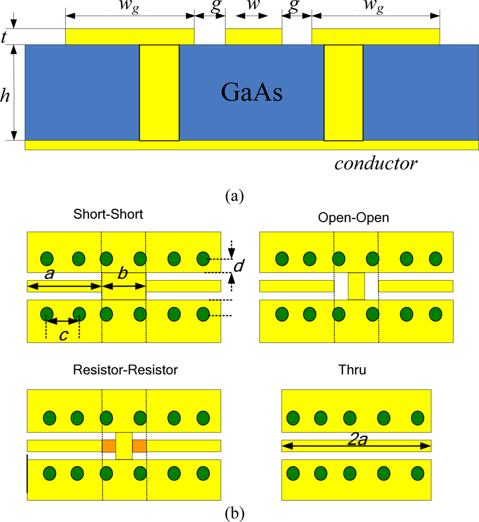
Fig. 1. Calibration standards. (a) Side view of CPW transmission line conductor on the back. (b) Short–short, open–open, resistor–resistor, and Thru elements.
The Linecalc tool in the Advanced Design System was employed to determine GCPW ground-to-ground spacing. To achieve a 50 Ω characteristic impedance, w and g were calculated to be 26 and 22 µm, respectively. These calculations utilized a substrate dielectric constant of 12.9, a substrate thickness of 70 µm, a metal conductivity of 5.7 × 10⁶ S/m and a metal thickness of 0.5 µm. Holes with a diameter of 30 µm were added between the topside ground and the rear conductor, and these holes are uniformly distributed along the GCPW line with the separation c, as shown in Fig. 1(b). The distance d, shown in Fig. 1(b), between the center of the holes to the edge of the ground plane was set to 45 µm. The optimum hole separation c was obtained from full-wave simulations in CST Microwave Studio [19]. The simulation results indicate that a separation c of 100 µm is desired, in terms of the ease of fabrication and a wide spurious free band. Therefore, c was chosen as 100 µm in this work. Note that CST simulations assumed that the holes are perfect cylinders, however in practice these holes were fabricated to have sloping side walls owing to the etching process used. The influence of this is believed to be negligible. Figure 2 shows the layout of the final calibration kits.
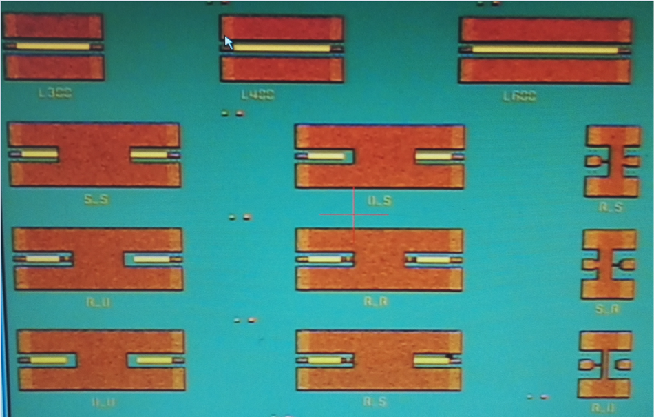
Fig. 2. Optical image showing parts of the fabricated standards.
Definition of the 16-term calibration
The MTRL calibration determines S-parameters directly in printed transmission lines and avoids many of the systemic errors associated with lumped calibrations. Here, the TRL calibration standards were fabricated with a 400-μm-long GCPW thru line (the identical Thru for 16-term), four lines with additional lengths of 100, 300, 500, and 2600 µm, and identical shorts with 16-term short–short elements. GaAs is a low-loss substrate material, and therefore it is feasible to calculate the transmission line capacitance [Reference Williams and Marks20], and to correct the reference impedance of the system to 50 Ω by following the method outlined in [Reference Marks and Williams21]. The transmission line was found, by measurement, to have a smooth attenuation constant and a flat effective permittivity (Fig. 3). This indicates that the transmission line operates mostly in single-mode propagation with little dispersion. Finally, 16-term calibration kits are defined by the MTRL corrected vector network analyzer (VNA) mentioned below, including a thru-line and the reflection coefficient of six pairs of lumped elements.

Fig. 3. Propagation constant and effective permittivity real part of the transmission line. (a) Attenuation constant and (b) effective permittivity (real part).
Experiment
The experimental set-up comprised: a Keysight N5245A, a Cascade 12 000 probe station, two OML W-band V10VNA2 extension modules, and two Cascade Infinity i110-T-GSG-100-BT probes. The pitch size of these probes is 100 µm. The DUTs are resistor–resistor and active high-electron-mobility-transistor (HEMT), both of which were fabricated on the same 70-μm-thick GaAs substrate with a conductor on the back. A single measurement of the raw (i.e., uncorrected) measurement data was acquired for each of these DUTs: a different calibration was then applied to the raw measurement data to obtain the corrected measurement data.
Measurement results: resistor–resistor
The GCPW calibration substrate includes two sets of resistor–resistor configurations with the same design. One of these was used as a standard for the 16-term calibration. Measurement was conducted on the other device, subject to two different types of calibrations, i.e., LRRM using ISS 104-783A and 16-term using the calibration kit developed here. In this work, Wincal XE 4.6 [22] was adopted to define and manage different calibrations. Figure 4 shows S 21 responses (i.e., isolation) of the resistor–resistor. It can be observed that the 16-term calibration improves the isolation by around 10 to 15 dB, compared with the LRRM technique. This demonstrates that 16-term calibration kits are capable of factoring in the effects of cross-talk.

Fig. 4. Comparison of S 21 responses between two calibration kits for resistor–resistor, as shown in Fig. 1(b).
Measurement results: high electron mobility transistor
The pHEMT transistor with a gate width of 25 µm × 4 was measured without correction. Four different types of calibrations were then applied to the raw data, to get the corrected results. These four calibrations are: LRRM using ISS placed on metal, LRRM using ISS placed on the absorbing material, 16-term using the fabricated kit placed on metal, and MTRL using the fabricated kit placed on metal. Figure 5 illustrates the results of the transistor subject to these four calibrations. It can be observed from Fig. 5 that the testing environment affects the ISS, with the absorbing material yielding the better result. There is good agreement between the results from MTRL and 16-term calibrations. This indicates that cross-talk is not a dominant factor in the measurement of transistors. Note that other transistors fabricated on the same batch were also found to produce similar results.
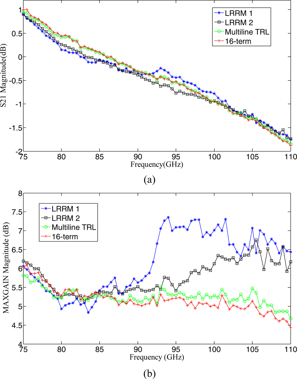
Fig. 5. Measurement results: (a) S 21 magnitude and (b) Maxgain, associated with four calibration techniques. LRRM 1 corresponds to ISS on metal, LRRM 2 represents ISS on the absorbing material, MTRL and 16-term configurations were tested by using a GCPW calibration substrate placed on metal.
Comparison of different calibrations using standards on GCPW substrate
The fabricated GCPW calibration substrate was also used to implement different calibrations, i.e., SOLT, LRM, LRRM, and MTRL. A calibration comparison [Reference Willimas and Marks5] was carried out to qualify the differences between these calibrations with respect to the MTRL (a well-known, and precise, technique). Figure 6 shows the maximum difference between the results obtained from MTRL and the other three techniques. LRRM returns the worst difference of 0.17, this may be attributed to LRRM's assumption of an intrinsic shunt-load [Reference Liu, Ocket, Lewandowski, Schreurs and Nauwelaers23]. SOLT and LRM demonstrate a promising result and exhibit a difference of less than 0.1 across the whole W-band. The small difference between the two MTRL results demonstrates the good measurement repeatability. As shown in Fig. 6, the difference between a MTRL and an LRM or LRRM calibration using standards pre-characterized with MTRL is higher than the system drift (i.e., MTRL2–MTRL1). It is believed that this is attributed to errors in fabrication, resulting in a characteristic impedance of the transmission line of 48.6 Ω and a match resistance of 51.8 Ω, instead of the designed nominal value of 50 Ω. This deviation can be addressed when the process becomes more developed.

Fig. 6. Calibration comparison results between MTRL and SOLT (star), LRM (square), LRRM (circle), and another MTRL (plus).
Conclusion
Thin GaAs calibration kits based on GCPW structures have been presented. This new type of calibration kit enables accurate on-wafer-level measurements, at W-band frequencies and beyond. Sixteen-term calibration was conducted and was compared with off-wafer LRRM and on-wafer MTRL calibrations. The comparison, on both passive and active devices, demonstrates that 16-term is capable of better determining isolation: however, the difference between 16-term and MTRL is insignificant, and therefore the latter might be sufficient when cross-talk or isolation is not critical. Different calibration techniques were investigated using standards set by the new calibration kits. Generally, SOLT and LRM offered better results over LRRM, assuming MTRL gives an accurate and reliable result. This investigation was carried out at W-band frequencies, and all measurements were the on-wafer-level (i.e., the DUT and the calibration standards were fabricated on the same substrate). Overall, the work presented in this paper demonstrates the promising potential for the utilization of thin GaAs calibration kits, with GCPW structures, for high-frequency on-wafer-level probing.
Acknowledgement
The authors thank Southeast University, China, for providing the W-band on-wafer S-parameter measurement system used in the research described herein.
 Yibang Wang was born in Jining, Shandong, China, in 1987. He received a BS in Communication Engineering from Nanjing University of Aeronautics and Astronautics, and an MS in Instrument Design from the Handan Purified Equipment Research Institute in Hebei, China, in 2012. Then he joined the microwave calibration and test division, Hebei Semiconductor Research Institute in Shijiazhuang, China. His current research interests include: microwave metrology, particularly on-wafer terahertz S-parameter measurements, the fabrication of on-wafer calibration kits, and the development of calibration algorithms.
 Xingchang Fu was born in Laiwu, Shandong, China, in 1975. He received a BE in Microelectronic Technology from Hunan University, Changsha, China, in 1999. He is currently pursuing a PhD degree in Southeast University, Nanjing, Jiangsu, China. He joined the Hebei Semiconductor Research Institute, Shijiazhuang, in 1999, where he is currently a Professor with the Microwave & Millimetre Wave Chip Process Department. His current research interests include microwave semiconductor processes and on-wafer measurement.
 Aihua Wu was born in Zhangjiakou, China, in 1980. He received BS and ME degrees in Microelectronics from Jilin University, Changchun, China, in 2004 and 2007, respectively. He joined the Hebei Semiconductor Research Institute, Shijiazhuang, in 2007, where he is currently a Senior Research Engineer with the Metrology Centre. In 2017, he joined the National Physical Laboratory, Teddington, UK, as a Visiting Researcher. His current research interests include: microwave metrology, particularly on-wafer noise measurements and instrumentation, and the fabrication of on-wafer devices for ultra-wideband S-parameters and noise parameter calibration and verification.
 Chen Liu was born in Hengshui, Hebei, China, in 1986. He received BE and ME degrees in Measuring and Testing Technologies and Instrumentation from Xidian University, Xi'an, China, in 2009 and 2012, respectively. He joined the Metrology Centre, Hebei Semiconductor Research Institute, Shijiazhuang, China, as a Research Engineer in 2012. In 2017, he joined the National Physical Laboratory, Teddington, UK, as a Visiting Researcher. His current research interests include: the design and characterization of on-wafer SOLT and TRL S-parameter calibration kits, the development of accurate on-wafer S-parameter and noise parameter measurement techniques, and the verification of on-wafer S-parameters and noise parameters using active and passive devices.
 Peng Luan was born in Liaoning, China, in 1978. He received a BEng from North Eastern University, Shenyang, China, in 2002, and an MSc from University of Electronic Science and Technology of China, Chengdu, China, in 2011. He joined the Metrology Centre, Hebei Semiconductor Research Institute, Shijiazhuang, China, as a Research Engineer in 2002. His current research interests include the design and characterization of on-wafer TRL S-parameter calibration kits, the development of accurate on-wafer S-parameters and load-pull system measurement techniques, and the verification of on-wafer S-parameters and load-pull systems using active and passive devices.
 Faguo Liang was born in Liaocheng City, Shangdong Province, China, in 1965. He received a BE in Microelectronics from Shangdong University in 1984, and an ME in Microelectronics from Hebei Semiconductor Research Institute in 1989. From 1984 to 1986, he was a Research Assistant with the Jinan Semiconductor Research Institute, China. Since 1989, he has been an Engineer with the Hebei Semiconductor Research Institute, China. Now, he is a Professor and his current research interests include microwave instrumentation metrology and on-wafer microwave parameter measurements.
 Wei Zhao received his PhD in Communication and Information Systems from Nanjing University of Aeronautics and Astronautics, Nanjing, China, in 2011. He joined the School of Electro-Mechanical Engineering, Xidian University, Xi'an, in 2011. From 2014 to 2015, he was a Guest Researcher with the National Institute of Standards and Technology, Boulder, Co., USA. His current research interests include VNA calibration and uncertainty analysis.
 Xiaobang Shang received a BEng (First Class honors) in Electronic and Communication Engineering from The University of Birmingham, UK, in 2008, alongside a BEng in Electronics and Information Engineering from Huazhong University of Science and Technology (HUST), China, in 2008, and a PhD in Microwave Engineering from The University of Birmingham, UK, in 2011. He is currently a Senior Research Scientist at the National Physical Laboratory (NPL), UK: before joining the NPL, he was a Research Fellow with The University of Birmingham. His current research interests include microwave measurements and microwave circuits. Dr. Shang was the recipient of the ARFTG Microwave Measurement Student Fellowship Award in 2009, the co-recipient of the Tatsuo Itoh Award in 2017, and the recipient of the Steve Evans-Pughe prize (awarded by ARMMS RF and Microwave Society) in 2017.


