I. INTRODUCTION
Mixers play an important role in wireless communication systems. System requirements entail many considerations, such as conversion gain, noise figure (NF), port-to-port isolation, and linearity [Reference Maas1–Reference Lee3]. Moreover, both dc power consumption and local oscillator (LO) drive power should be low in a low-power millimeter-wave (MMW) communication system.
Although passive mixers have good linearity, the high LO drive power poses a challenge to integration in a CMOS MMW transceiver [Reference Kuo, Kuo, Kuo, Maas and Wang4–Reference Chen, Kuo, Hsin and Wang7]. On the other hand, the resistive and drain mixers usually have large LO-RF feedthrough [Reference Ellinger8]. Among the active mixers, the Gilbert-cell mixer has rather high dc power and requires high voltage [Reference Tseng, Meng, Chang, Chang and Huang9]. Unlike other active mixers, gate mixers have more efficient conversion gain at low LO drive power, low power consumption, and low supply voltage; however, the LO-RF feedthrough is also a severe impediment [Reference Ellinger8]. To enhance the RF port to LO port isolation, a rat-race hybrid, which provides in-phase and out-of-phase signals at the same time in a balanced mixer, is utilized in a balanced gate-pumped mixer. However, the conventional rat-race hybrid, especially the one that operates at lower frequencies, occupies a large chip area [Reference Tseng, Meng, Chang, Chang and Huang9]. Although a miniature 60 GHz rat-race hybrid has been proposed in [Reference Lien, Wang, Lin, Wu, Lin and Wang10, Reference Lien, Wu, Lin and Wang11], the rat-race hybrid is still large when it is applied in lower frequency applications, for example, below 30 GHz. The design procedure of the rat-race hybrid in [Reference Lien, Wang, Lin, Wu, Lin and Wang10, Reference Lien, Wu, Lin and Wang11] is also complex. A combined hybrid is proposed in [Reference Lien, Huang, Kao, Lin and Wang12], but that double-balanced architecture still occupies a large area and has high dc power consumption. Moreover, the design considerations and procedures of a single-balanced gate-pumped mixer have not been described in detail in the literature.
In this paper, a miniature rat-race hybrid is proposed and analyzed. This rat-race hybrid occupies a smaller area than those in [Reference Lien, Wang, Lin, Wu, Lin and Wang10–Reference Lien, Huang, Kao, Lin and Wang12] at the same operation frequency. In addition, a rat-race single-balanced gate-pumped mixer is developed with very low LO power (−4.3 dBm). The design considerations and simplified design procedures of the single-balanced gate-pumped mixer with a rat-race hybrid are also described in detail.
II. CIRCUIT ARCHITECTURE
The presented rat-race single-balanced gate-pumped mixer is shown in Fig. 1. It is composed of a proposed miniature rat-race hybrid, gate-pumped mixers, and source followers.
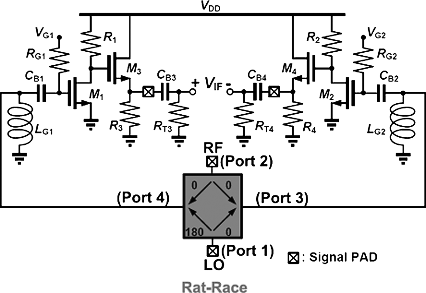
Fig. 1. A single-balanced gate-pumped mixer.
The gate pumped mixers consist of transistors M 1 and M 2, load resistors R 1 and R 2, gate-biased resistors R G1 and R G2, blocking capacitors C B1 and C B2, and input-matching inductors L G1 and L G2.
To drive low impedance loads (R T3 and R T4) the source follower output buffers for signal amplification and impedance transformation are used. Source followers, which comprise transistors M 3 and M 4 and load resistors R 3 and R 4, provide suitable gain for the mixer.
The schematic of the proposed miniature rat-race hybrid in Fig. 1 is shown in Fig. 2(a). The miniature rat-race hybrid can be implemented with a Marchand balun and thin-film microstrip (TFMS) lines to achieve the out-of-phase and in-phase signals at the output port [Reference Lien, Wang, Lin, Wu, Lin and Wang10, Reference Lien, Wu, Lin and Wang11]. The Marchand balun can achieve a low loss with the ground plane shielding the high substrate loss. However, in this paper, the TFMS is replaced with a symmetric inductor L s to achieve in-phase signals at the output port, as shown in Fig. 2. As can be observed, there is no ground plane under the symmetric inductor, so the routing length can be shorter than the TFMS line while still achieving the same inductance, thus reducing the size of the inductor, as well as its loss. Fig. 2(b) shows the layout of the proposed miniature rat-race hybrid, which is smaller than 150 µm × 200 µm.

Fig. 2. (a) Schematic and (b) layout of the proposed miniature rat-race hybrid.
III. CIRCUIT DESIGN
A) Device size and bias condition selection
The device f T of nMOS reaches around 110 GHz in 90 nm CMOS [Reference Razavi13]. Although 90 nm digital CMOS technology does provide a top thick metal layer, the 9-layer interconnecting metals can provide a high density fringe capacitor [Reference Lee, Liu and Wang14].
The V gs is usually biased near the threshold voltage V TH, 0.2 V, and the channel width is 250 µm, respectively.
B) Rat-race hybrid
In order to achieve a higher LO-to-RF isolation in a mixer, the symmetry of the rat-race hybrid is important. For example, the output signals of port 3 and port 4 (Fig. 2) in the rat-race are
and
where ΔV RF, θ, and ϕ are the amplitude and phase offset of the RF path (in-phase), and LO path (out-of-phase), respectively. The effects of phase and amplitude mismatch for the RF-to-LO isolations in a gate mixer are shown in Figs 3 and 4. The simulation results are obtained by using 90 nm CMOS models provided by the foundry with an ideal 180° balun with variable phase and amplitude offsets. As can be observed, the in-phase signal is more sensitive than the out-of-phase signal. Fortunately, it is easy to lower the phase and amplitude mismatch to below 1° and 0.25 dB, respectively, by using a symmetric inductor, thus leading to an RF-to-LO isolation of a mixer higher than 40 dB.

Fig. 3. RF-to-LO isolations of the mixer versus phase offset.

Fig. 4. RF-to-LO isolations of the mixer when ΔV RF and ΔV LO are varied.
In order to minimize chip area, we use the reduced-size Marchand balun. However, the design of the reduced-size Marchand balun is quite complex because of the multiple design parameters in a distributed structure [Reference Lien, Wang, Lin, Wu, Lin and Wang10, Reference Lien, Wu, Lin and Wang11]. Fortunately, if we use a lumped-element model, these design parameters are closely related to only one key parameter, namely the total routing length (ℓ), which greatly simplifies the design of the balun and is defined in this paper. In the preliminary design of the balun, the design procedures are described as follows:
(1) Select a lumped-element model for TFMS lines, as shown in Fig. 5(a).
(2) Determine the relationships between L 1, C 2, R 1, and routing length (ℓ) through electromagnetic (EM) simulation based on a 3 µm wide and 100 µm long TFMS line, as shown in Fig. 5(b). The choice of the 3 µm width is determined by the design rule and consideration of loss. In our case:
(1) (2)(3)
(3) Determine the relationships between C 1 and routing length (ℓ) through EM simulation based on a pair of edge-coupled lines with a width of 3 µm, spacing of 3 µm, and length of 100 µm, as shown in Fig. 5(c). Again the spacing of 3 µm is determined by the process design rule and reasonable coupling.
(4)(4) Select the lumped-element model of the balun with the lumped-element model of TFMS lines, as shown in Fig. 5(d). Note that the output ports are port 3 and port 4, and the input port is port 1. Therefore, the amplitude mismatch is defined as the amplitude difference at port 3 and port 4, while port 1 is an input signal. On the other hand, the phase mismatch is defined as the phase difference at port 3 and port 4, while port 1 is an input signal.
(5) Determine the relationships between C M and routing length (ℓ) through EM simulation based on a pair of broadside-coupled lines with a signal line width of 3 µm, spacing of 0.715 µm, and length of 100 µm, as shown in Fig. 5(e).
(5)(6) Determine the total routing length based on the simulated frequency responses of phase and magnitude differences at the output ports. Referring to [Reference Lien, Wang, Lin, Wu, Lin and Wang10], the total routing length is around 300 µm (ℓ) at 24 GHz. Figure 6 presents the simulated mismatch and phase difference of this balun from 20 to 30 GHz when the routing length is 310 µm. It can be observed that this routing length (310 µm) makes this balun operate at 24 GHz (amplitude mismatch = 1.5 dB; phase difference = 180°).

Fig. 5. (a) Lumped-element model of TFMS lines, (b) a 3 µm wide and ℓ µm long TFMS line, (c) a pair of edge-coupled lines with a width of 3 µm, spacing of 3 µm, and length of ℓ µm, (d) lumped-element model of the simulated Marchand balun, and (e) a pair of broadside-coupled lines with a width of 3 µm, spacing of 0.715 µm, and length of ℓ µm.
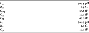
The selected parameters of this model, as shown in Table 1, are obtained through curve fitting via the Advanced Design System (ADS) and the Sonnet simulation tool. Due to the lumped-element model, the simulated frequency responses in Fig. 6 are not quite wideband. However, this simulated result still can provide insight for preliminary implementation of the physical layout of the reduced size Marchand balun. The routed length of the balun is preliminarily determined based on the value of L sp in Table 1, and the final balun is determined through EM simulations for the precise size of the balun. In addition, the frequency responses of the EM simulations are wideband, unlike those of the lumped-element model of TFMS lines. In order to reduce the size, the width and space of the routing of this balun are 3 µm. Furthermore, the outer radius and turn number of each spiral line are 55 µm and 5, respectively. With these selections, the Marchand balun has phase and amplitude mismatches of less than 2° and 0.5 dB at 24 GHz, respectively (Fig. 7). With such properties, the RF-to-LO isolation of the mixer is better than 30 dB (Figs 3 and 4).

Fig. 6. Amplitude mismatch and phase difference of the simulated lumped-element model for the Marchand balun (ℓ = 310 µm) from 20 to 30 GHz.

Fig. 7. Amplitude mismatch and phase difference of the EM-simulated Marchand balun from 20 to 30 GHz.
Table 1. Design parameters of the model for reduced size Marchand balun (ℓ = 310 µm).

IV. EXPERIMENTAL RESULTS
A test circuit of the rat-race hybrid has also been fabricated, as shown in Fig. 8. The corresponding EM-simulated and measured insertion losses are shown in Fig. 9. As can be seen, the insertion loss from port 2 to port 3 (or port 4) is lower than 7.5 dB when the operation frequencies are higher than 15 GHz, and the simulation and measurement results agree well. In mixer application, the power level of the RF signal is very low; thus, port 2 is assigned to be the RF port in this design to maintain the required conversion gain. Owing to the 0.85 µm thickness of the top-metal in the digital process, the insertion loss is a little bit high, but we can slightly reduce the loss by reducing the length of the routing as much as possible. This proposed low-power miniature single-balanced gate mixer has been fabricated in 90 nm digital CMOS technology, as shown in Fig. 10.

Fig. 8. Die photo of the rat-race hybrid.

Fig. 9. EM-simulated and measured insertion loss of the rat-race hybrid.

Fig. 10. Die photo of the single-balanced gate-pumped mixer.
The die photo of the mixer is shown in Fig. 10. The chip area is 0.49 mm × 0.49 mm, including the testing pads. The core area is very small, occupying only 0.26 mm × 0.2 mm. It consumes 6 mW including buffers from a 1.2 V supply. Figure 11 shows the measured conversion gain of the mixer from RF frequencies of 10–40 GHz with a total supply current of 5 mA. The simulated conversion gain agrees reasonably with the measured one. The RF-to-LO isolation of the gate mixer is shown in Fig. 12. The isolation is better than 30 dB from 17 to 40 GHz. The measured RF return loss is shown in Fig. 13, and the return loss is very wideband as well. Table 2 presents a performance summary of the mixer alongside other reported mixers at similar operation frequencies. The developed mixer achieves a conversion gain of −1 dB with a very low LO power level of −4.3 dBm and a high LO-to-RF isolation of the gate mixer up to 30 dB at the same time. Due to the loss of the symmetric inductor, the NF is a little bit higher. But the proposed miniature rat-race hybrid is smaller than all those previously reported.

Fig. 11. Conversion gain versus RF frequency (IF frequency = 0.1 GHz).

Fig. 12. RF-to-LO isolation of the gate mixer versus RF frequency.

Fig. 13. RF return loss of the gate mixer.
Table 2. Performance summary and comparisons.

V. CONCLUSION
This paper presents a miniature rat-race hybrid for a gate-pumped mixer that achieves lower conversion loss and higher port-to-port isolation. In addition, the design considerations and procedure are described in detail. The experimental results are presented to verify the proposed miniature hybrid rat-race and the design considerations and procedure for a gate-pumped mixer. From the experimental results, it is concluded that our proposed mixer can indeed achieve a low conversion loss and a high port-to-port isolation with a low LO power and lower dc power consumption at the same time. Finally, the demonstrated miniature single-balanced gate-pumped mixer appears to be suitable for integration in a low-power receiver with a small size.
ACKNOWLEDGEMENT
This work was supported in part by the NTU-TSMC Joint Development Program, National Science Council of Taiwan (NSC 97-2219-E-002-015 and NSC 96-2220-E-002-001), and Excellent Research Projects of NTU (97R0062-03 and 97R0533-1). The authors thank the Chip Implementation Center (CIC), Taiwan, for supplying the EDA tools used in the chip design and for assistance in chip measurements.
 Chung-Chun Chen (S'03–M'09) received the B.Sc. degree from National Chiao Tung University, Hsinchu, Taiwan, in 2002, and the M.S. and Ph.D. degrees from National Taiwan University (NTU), Taipei, Taiwan, in 2004 and 2009 respectively, all in electrical engineering. After one year of military service (2009–2010), he was with Taiwan Semiconductor Manufacturing Company (TSMC), Hsinchu, Taiwan in 2010, and subsequently in Samsung Electro-mechanics America in 2011. After that, he joined Silicon Creations, Atlanta, GA, where he is currently a senior circuit designer. His current research interests include high-speed wireline transceiver for USB2/USB3, HDMI, and systems.
 Chun-Hsien Lien was born in Taipei, Taiwan, in 1976. He received the B.S. degree in communication engineering from National Chiao Tung University, Hsinchu, Taiwan, in 1998, and the Ph.D. degree in communication engineering from National Taiwan University, Taipei, Taiwan, in 2009. From January 2009 to July 2009, he was a Post-Doctoral Research Fellow with the Graduate Institute of Communication Engineering, National Taiwan University. From July 2009 to October 2010, he was a Senior Engineer with Universal Scientific Industrial Co., Nan-Tou, Taiwan. He is currently a Technical Applications Manager at Advanced Communication Engineering Solution Co. Ltd. His research interests include the design and analysis of RF, microwave and MMW circuits, Signal Integrity, EMI, and computational electromagnetic.
 Hen-Wai Tsao (M'90) was born in Taipei, Taiwan, Republic of China, in 1953. He received the B.S., the M.S., and the Ph.D degrees in electrical engineering from National Taiwan University in 1975, 1978, and 1990, respectively. Since 1978, he has been with the Department of Electrical Engineering, National Taiwan University, Taipei, Taiwan, Republic of China, where he is currently a professor. His main research interests are broadband communication system, communication electronics, and related electronic circuits.
 Huei Wang (S'83–M'87–SM'95–F'06) was born in Tainan, Taiwan, on March 9, 1958. He received the B.S. degree in electrical engineering from National Taiwan University, Taipei, Taiwan, in 1980, and the M.S. and Ph.D. degrees in electrical engineering from Michigan State University, East Lansing, Michigan in 1984 and 1987, respectively. During his graduate study, he was engaged in the research on theoretical and numerical analysis of electromagnetic radiation and scattering problems. He was also involved in the development of microwave remote detecting/sensing systems. In 1987, Dr Wang joined Electronic Systems and Technology Division of TRW Inc. He has been an MTS and Staff Engineer responsible for MMIC modeling of CAD tools, MMIC testing evaluation and design, and became the Senior Section Manager of MMW Sensor Product Section in RF Product Center. He visited the Institute of Electronics, National Chiao-Tung University, Hsin-Chu, Taiwan, in 1993 to teach MMIC-related topics and returned to TRW in 1994. He joined the faculty of the Department of Electrical Engineering of National Taiwan University, Taipei, Taiwan, Republic of China, as a Professor in February 1998. He served as the Director of Graduate Institute of Communication Engineering of National Taiwan University from August 2006 to July 2009. Dr Wang is a member of the honor society Phi Kappa Phi and Tau Beta Pi. He received the Distinguished Research Award of National Science Council, Taiwan, in 2003. He was the Richard M. Hong Endowed Chair Professor of National Taiwan University in 2005–2007. He was elected as an IEEE Fellow in 2006, and has been appointed as an IEEE Distinguished Microwave Lecturer for the term of 2007–2009. Dr Wang received the Academic Achievement Award from Ministry of Education, Taiwan, in 2007, and the Distinguished Research Award from Pan Wen-Yuan's Foundation in 2008. He is currently a National Chair Professor of Ministry of Education, Taiwan, Republic of China, for the term from February 2011 to January 2014.