


I. INTRODUCTION
The past decade has witnessed significant advances for low emittance upgrades of existing storage sources and new synchrotron facilities (Hettel, Reference Hettel2014). Together with these developments, X-ray optics have played a crucial enabling role in preserving the beam quality in manipulating and delivering X-ray photons tailored to a variety of experimental requirements (Cocco et al., Reference Cocco, Idir, Morton, Raimondi and Zangrando2018). Given that the interaction of X-rays with matter is weak, X-ray optics are usually fabricated and implemented with special configurations when compared to their visible light analogs to achieve the same (or similar) function (Ice et al., Reference Ice, Budai and Pang2011). The X-ray transmission mirror (XTM), a novel class of high-pass X-ray filters, is an example of such an optic. High-pass filtering for X-rays is traditionally accomplished with the use of absorption filters. These are thin-film metal foils inserted in the path of the beam to absorb the lower-energy photons of the X-ray spectrum as illustrated in Figure 1(a). The absorption relationship is described by the Beer–Lambert–Bouguer law,  $I\lpar E \rpar = I_0\lpar E \rpar {\rm exp}\lpar {-\mu \lpar E \rpar x} \rpar \comma \;$ and it illustrates how the energy-dependent linear attenuation μ(E) reduces the intensity of an X-ray beam I 0(E) traversing the foil with thickness x to a measured value of I(E). From this relation, the energy cutoff for a high-pass filter can be determined by the combination of the element of choice for the foil and its thickness. These criteria are usually based on an acceptable level of the low-energy photon suppression below the defined energy cutoff in comparison to the desired high-energy photons passed. Given that the absorption process is governed by an exponential relationship, this cutoff criteria is not sharp.
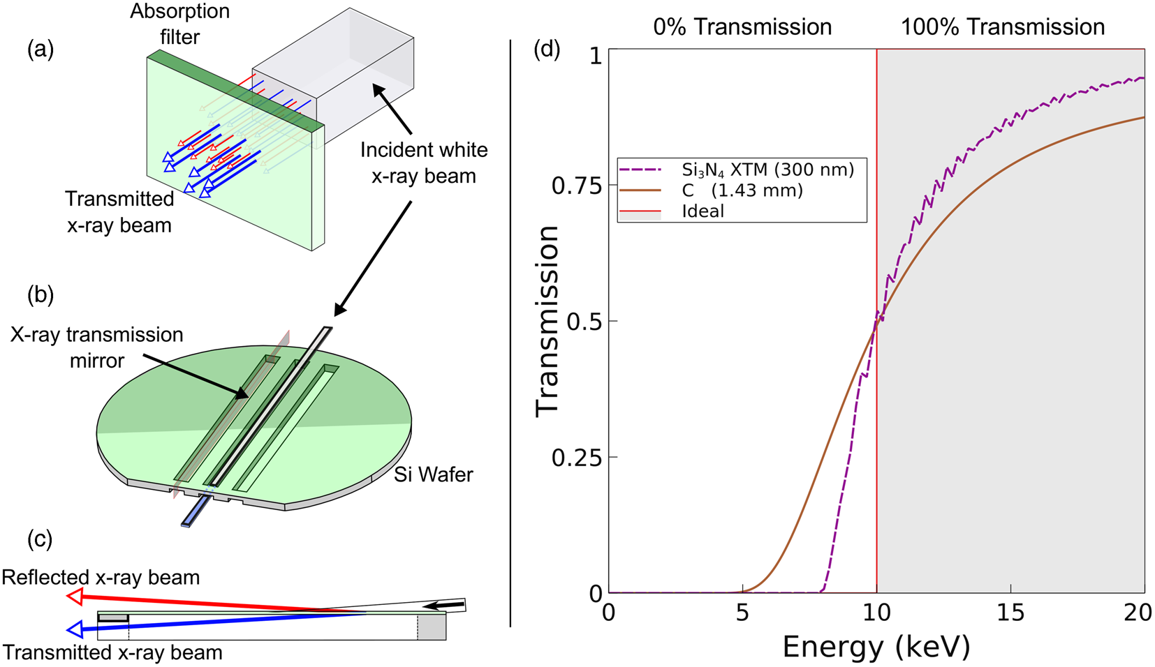
Figure 1. (Color online) High-pass filtering of a white X-ray beam. (a) Using an absorption filter. (b) Using an XTM optic. (c) Cross section through the left XTM window in (b) illustrating the specular reflection and transmission of X-rays. The solid gray box at the exit represents the structural membrane support. The cross-hatched box represents the etched clearance for the transmitted beam to leave the optic unblocked. (d) Calculated transmission response of an ideal high-pass filter, an absorption filter, and a silicon nitride transmission mirror for 50% transmission (Henke et al., Reference Henke, Gullikson and Davis1993). Red: low-energy photons and Blue: high-energy photons.
XTM optics as an alternative to absorption filters have a tunable and sharper energy cutoff. The operating mechanism is possible because the optics are designed to combine the principle of total external reflection (TER) of X-rays at grazing incidence and transmission through a thin membrane. Conceptually, the schematic in Figures 1(b) and 1(c) illustrates the working principle. The optic relies on the high efficiency of X-ray mirrors to reflect off low-energy photons below a critical energy. Given that the reflecting membrane is sufficiently thin, the complementary high-energy photons in the beam usually absorbed in the underlying substrate of the mirror is transmitted and in the process, create an efficient high-pass X-ray filter. Filtering with XTM optics, therefore, depends on the material of the reflective mirror surface and its corresponding thickness (for transmission). In addition, the incident angle of the mirror in operation is adjustable to tune the energy cutoff. Figure 1(d) compares the calculated transmission response (Henke et al., Reference Henke, Gullikson and Davis1993) at 10 keV for 50% transmission using an ideal filter, a carbon filter (1.43 mm thick), and a silicon nitride XTM (300 nm thick). In practice, for a carbon filter, the foot of the transmission response curve extends out to about 5 keV, whereas for the XTM, this is about 7 keV, illustrating the difference in the transmission response of the two filters.
The concept and original prototype XTM optic was developed and demonstrated at the Cornell High Energy Synchrotron Source (CHESS) (Lairson and Bilderback, Reference Lairson and Bilderback1982) using soap bubble films stretched on a 25-μm diameter wire in an 8 cm × 20 cm frame. The films though stable were fragile and lasted a few hours in the synchrotron beam in a wet helium environment. To improve upon the durability and make its implementation practical, subsequent developmental efforts utilized stretched Mylar films (Iida et al., Reference Iida, Matsushita and Gohshi1985) and most recently, silicon nitride thin films on silicon wafers (Cornaby and Bilderback, Reference Cornaby and Bilderback2008).
XTM optic development so far has yielded conspicuously few implementations in the literature (Cornaby et al., Reference Cornaby, Szebenyi, Smilgies, Schuller, Gillilan, Hao and Bilderback2009). This absence is largely due to the unsolved challenge of XTM fabrication: namely that the comparatively thick frame that mechanically supports the thin, reflecting membrane does not itself block the transmitted beam, given that the optic operates at grazing incidence angles. All attempts so far have not been able to address the issues to make XTMs fully functional and practical – i.e., a robust support frame and an inorganic membrane. A previous attempt by our research group (Agyeman-Budu, Reference Agyeman-Budu2019) implemented an approach which implemented a spin-cast SU-8 thin film on a silicon wafer frame. Even though successful, an organic thin film will have a limited lifetime due to the residual dose absorbed by the SU-8 polymer. The challenge, therefore, is implementing the XTM optics fabricated from low-stress silicon nitride (Si3Nx), which is a radiation hard material and can last in an X-ray beam together with a robust frame.
II. SILICON NITRIDE XTMs
Certain key criteria must be addressed to achieve the long-standing goal of fabricating both functional and practical XTM optics. For functionality, the XTM needs to have an appropriate length to accommodate the long footprint of the X-ray beam at grazing incidence. Therefore, it is essential that the mirror membrane is sufficiently thin to minimize absorption of the transmitted beam. The reflecting surface also needs to be appropriately figured and flat (Lairson and Bilderback, Reference Lairson and Bilderback1982). For practicality, the thin reflecting membrane must be anchored on all sides onto a structurally robust frame. Such a frame should also not occlude the path of the transmitted beam at grazing exiting angles when in operation. Thus, a practical working XTM prototype would be a freestanding thin-film membrane that is anchored and supported on all sides on a frame with the exit thinned down to create a support bridge with adequate clearance for the transmitted beam to exit the optic.
A. The windowing material
The choice of material depends on the (electron) density of the reflecting surface, which in turn is directly proportional to the critical angle (α c) for TER as expressed in the following equation:
 $$\alpha _c = \sqrt {2\delta } = k\sqrt \rho \lambda $$
with k being a constant defined as follows:
 $$k = \left[{\displaystyle{1 \over \pi }\;\left({\displaystyle{{e^2} \over {mc^{2\;}}}} \right)N_0\displaystyle{{\lpar {Z + \Delta {\,f}^{\prime}} \rpar } \over A}} \right]^{1/3}$$
where ρ is the density, N 0 is Avogadro's number, A is the atomic weight, Z is the atomic number with the term (Z + Δf ′) being the real part of the scattering factor for the mirror, and the constant k (k is almost a constant, depending weakly on λ. Although Δf ′ changes with λ, generally Z ≫ Δf ′) is given as 1.64 × 10⁻³ (Bilderback, Reference Bilderback1982). For instance, the critical angle for TER for a 10 keV incident monochromatic X-ray beam with dimensions of 0.5 mm × 0.5 mm (V × H) on a silicon nitride membrane (ρ = 3.44 g cm−3) can be calculated to be  $\alpha _{\rm c} = 1.64 \times 10^{{-}3}\sqrt {3.44} \lpar {12.398/{E\;}\lsqb {{\rm keV}} \rsqb } \rpar \approx 3.77\;{\rm mrad}$. Considering the geometric considerations illustrated in Figure 1(c), the incident beam will have an estimated footprint expressed as follows:
 $$l_{{\rm foot}} = \displaystyle{H \over {\sin \alpha _{\rm c}}}$$
which gives the value for l foot as 133 mm. This implies that silicon wafer substrates larger than 100 mm diameter are required to fabricate practical XTM optics. Figure 2 shows a plot that summarizes how the different material choices relate to the critical energy cutoff and the corresponding critical angles, and how that links to l foot for the case of 10 and 17 keV monochromatic X-rays. As plotted, denser materials have higher critical angles and the beam footprints are correspondingly smaller, which in general is a favorable trend. However, denser materials need to be extremely thin, which might be limited by the need to have the film thicker than penetration depth of the evanescent wave (λ/2πα c). Also, from a microfabrication perspective, such a freestanding membrane may be impractical to fabricate.

Figure 2. (Color online) Calculated plots of how the beam footprint (blue diamonds) and critical angles (dark red circles) vary with density for various materials at critical energies of 10 keV (solid line) and 17 keV (dashed line). The height of the incident X-ray beam on the XTM is assumed to 0.5 mm tall.
B. The membrane support
The membrane support is created as an etched-out window in a silicon wafer as illustrated in Figure 1(b). In our CAD design, this is accomplished by defining rectangular windows. An additional line grating pattern is inserted at the exit (downstream) of the window pattern as illustrated in Figure 3(h). Due to aspect ratio dependent etching (ARDE) effects (Jansen et al., Reference Jansen, Boer, Unnikrishnan, Louwerse and Elwenspoek2009), the close-packed grating pattern at the exit will etch slower in comparison to the open window. After processing, the resulting cross-sectional profile in Figure 1(c) shows that the window frame at the exit is partially etched out to allow the beam to exit the optic. The design and processing improvements in our microfabrication approach combines standard photolithography [see Figures 3(a)–3(c)] with a two-step etch process involving deep reactive ion etching (DRIE) and a clearing etch step [Figures 3(d)–3(g)]. The flexibility of this microfabrication approach decouples the processing requirements for the thin-film membrane and that of the underlying supporting frame structure, to allow for independent optimization for both components of the XTM optic. Fabricating a thin suspended membrane over a large area is a structurally challenging task since a functionally practical XTM optic requires the membrane dimensions to have extreme aspect ratios (~105:1; i.e., 133 mm window length and 280 nm membrane thickness) to capture the entire footprint of the grazing incident X-ray beam and minimize absorption of the transmitted beam.

Figure 3. (Color online) Microfabrication process steps for the XTM optic development. (a–c) Photolithography and pattern transfer, (d–e) anisotropic dry silicon etch, (f–g) clearing etch and finished device, and (h) photomask pattern for the XTM optic.
Microfabrication was carried out at the Cornell NanoScale Science and Technology Facility (CNF). A double-side-polished silicon (150 mm diameter, 660 μm thick, Ultrasil Corp., Hayward, CA) wafer was used as the substrate to fabricate the frame for the Si3Nx membranes. The Si3Nx thin film was deposited by an LP-CVD (low-pressure chemical vapor deposition) process optimized for low tensile stress films (typical deposition parameters for a 280 nm film are 800 °C for 105 min at 200 mTorr pressure with process gases SiH2Cl2 and NH3). The wafer side with the least Si3Nx thickness variation was chosen to be window side, and wafer processing was carried out on the reverse side. The process summary is highlighted in Figures 3(a)–3(c). First, a 1-μm-thick SiO2 etch mask was deposited using the plasma-enhanced CVD (Oxford PECVD). For the photolithography, a 2.5-μm-thick layer of i-line photoresist (MEGAPOSIT™ SPR 220-3.0, Dow) was spin-coated at 5000 rpm. After a 115 °C soft bake for 1.5 min, the pattern was exposed to UV light (MA6, SÜSS MicroTec) with a lamp power of 12.6 mW cm−2 for 4 s. The wafer was then developed (AZ MIF 726, MicroChemicals) for 60 s and rinsed off with deionized water after a post-exposure bake for 1.5 min on a 115 °C hot plate. The wafer was then etched to transfer the resist pattern into the SiO2 etch mask and the underlying silicon substrate with CHF3/O2 and CF4 (22 and 10 min etch times, respectively, on the Oxford 81).
The first etch step was an anisotropic silicon etch with DRIE (Unaxis 770 Deep Silicon Etcher), where ~500 μm of the bulk silicon substrate was removed in the window area of the pattern. ARDE effects slow the etch rate of the line grating pattern, such that the localized etch depth of the grating fins is ~100 μm shallower than the etch depth of the window [Figure 3(e)]. The second etch step was a wet etch in 30% KOH solution at 80 °C for ~2.5 h. This clearing etch removes the residual Si left in the window, resulting in an Si3Nx window. As the residual Si clears out, the fins of the grating pattern at the exit of the XTM optic also etches out laterally leaving a stump which forms a bridge of ~100 μm Si underneath the Si3Nx membrane at the exit [Figures 3(f) and 3(g)]. The bridging structure, therefore, becomes part of a monolithic frame and functions as a robust support anchoring the Si3Nx membrane.
III. RESULTS AND DISCUSSION
Each fabricated wafer contained five XTM optics with a window size of 1.5 mm × 125 mm. The wafer in a custom fabricated aluminum holder was mounted onto the CHESS GI-SAXS stage for testing. The optic performance was evaluated using X-ray spectra from a polychromatic tungsten tube source (Oxford XTG Ultra Bright Microfocus) set at 30 kV and 60 W and a beam size of 0.1 mm × 0.5 mm (V × H), defined by a pair of slits. The XTM optic was installed downstream of the slit pair. Further downstream in the beam path, a Vortex-90EX (SII NanoTechnology USA Inc, Northridge, CA) silicon drift detector (SDD) was used to record the energy spectra of the beam transmitted by the XTM. An additional vertical cleanup slit was inserted downstream of the XTM to block the reflected beam that exited from the mirror. The raw spectra measured is plotted in Figure 4(a) for selected incident angles of the XTM optic. The measured transmission efficiency of the XTM optic at 11.3 keV is 88%. At 3.0 mrad, all three W emission lines, Lα (8.4 keV), Lβ (9.7 keV), and Lγ (11.3 keV) together with the low-energy bremsstrahlung are fully suppressed. At 3.2 mrad, the Lγ peak is transmitted by the XTM optic. Subsequently, the Lβ and Lα peaks are transmitted at 3.7 and 4.3 mrad, respectively. To further illustrate this transmission response, regions of interest (ROIs) at the energies of the three emission lines were integrated and plotted together on a normalized scale shown in Figure 4(b). Here, we see that with an Si3Nx mirror, the critical angle for 8.4, 9.7, and 11.3 keV X-rays are 0.17° (2.97 mrad), 0.2° (3.49 mrad), and 0.23° (4 mrad), respectively. The merit of the XTM optic for high-pass filtering become obvious when its rejection for low-energy photons is evaluated. Rejection here is defined as the ratio of the normalized measured intensity for two different energies at a specified transmission efficiency of the higher energy. This can be mathematically expressed as a dimensionless quantity as
 $$R_{\lpar {\percnt \comma E_{\rm H}\comma E_{\rm L}} \rpar } = \displaystyle{{T{\lpar {E_{\rm H}} \rpar }_\percnt } \over {T\lpar {E_{\rm L}} \rpar }}$$
where  $R_{\lpar {\percnt \comma E_{\rm H}\comma E_{\rm L}} \rpar }$ is the rejection of low-energy photons at energy E L, for a given transmission efficiency of high-energy photons T(E H)% at energy E H. Therefore, at ~40% transmission of 11.3 keV photons, the measured rejection of 8.4 keV photons, R (40%,11.3 keV,8.4 keV) from the plot in Figure 4(b) is 56 (where T(E L) = 0.712%). In comparison, the calculated thickness for 40% transmission of an aluminum absorption filter is 200 μm for 11.3 keV photons at T(E H)40%. With this filter, R (40%,11.3 keV,8.4 keV) is determined to be 3.7. Therefore, rejection by the XTM performs better by a factor of 15× when compared to an absorption filter. Furthermore, this amount of rejection can be adjusted by changing the angle of incidence of the XTM optic. Although not reported here, these XTM optics were also tested at the sector 2B beamline at CHESS in monochromatic X-ray beam at 16 keV and showed a similar transmission response as a function of the incident grazing angle of the X-ray beam.

Figure 4. (Color online) (a) Raw energy spectra from a tungsten Microfocus tube source transmitted by the XTM at different incident angles. (b) Normalized transmitted intensity of the three emission lines of W at 8.4, 9.7, and 11.3 keV.
IV. SUMMARY AND OUTLOOK
To conclude, we have developed and demonstrated a new, high-yield fabrication technique for XTMs, which serve as a more selective high-pass X-ray filter when compared to absorption filters. Our fabrication method which combines anisotropic deep silicon etching and a clearance KOH wet etch made it possible to create a bridge structure at the exit optic to give the adequate clearance for the transmitted beam to exit while still being a robust support structure. This fabrication approach has made the XTM optic both functional and practical, resulting in fabrication yields of 90%. The performance of the XTM optic was experimentally demonstrated by filtering out low-energy photons in a polychromatic X-ray beam from a tungsten tube source by measuring the transmitted intensities, where at 40% transmission and at 11.3 keV, the XTM optic rejects 8.4 keV photons 15× better than a 200-μm-thick aluminum absorption filter. The simplicity of this microfabrication approach is extensible to explore other window materials. Similarly, we expect that this fabrication process can be extended to use processing tools that can handle larger wafer substrates to fabricate longer XTM optics.
ACKNOWLEDGEMENTS
This work was performed in part at the Cornell NanoScale Facility, a member of the National Nanotechnology Coordinated Infrastructure (NNCI), which is supported by the National Science Foundation (Grant NNCI-1542081). This work was performed in part at the Cornell High Energy Synchrotron Source, supported by the NSF under Award DMR-1332208. This work made use of the Cornell Center for Materials Research Shared Facilities which are supported through the NSF MRSEC program (DMR-1719875).


