I. INTRODUCTION
Passive inter-modulation (PIM) products generated by connectors cause serious interference in multi-frequency communication systems. Several works [Reference Arazm and Benson1–Reference Weinstein3], about PIM products generated by non-linear effects at the connector interfaces have been reported. Low PIM connectors are available, but are very expensive. With the scarcity of spectrum and increase in power levels (50 dBm/carrier), the PIM specification for passive high power components has become stringent (−125 to −135 dBm). The test setup used for measuring the PIM performance of such devices must have a PIM level <−145 dBm. Connector-less joints (solder joints) [Reference Hienonen4] provide an effective solution for low PIM level (<−145 dBm). The setup components are supposed to have a low PIM level. Even the termination used for dissipating the high power should have a low PIM level. A quiet load [Reference Antkowiak and Schraufnagl5] is an ideal choice for low PIM performance.
To the best of our knowledge, there is no literature reporting the connector-less test setup for PIM measurement at ultra high frequency (UHF) band.
In this paper, we propose a connector-less PIM measurement setup using an oil-cooled load (not a cable load), but still achieving a PIM level (ninth order) of −142 dBm when fed with two carriers (243.955 and 254.15 MHz) each of 50 dBm input power. The setup was then used for measuring the PIM performance of a band-stop filter, a flexible cable and cascade of band-stop filter and flexible cable, which are to be used in one of our communication satellites. It has a transmit band: 242.1–254.7 MHz and receive band: 292–317.5 MHz. 11 carriers are being transmitted in the transmit band. For this set of carriers, the lowest PIM order falling in the receive band comes out to be 9 and the same is dealt throughout the paper.
II. IDEAL TEST SETUP FOR PIM MEASUREMENT
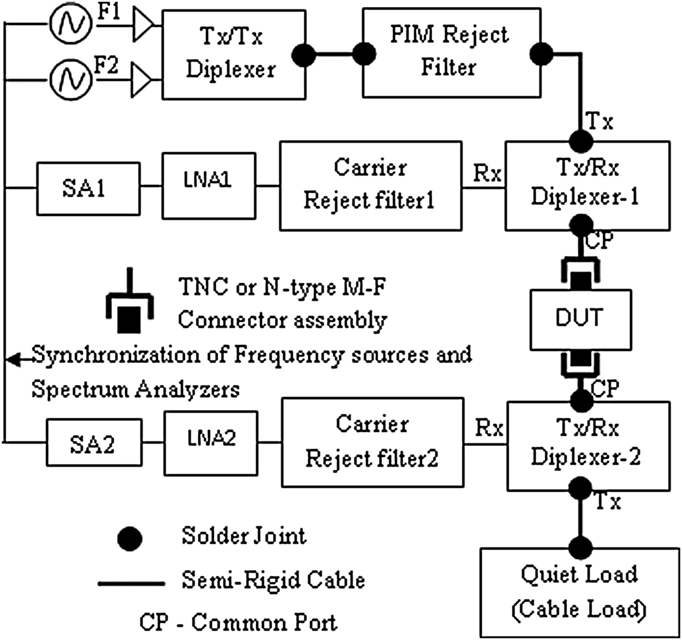
The block diagram of an ideal test setup for PIM measurement of sub-systems operating at UHF band is shown in Fig. 1.

Fig. 1. Block diagram of an ideal test setup for PIM measurement.
The criticalities involved in the development of the setup are
A) PIM performance of connectors and flexible cables
The connectors and flexible cables, themselves have a PIM performance of −90 dBm. Flexible cables have braided outer conductor due to which their PIM performance is poor as compared to semi rigid (SR) cables, which have solid outer conductor. This calls for connector-less inter-connection of the sub-systems of the setup using SR cables soldered at respective ports which itself is a challenging task.
B) Fabrication and surface treatment
From the PIM performance point of view, the sub-systems of the setup are to be fabricated, to the possible extent in a single piece. When realized in pieces, they are to be integrated with pressure joints. Depending on the base material, the sub-systems are to be subjected to a surface treatment (silver plating) of a few tens of microns (minimum of 20–25 µm for aluminum) at UHF frequencies. This thickness is to be uniform over the whole surface of the component essentially at high current density regions. Copper that has linear characteristics and good electrical conductivity can be used as the base material for realization of the sub-systems and they can be used without silver plating.
C) PIM Performance of high power termination
The conventional high power terminations make use of dissipative elements that have poor PIM performance. Quiet loads are essential for the PIM measurement setup. A cable load has good PIM performance.
All the sub-systems between the multi-carrier origin and termination point are to be inter-connected using SR cables soldered at respective ports. The PIM generated at a point in the DUT consists of forward PIM that travels in forward direction and reverse PIM or reflective PIM that travels in the reverse direction. The PIM performance of one-port devices is evaluated by measuring the reflective PIM, whereas two-port devices can be evaluated by measuring either forward or reflective PIM. A PIM test setup shall be configured for both reflective and forward PIM measurements, so that it need not be reconfigured whether it is a one-port or two-port device.
Tx/Tx diplexer is used to combine two high power carriers. PIM reject filter is used to suppress PIM generated by Tx/Tx diplexer. Tx/Rx diplexer-1 separates reflective PIM of the DUT from carrier while Tx/Rx diplexer-2 separates forward PIM of the DUT from the carrier. The carrier reject filters are used to suppress the carriers in the receive channel, so that the low noise amplifier(s) (LNA(s)) do not get saturated. Spectrum analyzers SA1 and SA2 measure reflective and forward PIM of the DUT, respectively.
The termination that dissipates the carrier power should be a quiet load (low PIM) [Reference Antkowiak and Schraufnagl5], which is usually a cable load. It consists of an absorptive cable designed for optimal PIM characteristics and required attenuation of carrier power. The loss of the cable is directly proportional to its length and inversely proportional to its diameter. The power handling of the cable depends on the diameter of the cable. Quarter-inch SR cable is an ideal choice for the quiet load for its good PIM performance and in achieving the required attenuation in shorter length of the cable. The cable is sized such that when the maximum RF power to be terminated is injected into it, the power gets entirely dissipated in the cable before reaching the other end of the cable. If the power is not entirely dissipated in the cable, the far end of the cable that is left open reflects the signal back into the cable and gets dissipated in the cable as a reflected signal. A typical quarter-inch SR cable has a loss of 0.1 dB/m.
For a quiet load with required return loss of 30 dB, a minimum of 150 m length quarter-inch SR cable is required, so that the injected power gets attenuated by 15 dB each in forward path and return path. The input of the quiet load should be directly soldered at Tx port of Tx/Rx diplexer-2 of the test setup.
All the sub-systems falling in the multi-carrier path, to the possible extent shall be realized in single-piece construction for better PIM performance of the system.
They shall be realized using metals such as copper that has linear characteristics, as the base material. The added advantage is the homogeneity of the materials as the SR cables are also made of Be–Cu. Also sub-systems made of copper can be used without silver plating as copper has good electric conductivity. At UHF band, for components made of aluminum, a minimum of 20 µm of silver plating is required for 99% of the current to be concentrated inside silver. Uniform deposition of silver of 20 µm thickness throughout the surface (essentially at high current density regions) of the filter cavity is very difficult. If sub-systems are realized using copper, then silver-plating issues can be avoided. They shall be realized without any tuning screws. Tuning screws, if used, shall be either pressure bolted or soldered [Reference Radcliffe6]. Lead free solder material (such as Sn-96) shall be selected.
The DUT as shown in Fig. 1 may or may not have connectors at both input and output ports. Necessary changes in the setup are to be made so as to mate with the DUT's ports. Irrespective of the type of the DUT's ports, the setup's PIM level is measured without any mated connectors in the through path.
III. PROPOSED SETUP FOR PIM MEASUREMENT
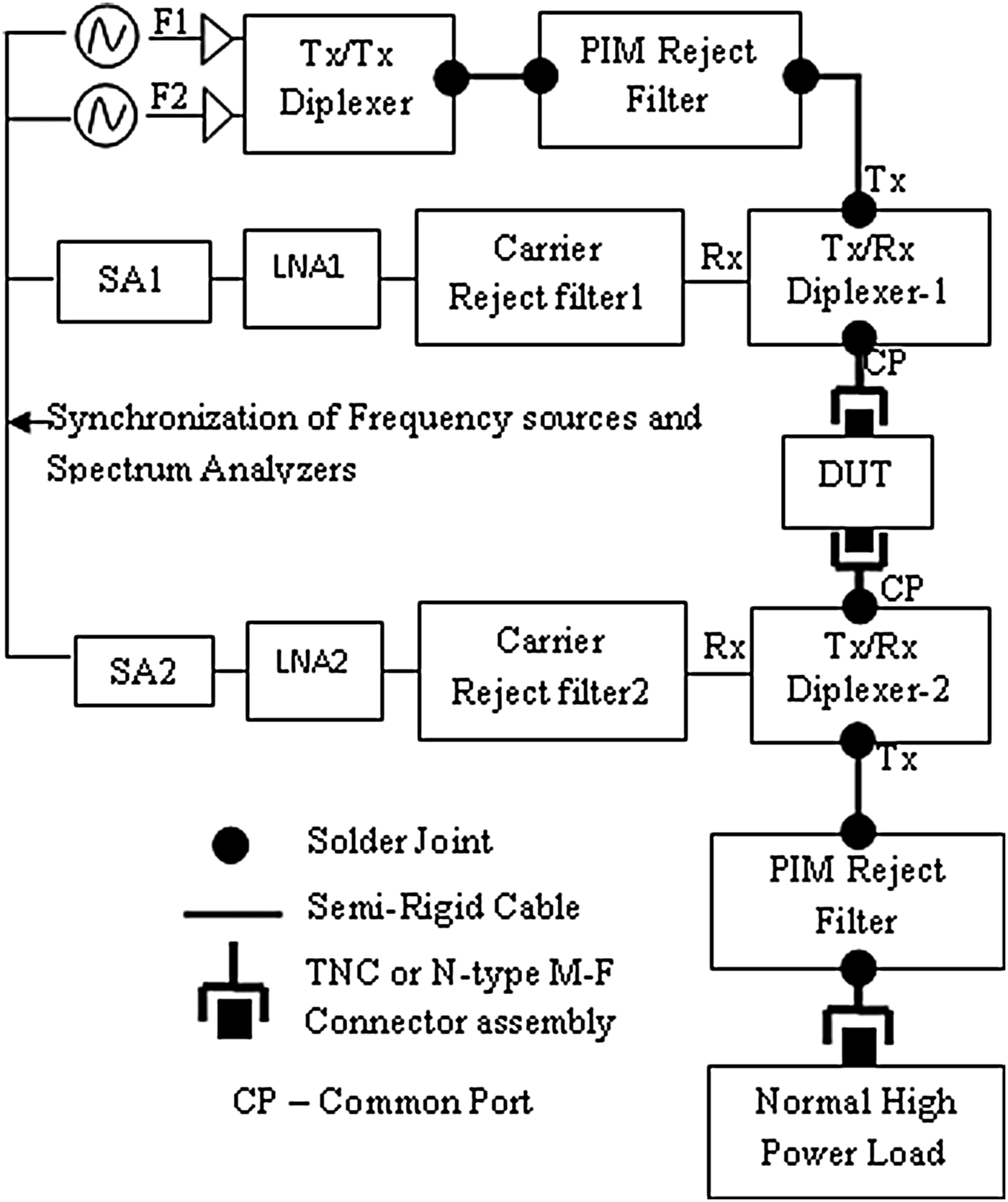
The quiet load shown in Fig. 1 is an SR cable lengthy enough to attenuate the carrier power. Such a lengthy cable may not be readily available. A setup for PIM measurement using a readily available normal high power load but still having the performance close to that of the ideal one is proposed and the block diagram of the same is shown in Fig. 2.
Fig. 2. Block diagram of proposed test setup for PIM measurement.
The proposed setup differs from the ideal one in the high power load and the introduction of PIM reject filter between Tx/Rx diplexer-2 and load. A normal high power load with a TNC/N-type connector can be used along with a PIM reject filter, which suppresses the PIM generated by the dissipative elements of the load and the connector assembly. The PIM reject filter in combination with the Tx channel of the Tx/Rx diplexer-2 should provide rejection better than 100 dB for Rx frequencies, so that the PIM generated by the load (approx. −90 dBm.) is well below the thermal noise of LNA2.
A) Design details
1) TX/TX DIPLEXER
This is used to combine two carriers to generate a two-tone signal. The two carrier frequencies are 243.955 and 254.15 MHz with 100 W power per carrier. The Diplexer consists of two four-pole Chebyschev coaxial resonator filters each of 4 MHz bandwidth, combined using a common transformer. The input couplings for both the channels are realized using transformers. TNC-F connectors are used at both the channel inputs, whereas SR cable is soldered to the transformer at the common port so as to have connector-less joint in the multi-carrier path. The diplexer is made of aluminum alloy and has been silver plated internally. It consists of a filter box with integrated resonator rods and top cover. The bottom of the cavities near the corners and the short-circuited portion of the resonators are provided with radius [Reference Radcliffe6, Reference Macchiarella and Sartorio7] to ensure proper silver plating. The diplexer has isolation better than 40 dB between the channels.
2) PIM REJECT FILTER
This is used to suppress the PIM generated by the Tx/Tx diplexer and provide a PIM-free two-tone signal as an input to the DUT. A minimum of 60 dB rejection is necessary to provide PIM-free signal to the DUT. The filter can be realized either as a coaxial stepped impedance low-pass filter or as a band-stop filter. For a given number of sections, a band-stop filter is compact and provides more rejection than the low-pass filter in the required stop-band. For the test setup, the PIM reject filter has been realized as a four-pole band-stop filter using short-circuited stubs [Reference Hong and Lancaster8] in strip-line. The filter is completely loaded with Teflon to make it compact. It has a pass-band: 242.1–254.7 MHz with a minimum rejection of 35 dB in the stop-band: 289–321 MHz. A cascade of 3 identical PIM reject filters has been used in the setup, so that the PIM generated by the Tx/Tx diplexer gets suppressed by a minimum of 105 dB. Another cascade of three such filters is also used at the output of the setup between load and Tx port of the Tx/Rx diplexer-2 to suppress the PIM generated by the load.
3) TX/RX DIPLEXER
It is used to separate the carrier power and the PIM generated by the DUT. It consists of two seven-pole Chebyschev inter-digital filters combined using a common transformer. The Tx channel has pass-band: 236–264 MHz, whereas the Rx channel has 289–321 MHz. SR cable at the Tx port and TNC-F connector at the Rx port are soldered to the respective transformers used for external coupling realization. It consists of a filter box with integrated resonator rods and transformers, top cover and bottom cover – all made of silver-plated aluminum alloy. The mating areas have been provided with pressure ridges. The resonator rods and external transformers are square in cross-section, whereas common transformer is rectangular in cross-section to ease the fabrication of the box with these integrated rods. The radius at the short-circuited region of the rods not only eases the fabrication but also ensures proper plating of the surface [Reference Radcliffe6, Reference Macchiarella and Sartorio7]. It has been realized without using any tuning screws. The diplexer has isolation better than 70 dB between the channels. The established setup was intended for forward PIM measurement of the DUT and hence only one diplexer was developed.
4) CARRIER REJECT FILTER
This is used to suppress the carrier sufficient enough to avoid saturation of the LNA. This has been realized using helical resonators. The filter provides a rejection better than 100 dB at Tx frequencies. For a 50 dBm carrier input, the carrier power level at the Rx port of Tx/Rx diplexer will be −12 dBm. The carrier reject filter further suppresses it to −112 dBm.
5) JUNCTION BOX
This is a 50 Ω strip-line used for interconnecting two SR cables. It consists of an inner conductor, an outer casing both made of oxidation-free high conductivity (OFHC) copper and Teflon between the inner and outer conductors. The surfaces of the components made of ordinary copper get oxidized over a period of time resulting in degradation of PIM performance of the setup. Teflon loading is done to make the junction box compact. The photographs of the realized sub-systems of the setup and their measured results are shown in Figs 3 and 4, respectively.
Fig. 3. (a) Photograph of Tx/Tx diplexer. (b) Photograph of Tx/Rx diplexer. (c) Photograph of PIM reject filter and junction box assembly. (d) Photograph of carrier reject filter.
Fig. 4. (a) Measured results of Tx/Tx diplexer. (b) Measured results of Tx/Rx diplexer. (c) Measured results of PIM reject filter–junction box assembly. (d) Measured results of carrier reject filter.
IV. ESTABLISHMENT OF THE PIM TEST SETUP
The established PIM test setup was intended for the measurement of PIM performance of two-port devices. Also it takes lots of efforts and resources in realization of a huge structure such as Tx/Rx diplexer. Only one Tx/Rx diplexer was developed and the setup was configured for forward PIM measurement of a two-port DUT. The photograph of the established PIM test setup is shown in Fig. 5.
Fig. 5. Photograph of the PIM test setup – through configuration.
The SR cables used for interconnecting the sub-systems are subjected to stress relieving cycle so as to release the stresses developed because of mechanical operations such as bending, cutting etc., performed on cables for preparing them as per the required layout. All the sub-systems are mounted on a flat surface and care is taken for supporting the cables, so that all the joints are stress-free. The diplexers of the setup were made of aluminum instead of copper due to non-availability of huge blocks of copper required for fabrication of these sub-systems in single piece. The surface treatment process used for silver plating the aluminum components is qualified up to 200°C. Beyond this temperature, silver deposited on aluminum gets peeled off. Owing to this surface treatment process limitation, Sn-63/Pb-37(melting point of 183°C) instead of Sn-96(melting point of 220°C) was used for soldering. Soldering of the SR cable ends toward the sub-systems with huge thermal mass is done by placing them on a hot-plate. The sub-systems are inter-connected by soldering respective cables at the ports of junction box.
Two carriers, 243.955 and 254.15 MHz, each of 100 W power are fed to the Tx/Tx diplexer of the setup and PIM performance of the setup is measured.
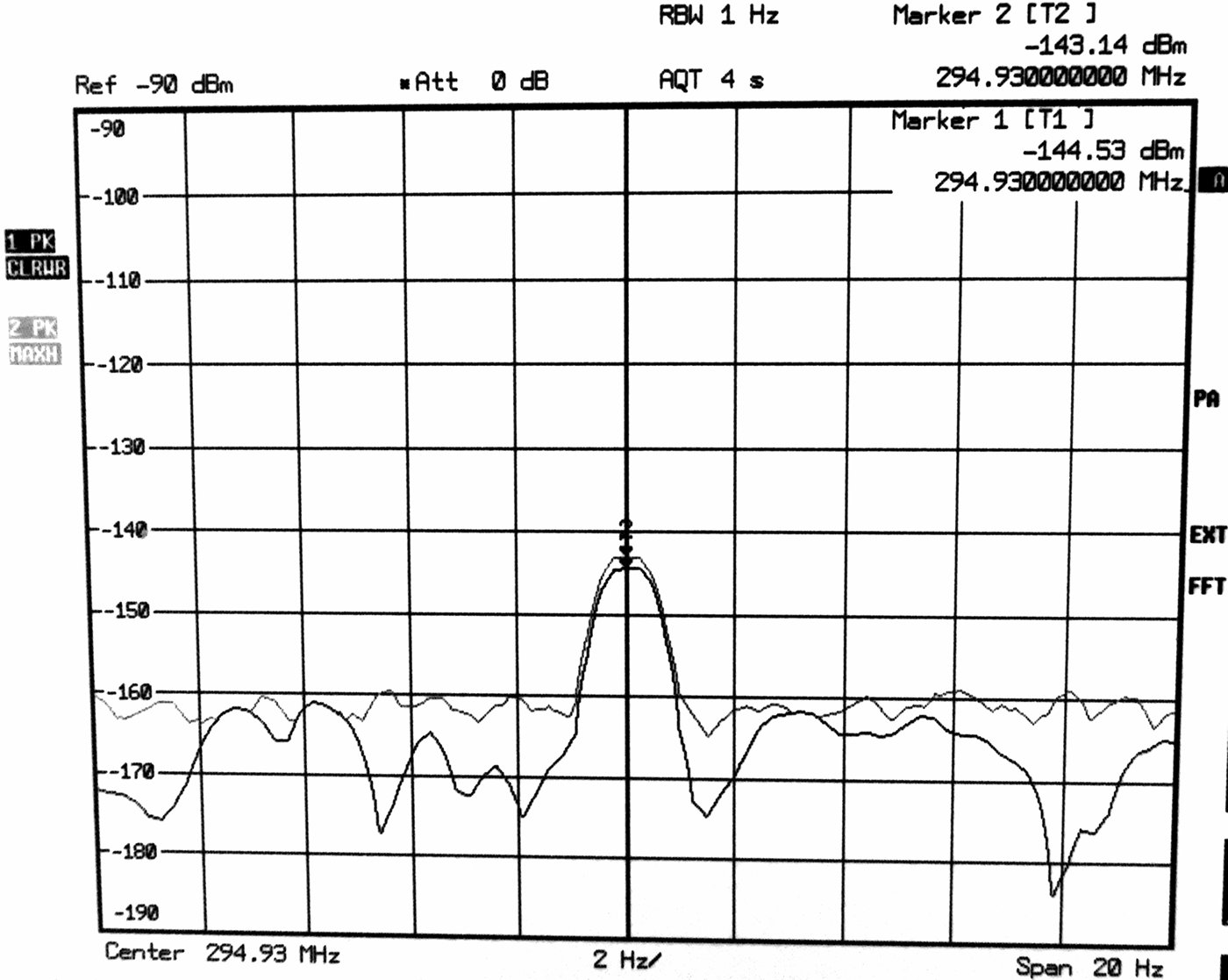
The measured PIM level is the algebraic sum of Spectrum Analyzer reading and losses between Tx/Rx diplexer and Spectrum Analyzer. The measured ninth-order PIM level at 294.93 MHz was found to be −142 dBm (−143.14 + 1.3 = −141.84 dBm ≈−142 dBm) and the same is shown in Fig. 6.
Fig. 6. Measured PIM level of the setup.
V. PIM MEASUREMENT OF DUT
The established test setup was used for measuring the PIM performance of the following Devices:
DUT1 – four-pole band-stop filter (Qualification Model).
DUT2 – four-pole band-stop filter (Spare unit)
DUT3 – four-pole band-stop filter (Flight Model).
DUT4 – A flexible cable
DUT5 – Cascade of band-stop filter and flexible cable
A ninth-order PIM at 294.93 MHz is measured for all the above devices with two input carriers: 243.955 and 254.15 MHz each of 100 W power.
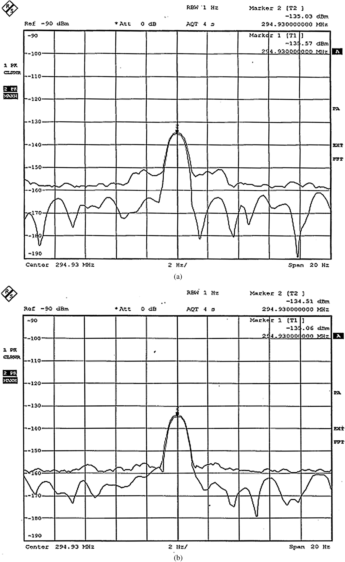
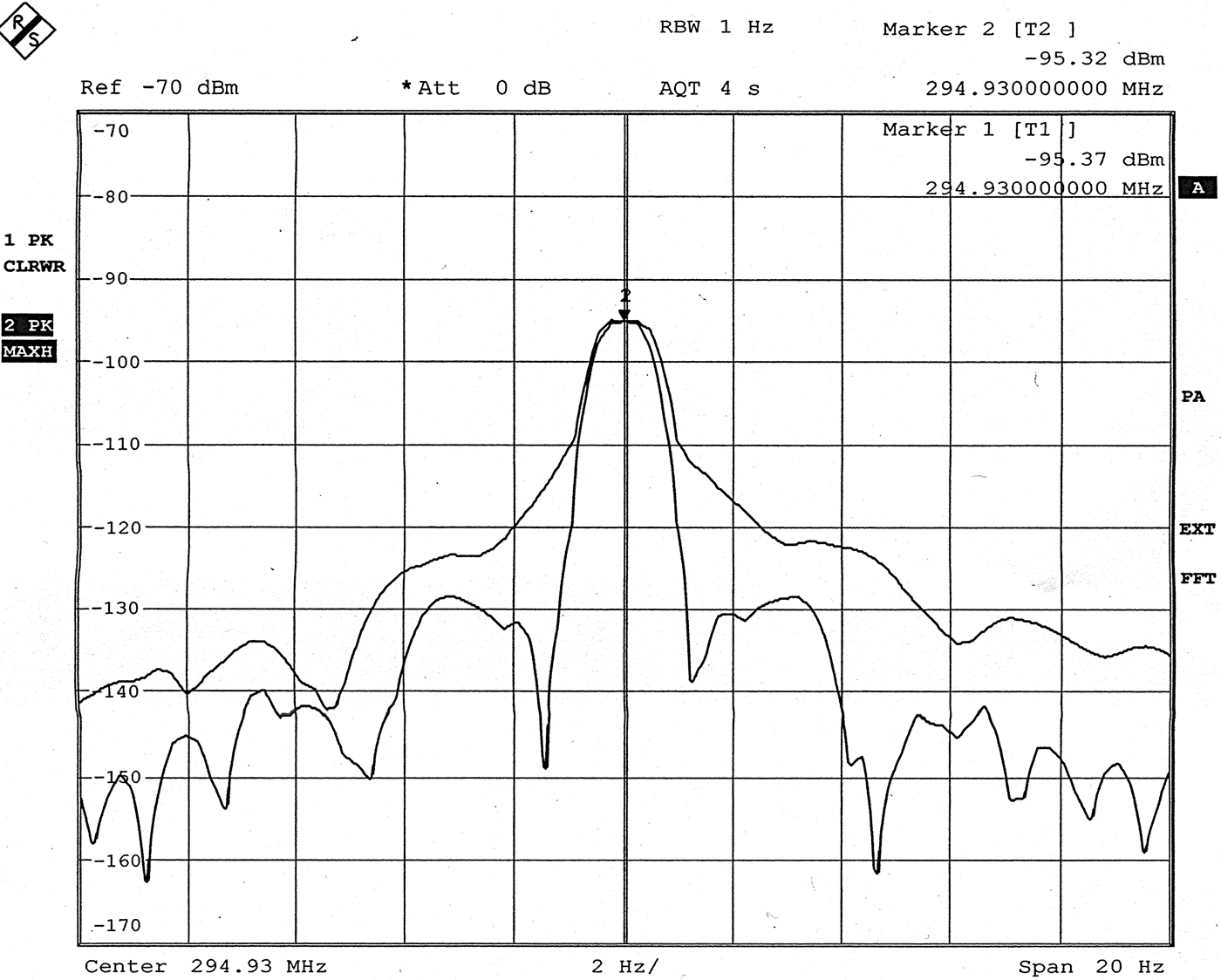
The DUT1 is a four-pole band-stop filter–junction box assembly identical to the PIM reject filter used in the setup, except for the TNC-F connector at the input port. The photograph of the test setup with DUT1 connected is shown in Fig. 7. The measured PIM levels of DUT1 are shown in Fig. 8. The PIM performance was observed for duration of 1 h each at ambient temperature and 85°C. Trace 2 (T2) in the plots gives the worst-case PIM level over the period of observation. The PIM level was stable over temperature and time.
Fig. 7. Photograph of the PIM test setup with DUT1.
Fig. 8. (a) PIM level of DUT1 measured at ambient temperature. (b) PIM level of DUT1 measured at 85°C.
DUT2 and DUT3 are identical to DUT1 except for the difference in the extreme temperatures at which they are to be tested.
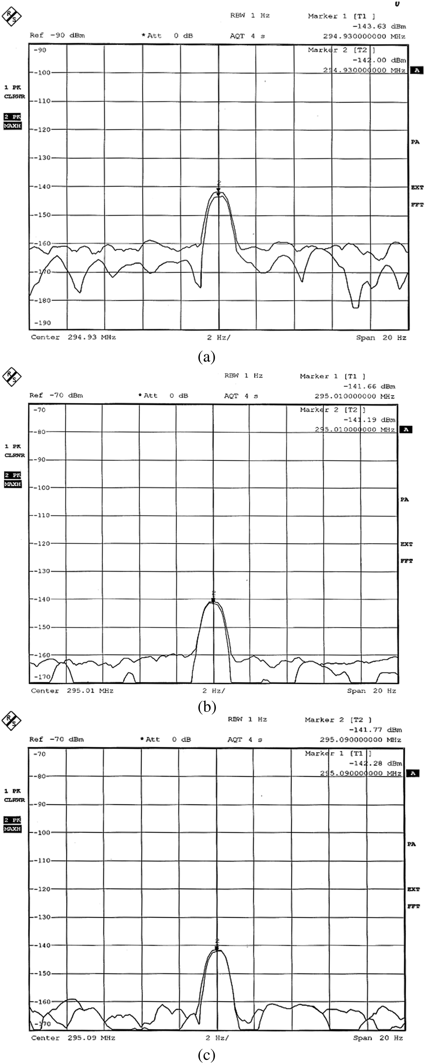
DUT4 is a flexible cable, which will be used at the input of DUT3 in the payload. The PIM performance of the DUT4 was measured and the results are shown in Fig. 9.
Fig. 9. Measured PIM level of DUT4.
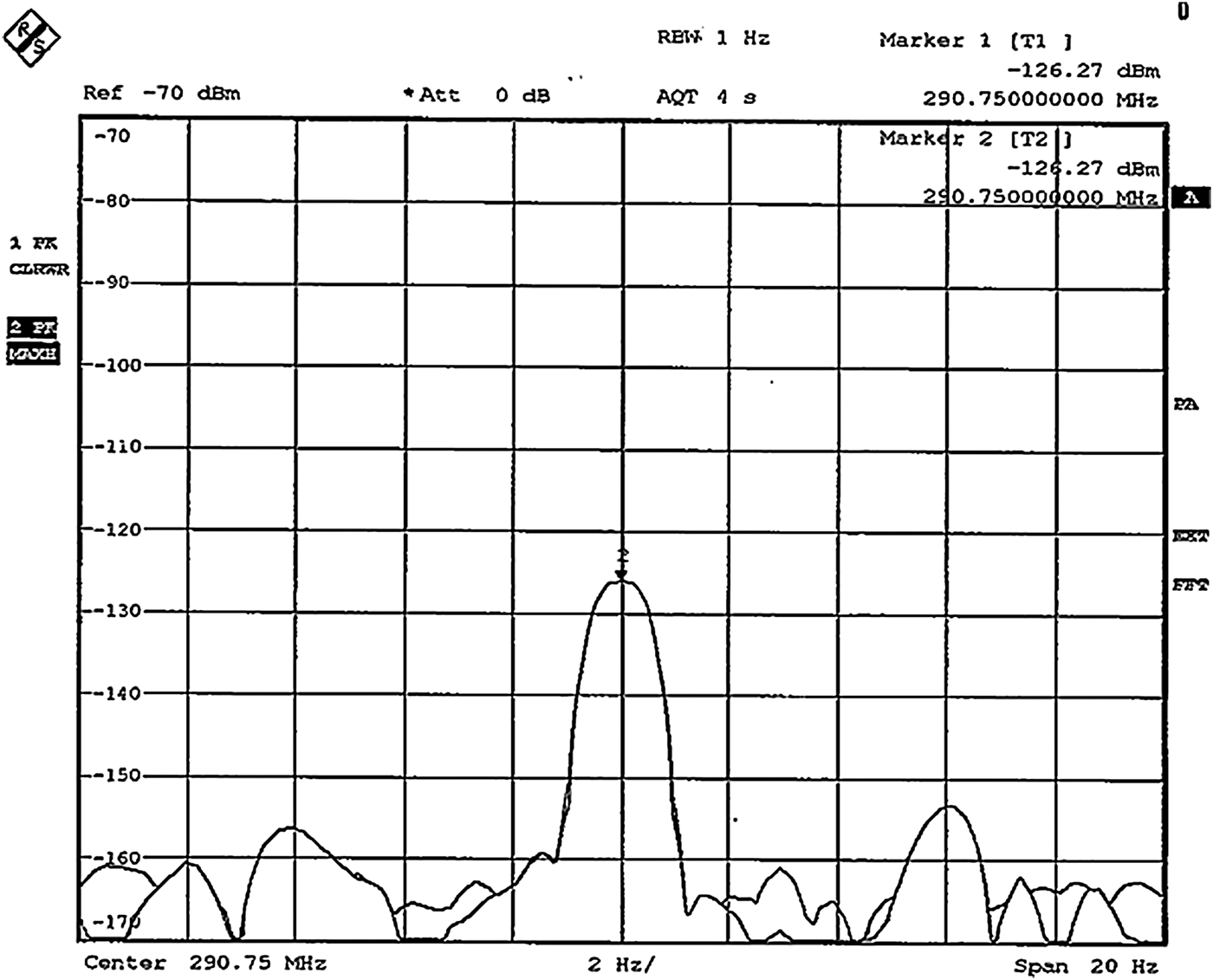
DUT5 that is a cascade of a flexible cable and band-stop filter was tested for PIM performance. The photograph of the setup with this DUT5 is shown in Fig. 10.
Fig. 10. Photograph of the PIM test setup with DUT5.
The PIM level of the band-stop filter was measured to be −135 dBm. The PIM level of the cascade of flexible cable and band-stop filter is expected to be either same as that of the band-stop filter (if its rejection is enough to suppress the PIM generated by the cable) or higher than that of the band-stop filter (if its rejection is not enough to suppress the PIM generated by the cable). Surprisingly, the measured PIM level of the cascade was found to be <−140 dBm, which is better than the PIM level of the standalone band-stop filter.
The test was repeated by shifting one of the carrier frequencies lower in steps of 20 kHz to 243.935MHz and 243.915 MHz, keeping the other carrier at 254.15 MHz. In both the cases the PIM level was <−140 dBm. The measured PIM levels with three different frequencies are shown in Fig. 11.
Fig. 11. (a) PIM level of DUT5 measured with input carrier frequencies 254.15 and 243.955 MHz. (b) PIM level of DUT5 measured with input carrier frequencies 254.15 and 243.935 MHz. (c) PIM level of DUT5 measured with input carrier frequencies 254.15 and 243.915 MHz.
The carrier was then shifted to 245 MHz keeping the other carrier frequency at 254.15 MHz. The PIM level was found to be −126 dBm and the plot is shown in Fig. 12. This confirms that the PIM cancellation [Reference Henrie, Christianson and Chappell9] is taking place specifically at 243.955 MHz.
Fig. 12. PIM level of DUT5 measured with input carrier frequencies 254.15 and 245 MHz
With one of the carriers fixed at 254.15 MHz and the other carrier at 243.915, 243.935 and 243.955 MHz, the PIM level of the flexible cable is −96 dBm and that of band-stop filter is −135 dBm. The rejection provided by the band-stop filter at the corresponding PIM frequencies is 36.5 dB. When the flexible cable and the band-stop filter are connected in cascade, the band-stop filter suppresses PIM generated by the flexible cable (−96 dBm) by 36.5 dB resulting in a PIM (flexible cable's contribution) level of −133 dBm at the output of the band-stop filter. The band-stop filter itself puts a PIM of −135 dBm at its output. Since the PIM contributions of both flexible cable and band-stop filter at DUT-5's output are closer in magnitude, there is a chance of them getting cancelled depending upon their phase. DUT5's measured PIM level of −141 dBm which is close to setup's PIM level proves the cancellation of PIM.
With the carriers 245 and 254.15 MHz, the PIM level of the flexible cable is 90 dBm and that of band-stop filter is 135 dBm. The rejection provided by the band-stop at the corresponding PIM frequency is 35.4 dB. When cascaded, the PIM contributions of flexible cable and the band-stop filter at the output are −125 and −135 dBm, respectively. Since the magnitudes are not closer, the net PIM level will be closer to the highest of the individual PIM contributions. The same was observed in the measurement which shows a PIM level of −125 dBm.
The measured PIM levels of all the devices are tabulated in Table 1.
Table 1. Measured PIM levels of all the devices under test.
Scope for improvement in the measurement test setup
1. The PIM reject filter bank which consists of three filters connected in cascade can be replaced by a single filter that provides the rejection same as that of the filter bank. This reduces the no. of solder joints in the setup, thus improving the PIM level of the setup.
2. The Tx/Tx diplexer and Tx/Rx diplexer can be realized using a single copper block, so that they can be used without silver plating, avoiding the problems associated with silver plating of such huge structures. The Tx/Rx diplexer made of copper in [Reference Radcliffe6] has a seventh-order PIM level of −160 dBm at 260 W carrier power.
3. Soldering material Sn-96 (Sn: 96%, Ag: 3.2%, and Cu: 0.8%) having better PIM performance than Sn-63, can be used. Sn-96 has a melting point of 220°C.
With these modifications PIM level can be further improved. If quiet load is available, it is recommended to use it, so that PIM reject filter between the load and Tx/Rx diplexer can be eliminated.
VI. CONCLUSION
A connector-less PIM measurement test setup at UHF band, without a quiet load is established and achieved a ninth-order PIM level of −142 dBm. PIM performance (ninth order) of DUTs – four-pole band-stop filter, flexible cable and a cascade of band-stop filter and flexible cable is characterized using the established setup.
Flexible cables and connectors have ninth-order PIM level of −90 dBm and hence cannot be used in test setups for measuring PIM levels better than −90 dBm. A combination of high power load and PIM reject filter can be used in case quiet load is not readily available.
The reported connector-less solution can also be used for PIM characterization of planar contacts, printed antenna etc.
ACKNOWLEDGEMENTS
The authors are grateful to the Director, Space Applications Centre (ISRO) and Deputy Director, SNPA for their support throughout the work. The authors would like to thank Mr. Hitesh Modi, Mr. Vikrant Singh and Ms. Shilpi Soni for their support in the electrical design of test setup components. The authors also thank Mr. K. Karthik for his valuable inputs and support in the mechanical design of the setup components.
 Santhosh Kumar Ramagiri received the Bachelor of Engineering in Electronics and Communication from Osmania University, Hyderabad, India in 2002. From 2002 to 2004, he worked as a Faculty at M.V.S.R Engineering College, Hyderabad, India with specialization in Signals and Systems. From 2004 to 2005, he worked as a Software Engineer at Brahmos Aerospace Pvt. Ltd., Hyderabad, India. He joined the Space Applications Centre of Indian Space Research Organisation as an RF and Microwave engineer in 2005. He was involved in design and development of high power passive microwave components such as filters, diplexers, harmonic reject filters, PIM reject filters, and output hybrid networks for satellite communication and navigation payloads. He has developed various types of filters and diplexers for Multipaction and PIM test setups in UHF, S, C, Ku, and Ka-bands. His current efforts continue to focus on development of novel harmonic reject filters, filters in Q/V band and reconfigurable filters.
 Arvind B. Shukla received the Diploma in Electronics and Radio Engineering from Gujarat Technical Education Board, Gujarat, India in 1977. He joined the Space Applications Centre of Indian Space Research Organisation as a Technical Assistant in 1978. He received the Bachelor of Engineering in Electronics and Communication from Gujarat University, Ahmedabad, India in 1983. He was involved in design and development of passive microwave components such as input multiplexers, harmonic reject filters, and PIM reject filters. As a Deputy Project Manager and Project Manager, he was responsible for development of Output Filters and Multiplexers for various satellite communication payloads. Currently he is involved in the development of novel harmonic reject filters.
 Ramaniklal B. Bavaria received the Diploma in Electronics and Radio Engineering from Gujarat Technical Education Board, Gujarat, India in 1976. He joined the Space Applications Centre of Indian Space Research Organisation as a Technical Assistant in 1977. He received Bachelor of Engineering in Electronics & Communication from Gujarat University, Ahmedabad, India in 1985. He was involved in the design, development, and space qualification of satellite payload components for communication satellites. He was involved in the development of Antennae for INSAT series of satellites. He was also responsible for the development of passive microwave components such as Input and Output Multiplexers, high power microwave components such as filters, couplers, diplexers, and harmonic reject filters for satellite communication and navigation payloads. He has served as Head of Payload Filters Division from 2010 to 2013.
 Surinder Singh completed his Master of Technology in Microwave Electronics from Delhi University in 1986 and joined the Space Applications Centre, Indian Space Research Organisation, Ahmedabad, India. He has worked on the design and delivery of the space borne hardware for more than 25 years. He has worked on many cutting edge technologies such as MMIC, RF MEMS, Dielectric Resonator filters, High Temperature Superconducting Filters to realize Reliable, Compact and Light Weight subsystems for SATCOM and Navigation payloads. The systems developed by him for on-board applications include low noise amplifiers, up and down converters, receivers, input multiplexers, narrowband filters, multiple pass band filters, and pre-select filters.
Kaushik S. Parikh received the Bachelor of Engineering in Electronics and Communication in 1986. He joined the Space Applications Centre, Indian Space Research Organisation (ISRO), India as an RF and Microwave engineer. He was involved in the design, development and space qualification of satellite payload components for communication satellites. He was involved in the development of RF front end receivers Beacon transmitters for INSAT series of satellites. He was also responsible for the development of passive microwave components such as Input and Output Multiplexers, high power microwave components such as filters, couplers, diplexers, and harmonic reject filters for satellite communication payload. He was instrumental for the establishment of high power test facility for conducting Multipaction, PIM and Corona tests on payload components. Currently he is working for the development of satcom ground terminals for mobile satellite service and navigation user receiver for IRNSS navigation system and is the Deputy Director of Satcom and Navigation Applications Area.