


Introduction
Recent advancements in the field of microwave circuits require compact bandpass filters with low loss and wide-stopband performance. Metal waveguides are widely used to design high-performance bandpass filters due to their excellent Q-factor and low loss characteristics. However, they are of large volume and high cost, and it is difficult to integrate them with planar microwave circuits. Substrate integrated waveguide (SIW) is a good candidate for the design of microwave circuits due to their advantages such as small size, light weight and low cost [Reference Deslandes and Wu1]. Various microwave filters have been designed using SIW cavities. However, the higher-order modes of the SIW cavity degrade the stopband performance of the filters. A number of methods have been adopted to realize SIW filters with wide-stopband performance. The feed design technique and coupling scheme in multilayer structures are proposed to suppress undesired higher-order modes of the cavity, and wide-stopband is obtained [Reference Lee, Lee, Lee, Uhm and Lee2, Reference Jia, Feng, Xiang and Wu3]. Compared to multilayer structures, single-layer structures exhibit low cost and ease of fabrication. Single-layer SIW bandpass filters with wide-stopband characteristic are reported [Reference Chen, Wu and Drolet4–Reference Zhou, Zhou and Wu7]. Since the filters are composed of several SIW rectangular cavities whose size is larger than that of square cavity for identical fundamental frequency, the overall filter size is large. In order to reduce the filter size, half-mode SIW, quarter-mode SIW, eighth-mode SIW, and sixteenth-mode SIW cavity filters with improved out-of-band rejection are reported [Reference Shen8–Reference Azad and Mohan11]. Although, significant size reduction is achieved, the unloaded Q-factors of the reported cavities are small compared to that of the SIW cavity. Another size reduction scheme is developed by combining SIW and planar resonators, and compact filters are realized [Reference Shen, Yin, Sun and Wu12–Reference Shen, Yin, Sun and Mao14]. SIW and microstrip lines are combined to design compact bandpass filters in [Reference Shen, Yin, Sun and Wu12] whereas SIW and coplanar waveguide (CPW) are utilized to realize compact filters in [Reference Chu, Hong, Dai, Tang, Chen, Hao, Zhu and Wu13]. However, the demonstrated filters exhibit compact size due to combination of SIW and planar resonators, but they are not designed for wide-stopband performance. A compact bandpass filter with wide-stopband characteristic using SIW and CPW is presented in [Reference Shen, Yin, Sun and Mao14], but the bandwidth is limited to only 6%.
Recently, a two-pole SIW bandpass filter with wide-stopband performance is reported [Reference Azad and Mohan15]. A short-circuited coplanar line is introduced between two SIW cavities to realize the desired couplings of TE101 and TE102 modes of the SIW cavity. The coupling coefficients of the two modes are controlled by adjusting the width of the short-circuited coplanar line and the width of the iris-window between the two cavities. The passband is produced by the TE101 modes of the SIW cavity, and its bandwidth is controlled by adjusting the coupling of TE101 mode. Moreover, the coupling of TE102 mode is minimized, and the passband generated by the TE102 mode is suppressed in order to obtain wide-stopband performance. However, the filter has good stopband characteristic, the limited available range of TE101 coupling leads to narrow-band design.
In this article, the approach presented in [Reference Azad and Mohan15] is extended to design a compact wideband bandpass filter with wide-stopband rejection, and the bandwidth limitation of the filter reported in [Reference Azad and Mohan15] is eliminated. Here, the short-circuited coplanar line introduced between the two SIW cavities is not only used to control the coupling of TE101 and TE102 modes of the cavity, but also acts as a resonator. The fundamental resonant frequency of the short-circuited coplanar line is adjusted and combined with the resonant frequency of TE101 mode of the SIW cavities to design a three-pole filter. In addition, the coupling of TE102 mode is minimized, and the passband generated at the resonant frequency of TE102 mode is suppressed in order to obtain wide-stopband performance. Moreover, the center frequency (CF) and the bandwidth of the filter can be controlled by adjusting the geometrical parameters such as the dimensions of the SIW cavities, dimensions of the short-circuited coplanar line, and the width of the iris-window. A third-order bandpass filter with a wide-stopband is designed to operate at 10 GHz with a 3-dB fractional bandwidth (FBW) of 17.5%, and it is fabricated and measured for validation purpose. Moreover, the simulation and measurement results agree well with each other. The size of the proposed filter is reduced by a factor of 1/2 compared to SIW filters in triplet configuration, and 1/3 in comparison with inline SIW filters. Simple structure, compact size, wide bandwidth, low loss, and wide-stopband rejection are the advantages of the proposed filter. The filter is a suitable candidate for radar systems and satellite communication applications.
Filter analysis and design
Figure 1(a) shows the structure of a conventional two-pole SIW bandpass filter. Two SIW cavities are coupled through an iris-window to produce a passband. Its simulated S-parameters are presented in Fig. 1(b). It is seen that the TE101 modes of the cavity generate a passband at 10 GHz while the second passband is created at 15.6 GHz due to the first higher-order mode TE102 of the cavity. The simulated E-field distributions in the filter at 10 GHz (f 101) and 15.6 GHz (f 102) are plotted in Figs 2(a) and 2(b), respectively. It can be seen that the first passband is created by TE101 mode of the cavities while the second passband is generated by the TE102 mode of the cavities which degrades the stopband performance of the filter. The stopband performance can be improved by suppressing the passband constituted by TE102 modes.
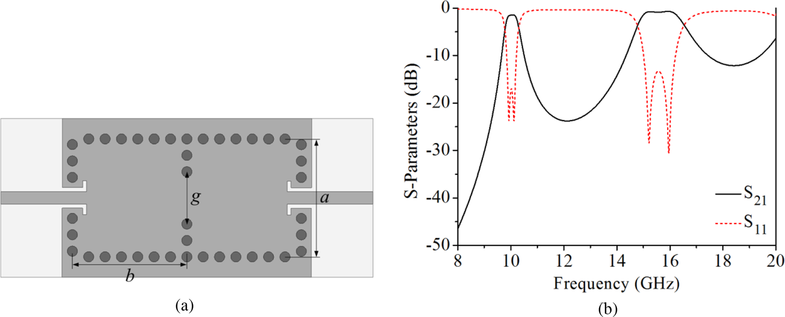
Fig. 1. (a) Structure of a conventional two-pole SIW bandpass filter (a = 11.5 mm, b = 11.2 mm, and g = 5.1 mm) and (b) simulated S-parameters.

Fig. 2. Simulated E-field distributions in the filter at (a) 10 GHz (f 101) and (b) 15.6 GHz (f 102).
The configuration of the proposed compact SIW bandpass filter with a wide-stopband is illustrated in Fig. 3. A short-circuited coplanar line is introduced between two SIW cavities [Reference Azad and Mohan15]. The iris-window between the two SIW cavities produces magnetic coupling of TE101 and TE102 modes of the cavity, whereas the electric coupling of these two modes is generated by the short-circuited coplanar line, as discussed in [Reference Azad and Mohan15]. Thus, the overall couplings of TE101 and TE102 modes are mixed coupling, and the coupling of the two modes can be controlled by adjusting the width of the iris-window (g), the length (l), and the width (w 4) of the short-circuited coplanar line. The passband created by the TE102 mode of the cavity can be suppressed by minimizing the coupling of TE102 mode.

Fig. 3. Configuration of the proposed compact SIW bandpass filter with wide-stopband performance.
In this work, the short-circuited coplanar line is not only used to control the coupling of the two modes of the cavity, but also acts as a resonator. The resonant frequencies of the TE101 mode of SIW cavities (f 1 and f 2) and the fundamental resonant frequency of the short-circuited coplanar line (f 3) can be adjusted to constitute a third-order filter response. The initial dimensions of the SIW cavity resonating at its fundamental resonant mode TE101 can be evaluated by using the relations:
 $$\eqalign{&f_{{\rm TE}101} = \displaystyle{c \over {2\sqrt {\varepsilon _r}}} \sqrt {{\left( {\displaystyle{1 \over {a_e}}} \right)}^2 + {\left( {\displaystyle{1 \over {b_e}}} \right)}^2}; \cr &a_e = a-\displaystyle{{d^2} \over {0.95p}},\quad b_e = b-\displaystyle{{d^2} \over {0.95p}}$$
where c is the speed of light in vacuum, ɛ r is the dielectric constant of the substrate, d is the diameter of the metalized via-holes and p is the center-to-center spacing between the via-holes. Furthermore, the fundamental resonant frequency of the short-circuited coplanar line can be approximately determined by using the relation:
 $$f_3\simeq \displaystyle{c \over {2l\sqrt {\varepsilon _{re}}}} $$
where l is the length of the short-circuited coplanar line resonator and ɛ re is the effective dielectric constant of the substrate which depends on the width of the short-circuited coplanar line and the height of the substrate. The resonant frequencies f 1, f 2, and f 3 are determined for desired CF and bandwidth of the filter. The size of the proposed filter is very compact compared to conventional third-order SIW filters. The filter is designed on the Rogers RO4003C substrate with ɛ r = 3.55, h = 0.508 mm, and tan δ = 0.0027. The metalized via-holes have d = 1 mm and p = 1.6 mm. Full-wave EM simulator Ansoft HFSS is used to perform the analysis and design of the filter.
The simulated S-parameters of the proposed filter under the condition of weak I/O coupling are shown in Fig. 4. The dimensions of the filter in the simulation are: a = 11.25, b = 11.2, wf = 1.2, lin = 1, lf = 3, t = 0.4, g = 4.8, l = 10.25, w 1 = 1.8, w 2 = 1.4, w 3 = 1, and w 4 = 0.2 (unit: mm). As can be seen, the resonance due to the short-circuited coplanar line (f 3) occurs at 9.29 GHz while that of the TE101 mode of the SIW cavities (f 1 and f 2) occur at 10.5 and 10.99 GHz, which illustrate that a passband can be created by adjusting the resonant frequencies f 1, f 2, and f 3 appropriately. At the same time, the passband created at 15.93 GHz due to TE102 mode of the cavities degrades the stopband attenuation of the filter, and it needs to be eliminated in order to improve the stopband performance of the filter. Figure 5 presents the simulated E-field distributions in the proposed filter at 9.29 GHz (f 3), 10.5 GHz (f 1), 10.99 GHz (f 2), and 15.93 GHz (f 102). It can be clearly observed that the first resonance is created by the short-circuited coplanar line introduced between the two SIW cavities while the second and third resonances are generated by the TE101 mode of the cavities. On the other hand, the undesired passband is generated by the TE102 mode of the cavities, and the stopband performance of the filter is degraded.

Fig. 4. Simulated S-parameters of the filter under weak coupling condition (a) |S 21| and (b) |S 11|.

Fig. 5. Simulated E-field distributions in the proposed filter at (a) 9.29 GHz (f 3), (b) 10.5 GHz (f 1), (c) 10.99 GHz (f 2), and (d) 15.93 GHz (f 102).
Figure 6 presents the simulated S-parameters of the filter against variation in g while keeping l and w 4 fixed under the condition of weak I/O coupling. The overall coupling of TE101 mode is electric dominant. The magnetic coupling decreases with a decrease in g, and the overall coupling of TE101 mode increases. This phenomenon can be verified by the graphs plotted in Fig. 6. The overall coupling of TE101 mode increases since the separation between f 1 and f 2 increases [Reference Hong and Lancaster16] as g decreases from 5.5 to 3 mm, as shown in Figs 6(a) and 6(b). On the other hand, the overall coupling of TE102 mode is magnetic dominant, and it decreases with a decrease in g. As can be seen, for g = 5.5 mm, a passband is generated at nearly 16 GHz due to TE102 mode, and it is suppressed below −18 dB when g = 3 mm, as shown in Fig. 6(a). Since f 2 increases while f 1 and f 3 remain almost constant with a decrease in g, the CF of the filter slightly shifts towards higher frequency, and the bandwidth of the filter shows a small increase. In addition, two transmission zeros (TZs) are observed at the upper stopband. The location of the first TZ shifts towards higher frequency while that of the second TZ moves towards lower frequency if g is decreased, as depicted in Fig. 6(a).

Fig. 6. Simulated S-parameters of the filter against variation in g (l = 10.25 mm and w 4 = 0.2 mm) (a) |S 21| and (b) |S 11|.
The simulated S-parameters of the filter against variation in l while maintaining constant g and w 4 are presented in Fig. 7. The overall coupling of TE101 mode is electric dominant. The magnetic coupling increases as l is increased, and the overall coupling of TE101 mode decreases. This behavior is verified by the curves presented in Fig. 7. The overall coupling of TE101 mode decreases since the separation between f 1 and f 2 decreases when l is increased from 10 to 10.5 mm, as depicted in Figs 7(a) and 7(b). However, the overall coupling of TE102 mode is magnetic dominant, and it increases with increasing l. As a result, the suppression level of the passband produced by the TE102 modes decreases slightly, still keeping below −16 dB, as shown in Fig. 7(a). Since the length of the short-circuited coplanar line l increases, f 3 decreases largely. At the same time, since f 2 slightly decreases while f 1 remains constant with an increase in l, the CF of the filter slightly moves towards lower frequency, and the bandwidth of the filter is slightly modified, as shown in Figs 7(a) and 7(b). Moreover, the positions of the TZs shift towards lower frequency as l increases, as depicted in Fig. 7(a).

Fig. 7. Simulated S-parameters of the filter against variation in l (g = 3 mm and w 4 = 0.2 mm) (a) |S 21| and (b) |S 11|.
Figure 8 depicts the simulated S-parameters of the filter against variation in w 4 while keeping fixed g and l. The overall coupling of TE101 mode is electric dominant, and it increases as w 4 is increased because the electric coupling increases with an increase in w 4. The graphs plotted in Fig. 8 verify this phenomenon. The overall coupling of TE101 mode increases slightly since the separation between f 1 and f 2 shows a slight increase as w 4 is increased from 0.2 to 0.4 mm, as presented in Figs 8(a) and 8(b). Furthermore, the suppression level of the passband generated by the TE102 modes increases from −18 to −22.5 dB with an increase in w 4 because the overall coupling of TE102 mode is magnetic dominant, and it decreases with increasing w 4. Since the overall dimension of the short-circuited coplanar line increases as w 4 is increased, f 3 decreases largely. At the same time, since f 2 slightly increases while f 1 remains constant with increasing w 4, the CF of the filter slightly shifts towards lower frequency, and the bandwidth of the filter increases, as shown in Figs 8(a) and 8(b). Moreover, the position of the first TZ shifts towards higher frequency while that of the second TZ moves towards lower frequency as w 4 is increased, as depicted in Fig. 8(a).

Fig. 8. Simulated S-parameters of the filter against variation in w 4 (g = 3 mm and l = 10 mm) (a) |S 21| and (b) |S 11|.
In order to illustrate the effect of I/O coupling on the frequency response of the filter, the simulated S-parameters against variation in lf are presented in Fig. 9. It is found that the CF of the filter slightly shifts towards lower frequency, and the bandwidth of the filter shows a small decrease as lf is increased from 5.8 to 7.4 mm, as depicted in Figs 9(a) and 9(b). Moreover, the in-band insertion loss shows a small variation with a change in lf, as presented in Fig. 9(a). At the same time, the passband return loss greatly changes with variation in lf. It can be observed that lf = 6.6 mm exhibits better return loss in the passband for the chosen filter dimensions, as shown in Fig. 9(b). Furthermore, the locations of the TZs remain almost unchanged as lf varies while the suppression level of the TE102 mode is slightly improved with increasing lf.

Fig. 9. Simulated S-parameters of the filter against variation in lf (g = 2.85 mm, l = 10.3 mm, and w 4 = 0.2 mm) (a) |S 21| and (b) |S 11|.
In order to compare the proposed filter with the conventional SIW filters, a SIW third-order inline filter is designed. The two filters are designed for identical CF and bandwidth. Figure 10(a) presents the structure of a conventional SIW third-order inline filter. The dimensions of the SIW inline filter are: a 1 = 11.3 mm, a 2 = 10.45 mm, and b = 11.2 mm, and the dimensions of the proposed filter are: a = 11.25 mm and b = 11.2 mm. The overall size of the SIW inline filter excluding microstrip feedlines is 34.6 mm × 12.3 mm (including side via-holes) while that of the proposed filter excluding microstrip feedlines is 23.4 mm × 12.25 mm (including side via-holes). It can be observed that the filter size is reduced by a factor of 1/3 in comparison with SIW counterpart. The comparison of simulated |S21| between the conventional SIW third-order inline filter and the proposed filter is presented in Fig. 10(b). It can be seen that the proposed filter introduces an insertion loss of only 0.2 dB compared to SIW counterpart. Since the Q-factor of the short-circuited coplanar line resonator is lower than that of the SIW cavity resonator, the insertion loss of the proposed filter is slightly higher and the power-handling capability is slightly lower compared to that of the SIW filter. However, TZs can be generated using the proposed structure while the conventional SIW inline filters do not produce any TZs.
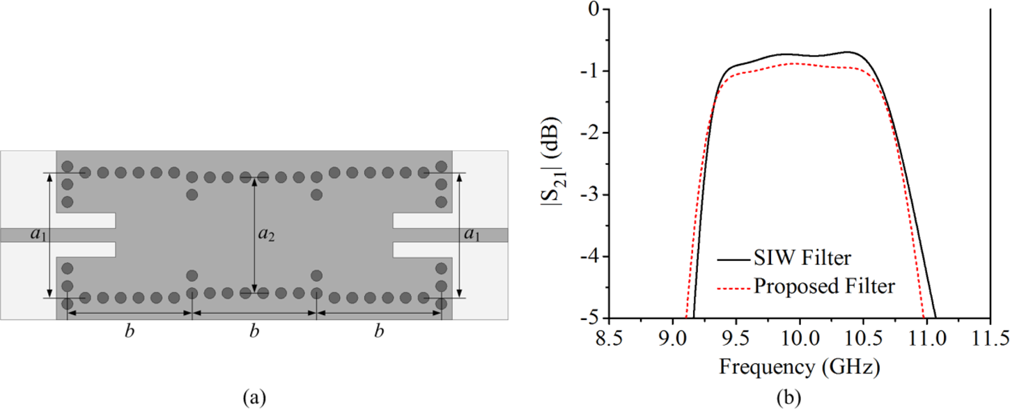
Fig. 10. (a) Structure of the conventional SIW third-order inline filter and (b) comparison of simulated |S 21| between conventional and proposed SIW filters.
Above results show that a compact third-order bandpass filter can be designed using two SIW cavities and a short-circuited coplanar line. The CF and the bandwidth of the filter can be controlled by adjusting the structural parameters of the filter. In addition, wide-stopband performance can be obtained by suppressing the passband constituted by the TE102 modes. The design steps of the filter can be summarized as follows:
(1) Determine the desired specifications of the filter such as the CF (f 0) and FBW (Δ).
(2) The initial values of the structural parameters a, b, and l are determined for desired f 0.
(3) The geometrical parameters g, l, and w 4 can be determined for appropriate f 1, f 2, and f 3 that satisfy the desired f 0 and Δ. It is suggested to choose a small value of g in order to suppress the passband created by TE102 mode.
(4) Next, the lf is adjusted to achieve better return loss in the passband. It should be noted that the CF and the bandwidth are slightly modified when lf is adjusted.
(5) Finally, the dimensions of the filter are fine tuned to obtain the desired filter specifications.
Fabrication and measurement
A compact third-order bandpass filter with wide-stopband performance is designed, fabricated, and measured to validate the proposed approach. The specifications of the filter are: CF of f 0 = 10 GHz and 3-dB FBW of Δ = 17.5%. The final dimensions of the filter are: a = 11.25, b = 11.2, wf = 1.2, lin = 1, lf = 6.51, t = 0.4, g = 2.85, l = 10.34, w 1 = 1.8, w 2 = 1.4, w 3 = 1, and w 4 = 0.2 (unit: mm). Figure 11(a) shows the photograph of the fabricated filter, and the simulation and measurement results are presented in Fig. 11(b). The measurement results show that the CF of the filter is f 0 = 9.97 GHz and the 3-dB FBW is Δ = 14.74%. The measured minimum in-band insertion loss is around 1.65 dB, and the passband return loss is higher than 10 dB. In addition, two TZs are observed at 15.25 and 18.74 GHz in the measured response of the filter. Moreover, the first higher-order mode TE102 is suppressed below −25 dB, and the rejection level is below −20 dB from 12.08 to 19.35 GHz (1.94f 0). The stopband rejection of the filter is limited due to the presence of the second resonant mode of the short-circuited coplanar line at around 19.64 GHz. Furthermore, the simulated radiation loss R r is extracted using the relation R r = 1 − |S 11|2 − |S 21|2 under the conditions of the lossless substrate and conductor. It can be observed that the radiation loss is below 5% in the frequency range of 6–19.6 GHz, as shown in Fig. 11(b), which implies that the proposed structure has very small radiation loss. The overall filter size excluding microstrip feedlines is 23.4 mm × 12.25 mm, which is equivalent to 1.47λ g × 0.77λ g, where λ g is the guided wavelength at f 0. Moreover, the simulation and measurement results are in close agreement. The discrepancies in the measurement results can be attributed to fabrication tolerances and losses caused by SubMiniature version A connectors.

Fig. 11. (a) Photograph of the fabricated filter and (b) simulated and measured results.
Figure 12 shows the simulated E-field distributions in the proposed filter at 10 GHz (f 0) and 16 GHz (f 102). It can be seen that TE101 mode in the cavities and the short-circuited coplanar line constitute the passband while the TE102 mode is successfully suppressed, and the passband due to TE102 mode is not generated. Moreover, Table 1 summarizes the comparison of the proposed filter with reported compact filters using SIW and planar resonators. As can be observed, the proposed filter meets given filter specifications, and shows the advantages of wide bandwidth and wide-stopband rejection while maintaining compact size.
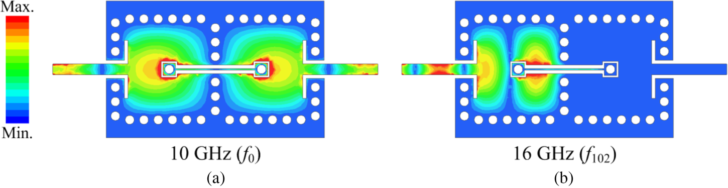
Fig. 12. Simulated E-field distributions in the proposed filter at (a) 10 GHz (f 0) and (b) 16 GHz (f 102).
Table 1. Comparison of the proposed filter with reported compact filters using SIW and planar resonators

f 0, center frequency; BW, bandwidth; IL, insertion loss.
a Estimated data.
Conclusion
This article presented a compact bandpass filter using two SIW cavities and a short-circuited coplanar line introduced between the cavities. The third-order filter response was obtained using TE101 modes of the cavity and the fundamental mode of the short-circuited coplanar line. The proposed approach provides significant size reduction in comparison with conventional SIW filters. In addition, wide-stopband performance has been obtained by suppressing the passband generated by the TE102 modes of the cavity. The presented filter shows the advantages of the planar structure, compact size, low loss, wide bandwidth, wide-stopband rejection, and ease of fabrication, which make it a suitable candidate for microwave applications.
 Amit Ranjan Azad received the B.Tech. degree in Electronics and Communication Engineering from West Bengal University of Technology, West Bengal, India, in 2010, the M.Tech. degree and Ph.D. degree in RF and Microwave Engineering from Indian Institute of Technology Kharagpur, West Bengal, India, in 2012 and 2019, respectively. Since 2019, he has been a faculty member with the Department of Electrical and Electronics Engineering at Birla Institute of Technology and Science Pilani, Hyderabad Campus, Telangana, India. His research interests include the synthesis, analysis, and design of high-performance microwave bandpass filters for modern wireless communication applications.
 Akhilesh Mohan received the B. Tech. degree in Electronics Engineering from Kamla Nehru Institute of Technology, Sultanpur, India, in 2002, the M.Tech. degree and Ph.D. degree in Microwave Engineering from Indian Institute of Technology Kanpur, Uttar Pradesh, India, in 2004 and 2009, respectively. From 2009 to 2010, he worked as a Scientist at Space Applications Center, Indian Space Research Organization, Ahmedabad, India. From 2010 to 2013, he was a faculty member with the Department of Electrical Engineering at Indian Institute of Technology Jodhpur, Rajasthan, India, where he was involved in teaching and research activities. Since 2013, he has been a faculty member with the Department of Electronics and Electrical Communication Engineering at Indian Institute of Technology Kharagpur, West Bengal, India. Dr. Mohan has authored or co-authored more than 110 peer reviewed international journals and conference papers. His research interests include the design of microwave filters and planar antennas for wireless communication systems.


