


I. INTRODUCTION
When the work of Pendry et al. [Reference Pendry, Schurig and Smith1] about transformation electromagnetics (TE) appeared in 2006, it drew the attention of many research groups all over the world. It was clearly a breakthrough, because this work claimed the possibility of manipulating and controlling electromagnetic waves as never before. The flexibility in electromagnetic design was achieved using metamaterials [Reference Schurig2] or composite materials, where the permittivity and permeability can be modified [Reference Tichit, Burokur, Germain and De Lustrac3]. The experimental application used to illustrate the theoretical principle was the invisibility cloak device. Despite of this first illustration, many issues about the device performance were highlighted such as narrow bandwidth, infinite phase velocities, or excessive dispersive losses [Reference Pendry, Schurig and Smith1]. These issues limit the performances of the invisibility cloaks made with this method [Reference Kwon and Werner4]. In this publication, a flat all dielectric TE-based reflector is theoretically described as in [Reference Kong, Wu, Kong, Huangfu, Xi and Chen5], then we introduce and highlight simplifications that make TE devices feasible and potentially useful, avoiding resonant structures as the ones used in [Reference Tichit, Burokur, Germain and De Lustrac3] or [Reference Kwon and Werner4]. In Section II, the principle of TE is reviewed. In Section III, the full description of a flat reflector design is presented, and the methodology to achieve different permittivity values with a single dielectric is described as well. Simplifications that lead to the use of an only Teflon structure with holes are also explained. The simulations results of different configurations for the flat reflector are presented in Section IV and finally conclusions are drawn.
II. PRINCIPLE OF TE
TE is a powerful theoretical tool, which enables the design of new devices in optics and microwaves as never before. TE is based on the principle of Fermat concerning the geometrical path of light. This principle gives the condition of a light trajectory in an inhomogeneous media. Usually, the light follows the shortest path between two points. In some particular cases, it could take the longest path as well. This optical path length S described in equation (1) is the Fermat's principle, where n is the refractive index and dl is the line element detailed in (2).
 $$S=\vint {n.dl}\comma \;$$
 $$dl=\sqrt {dx^2+dy^2+dz^2}.$$
The following methodology of TE design is widely applied in many applications like [Reference Tichit, Burokur, Germain and De Lustrac3, Reference Kwon and Werner4]. This method has two key points which are described by the following equations: the first one is the invariance of Maxwell's equations under any coordinate system (3), and the second one is the geometry-material dependence explained in (4).
 $$\eqalignno{&\nabla \times E = - j\omega \mu .H\comma \; \quad \nabla \times E^{\prime} =- j\omega \mu ^{\prime}H^{\prime}\comma \; \quad \cr &\nabla \times H = j\omega \varepsilon .E\comma \; \quad \nabla \times H^{\prime} = j\omega \varepsilon ^{\prime}E^{\prime}\comma \; &\lpar 3\rpar}$$
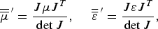 $$\overline{\overline \mu } ^{\,\prime} = \displaystyle{{J\mu J^T } \over {\det J}}\comma \; \quad \overline{\overline \varepsilon } ^{\,\prime} = \displaystyle{{J\varepsilon J^T } \over {\det J}}\comma \;$$
where J is the Jacobian, a mathematical tool that makes possible the transformation between two coordinate systems, i.e. for TE, between a real space where space is the transformed one, and a virtual space where the space remains itself. Equation (4) allows us to calculate the constitutive parameters profile (ε r and μ r) that will be used to build the final structure.
III. FLAT REFLECTOR
An interesting application of TE on antenna design is the reduction of the thickness of a parabolic reflector when replacing it with a flat structure. Usually parabolic reflectors allow achieving high directivity in antennas. In [Reference Kong, Wu, Kong, Huangfu, Xi and Chen5], the profile of a planar antenna is theoretically calculated using TE. Then, our paper aims to establish a simple methodology which leads to demonstrate that a flat structure is able to replace a parabolic reflector with improvements in terms of dimensions, performance, and simplicity in the realization. To design this device, the parabolic equation is used in this transformation to denote the mathematical link between the two spaces as in (5), where p is the focal distance, d and e are the thickness of the flat and parabolic reflector, respectively. We can notice in (5) that x is the only coordinate that changes. The values of d and e are 0.1 and 0.15 m, and it shows a reduction of the structure's thickness. The real space and virtual space are shown in Fig. 1. The virtual space is represented by the parabolic structure and the real desired space by the flat one. In Fig. 1(a), the cross-section of the flat structure is presented. The TE-based material is located between the source and the metallic boundaries. In Fig. 1(b), the cross-section in Cartesian coordinates of a metallic parabolic reflector is presented as well.
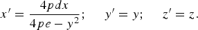 $$x^{\prime} = \displaystyle{{4pdx} \over {4pe - y^2 }}\semicolon \; \quad y^{\prime} = y\semicolon \; \quad z^{\prime} = z.$$
It is possible to calculate the constitutive parameters of the material needed to achieve the flat structure using equation (5) for the TE. This leads to a material profile expressed in two tensors: ε r and μ r. Consequently, some approximations are needed in order to reduce the number of components of the tensors, and thereby making the structure realizable. Therefore, we consider a polarization with E-field along the O z-axis. Then the three resulting non-zero components are μ xx, μ yy, and ε zz. The range of values for the permeability μ xx varies from 0 to 100, with a value near 1 in the central region around y = 0, for μ yy from 0.2 to 1.1, with also a value near 1 in the central region, and for permittivity ε zz from 0.2 to 1.45 as is seen in Figs 1(c)–1(e). Usually, these values can only be achieved using metamaterials, which lead to a complex realization.

Fig. 1. Cross-section of reflectors: (a) TE-based flat structure, PEC boundaries in blue. (b) Parabolic reflector. TE structure profile where: e = 0.15 m, d = 0.1 m, and p = 0.15 m; (c) μ xx; (d) μ yy; and (e) ε zz.
Two-dimensional (2D) simulations at 5 GHz of the reflectors were performed with Comsol Multiphysics. A rectangular port in transverse electric mode (i.e. polarized along the z-axis) as source, is located at the focal point. The simulated distributions of the normalized magnitude of the z-component of the electric field E of three structures, the classical parabolic reflector, the flat rectangular reflector with metallic boundaries and a perfect electric conductor (PEC) plane reflector are presented in Fig. 2.
Fig. 2. Normalized |E z| distribution at 5 GHz: (a) parabolic reflector, (b) flat reflector, and (c) PEC reflector.
The electric field distributions are quite similar for the two first reflectors. However, the flat reflector presents more directivity than the parabolic one because the radiation is more concentrated toward the propagation direction. This can be explained as a result of simplifications on tensors made in the design process. The field distribution for the only PEC reflector is not useful as expected.
In this work, the use of only standard dielectric materials is needed in order to simplify the realization. In this way, additional approximations are also applied to set a constant value of permeability (μ r = 1) and to have a structure only defined by a variable permittivity [Reference Tang, Argyropoulos, Kallos, Song and Hao6]. This approximation is justified as the value of μ r is near 1 in the central region of the structure, where the field is concentrated. The next step is the discretization of the material in 32 dielectric blocks (concentric rings) as shown in Fig. 3. The discretized values of permittivity are taken from the profile of ε zz in Fig. 1(e). Relative permittivity values range from 0.2 to 1.45. It is noticed that some values are below 1 (dispersive values), which does not correspond to standard materials. Therefore, the case where dispersive values are replaced by a relative permittivity of one is analyzed in the following paragraphs. As the values of permittivity below 1 occur only at the edges of the structure where the field is weak, this approximation is also justified.
Fig. 3. TE structure profile with discretized values of permittivity.
Then, the profile in Fig. 3 is rotated around the x-axis to obtain a three-dimensional flat reflector. As a result, the flat reflector is a cylindrical structure of 60 cm diameter with different annular regions. Furthermore, the realization of the structure is possible using a drilling technique, which involves drilling holes in standard materials to achieve a variable permittivity structure. The density of holes determines the value of the relative permittivity as established in [Reference Schulwitz and Mortazawi7]. This density is varied by changing the angular distance d a between holes and keeping the radial distance d r constant (see Fig. 4). The diameter of the holes is 4 mm, which represents 0.067λ at 5 GHz. Equation (6) allows us to calculate the different values of the synthesized permittivity from ε d to ε a, the permittivity of the Teflon and the air, respectively.
 $$\varepsilon _{synth} = \varepsilon _d f_d+\varepsilon _a f_a = \varepsilon _d - \lpar \varepsilon _d - \varepsilon _a \rpar f_a .$$
The factor f d represents a volume ratio of the dielectric and f a represents the volume ratio of the air inside the layer. In this case, only air fills the holes, but they can be filled with other dielectrics to achieve other ranges of permittivity values. To build up the final prototype of the reflector, the only dielectric used is Teflon, which has a permittivity of 2.2. Then, the range of relative permittivity values (0.2–1.45) is shifted to (1.6–2.2). As shown in Fig. 4, only one layer of Teflon with holes is used to construct the different regions.
Fig. 4. (a) Front view of dielectric structure. (b) Front view in details: d a angular distance and d r radial distance between holes.
IV. RESULTS
Radiation patterns in copolarization obtained with CST Microwave Studio (Transient solver) at 5 GHz are shown in Fig. 5. As a source, a small horn antenna linearly polarized along the z-axis is located at the focal point. A comparison between the results obtained with structure with dispersive parameters and the other one with non-dispersive parameters is presented in order to see how the dispersive values affect the performances. A slightly better performance in terms of gain and half-power beamwidth (HPBW) of the dispersive structure is shown, whereas the non-dispersive structure presents some degradation like higher levels of side lobes. However, the performance is quite acceptable.
Fig. 5. (a) Comparison of radiation patterns between three reflectors at 5 GHz. (b) Comparison of HPBW of dispersive and non-dispersive reflectors at 5 GHz.
The gain obtained with the PEC surface as reflector is low as expected. In terms of maximum gain, the dispersive structure's one is 9.4 dB, which is 5 dB greater than the PEC reflector's one. The non-dispersive structure presents a maximal gain of 9.8 dB, which is higher than the dispersive reflector, because of higher values of permittivity used in the non-dispersive structure.
Then, HPBW is presented in Fig. 5(b). The HPBW of the dispersive structure is 20°, which is larger than the non-dispersive one (16°). Only θ = 90° planes (XY-plane) are presented in order to present the same plane as the 2D case presented in Fig. 2 and because of the polarization along the z-axis.
In Fig. 6, the radiation pattern of the structure with holes is shown, in order to be compared with the dispersive and non-dispersive structures presented before. The Teflon reflector is positioned 5 mm from the horn antenna in order to minimize the oscillations in the radiation pattern, which occur when the reflector is in contact with the horn antenna. Results are relatively close, the HPBW are 20°, 16°, and 21° for the dispersive, non-dispersive structure and the drilled structure, respectively. The maximal realized gain in the broadside direction is 12.2 dB for the drilled reflector, which is higher than the one of the other reflectors. This can be explained by the fact that the values of permittivity are higher than in the other cases. The back lobe level is higher in the case of the Teflon with holes (−6.8 dB) than in other cases (>−10 dB). The variation can be caused by the separation of 5 mm between the horn antenna and the drilled dielectric. Finally, the behavior of the drilled reflector versus frequency has been studied in the operating bandwidth of horn antenna. The radiation pattern at 4.8 and 5 GHz is presented in Fig. 6(b). It can be seen that both radiation patterns are relatively similar in terms of gain and HPBW.
Fig. 6. (a) Radiation patterns comparison between the dispersive and non-dispersive reflectors and the drilled one at 5 GHz. (b) Teflon reflector radiation patterns at 4.8 and 5 GHz.
V. CONCLUSION
In this paper, we have proposed a method to design a flat reflector in order to reduce the thickness of the structure, based on TE principle and using dielectric materials only. Choosing carefully the approximations and simplifications to be made in the different components of the permeability and the permittivity tensors of the material is important in order to achieve a feasible structure. A comparison between dispersive and non-dispersive flat reflector has demonstrated that this last one has better performances in terms of gain and HPBW. As the frequency is not taken into account in the profile calculation, this method can be used at other frequencies. Furthermore, we have demonstrated that different values of permittivity can be achieved by varying the density of holes in the different regions of the structure. This low-cost method could be very useful to realize structures with varying permittivity. Finally, the last results obtained with drilled reflector are better than the previous configurations in terms of gain and HPBW.
ACKNOWLEDGEMENT
The research leading to these results has received funding by British and French Ministries of Defence (DSTL and DGA), through the European Defence Agency (EDA) contract MIMiCRA (Metamaterial Inspired Microwave Conformal Radar Antennas).
 Mark Clemente Arenas was born in Cusco, Peru. In 2005, he received his bachelor degree in Electronics Engineering at Universidad Nacional de San Antonio Abad del Cusco, in Peru. In 2011, he received his master degree in engineering from PolyTech Marseille. He also received a Master of Sciences degree in RF Communicating Objects from the Université de Provence in France. In 2011, he joined Orange Labs in Nice as intern where he worked in channel modelization for MIMO Antennas. In September 2011, he joined Telecom ParisTech as a Ph.D. student where he works on applications of Transformation Electromagnetics in antenna design. His areas of interest are mobile communications, antenna design, etc.
Anne Claire Lepage received an M.S. degree in Fundamental Physics in 1999 from Henri Poincaré University, Nancy, France and an M.S. degree in Electronics and Telecommunications in 2001 from Pierre and Marie Curie University, Paris. She received her Ph.D. degree from Telecom ParisTech, Paris, in 2005. She joined the Radiofrequency and Microwave Group of Telecom ParisTech as Associate Professor in 2007. Her research activities encompass compact wideband bipolarized antennas and metamaterials for wideband low profile antennas and are related to various applications fields such as cognitive radio, LTE, airborne, and space systems.
 Xavier Begaud received an M.S. degree in Optics, Optoelectronics, and Microwaves, from Institut National Polytechnique de Grenoble (INPG) in 1992. He received his Ph.D. degree from the University of Rennes in 1996 and the habitation degree from Pierre and Marie Curie University (Paris 6) in 2007. He joined the Télécom ParisTech (formerly Ecole Nationale des Telecommunications) in 1998, where currently he is the Professor and Head of the RF & Microwave group (RFM) at COMmunications and ELECtronics Department (COMELEC). His research topics include theory, conception, modeling, and characterization of wideband, bipolarized and 3D antennas with special emphasis on numerical methods. Currently, his research activities include design of metamaterials, channel sounding, and mutual coupling analysis in the framework of ultra-wideband and software radio. He has published over 160 journal papers, patents, book chapters, and conference articles. He has organized two international conferences as the general chairman and edited one book.
Paul-Henri Tichit received his Master degree in theoretical Physics in 2007. In 2012, he received the Ph.D. degree from the Institut d'Electronique Fondamentale (IEF) – University of Paris Sud, France. His Ph.D. research works dealt with the technique of transformations optics and the application of this methodology to design new electromagnetic devices such as invisibility cloaks, taper, and novel antennas, through the use of metamaterials. He is actually pursuing his research on source transformations as a post-doctoral fellow at the IEF and is involved in miniaturization of devices and sources teleportation.
André de Lustrac received the Ph.D. degree in Electrical Engineering in the microwave domain from the Institut d'Electronique Fondamentale (University of Paris Sud) on Josephson logic devices in 1986. From 1989 to 1992 he was an Assistant Professor at the Institute of Technology of Cachan, France. He is currently full professor at the University of Paris 10, France. From 2002 to 2007 he was the head of the SITEC department of the University of Paris 10 (Industrial Systems and Communication Techniques). He has published more than 160 papers in journals and international conferences in the areas of the simulation and applications of the Josephson junctions in digital circuits, the simulation methods of high-frequency III–V transistors (HEMT) and quantum circuits, and last but not least, on photonic band gap materials and metamaterials in the microwave and optical domains. With his research team at the Institut d'Electronique Fondamentale, he explores the physics and the future industrial applications of these materials in telecoms and aeronautics. From 2006 to 2012 he was the scientific adviser for the nanotechnology domain for the French Ministry of Research and Higher Education. He is now the head of the Institut d'Electronique Fondamentale of the University of Paris Sud.

