


Introduction
Fast, accurate, and reliable impedance matching of high-power manufacturing processes in the lower industrial, scientific, and medical (ISM) frequency bands such as dry etching, laser welding, and RF heating has gained increasing interest in the past years due to the higher integration level in our modern communication, computer, automotive, and consumer electronics [Reference Goodyear and Cooke1–Reference Sherpa, Ventzek and Ranjan3]. Especially at 13.56 MHz, these manufacturing processes generate a demand for low-loss, fast, and highly tunable RF varactors [Reference Ranjan, Sherpa, Engelmann and Wise4]. In this work, varactors based on fully-printed, ferroelectric barium strontium titanate (BST) are presented. BST as a tunable dielectric in varactors has been under investigation for several years now and shows promising results regarding Q-factor, tunability, tuning speed, and power handling capabilities. In comparison to state-of-the-art technologies, such as mechanically tuned vacuum capacitors or switchable capacitor banks, utilizing high-power pin diodes, BST-based varactors offer a significantly higher tuning speed and continuous tuning [Reference Preis, Wiens, Kienemund, Kendig, Maune, Jakoby, Heinrich and Bengtsson5,Reference Kienemund, Fink, Abrecht, Bigler, Binder, Jakoby and Maune6]. A disadvantage of BST-based varactors is the bias induced piezoelectricity in the ferroelectric layer, introducing a dipole moment. A superimposed RF voltage latches onto the induced dipole moment, resulting in mechanical/acoustical vibrations, which reduce the varactors Q-factor and therefore its power-handling capabilities [Reference Gevorgian, Vorobiev and Lewin7,Reference Tappe, Böttger and Waser8]. In this paper, a fully-printed thick film varactor is demonstrated in a matching circuit and input power levels of up to 1 kW, with an implemented interference-based acoustic suppression technique, described and verified in [Reference Kienemund, Walk, Bohn, Binder, Jakoby and Maune9]. The suppression mechanism utilizes novel fully-printed doublemetal–insulator–metal (MIM) varactor cells. The performance of the varactor is compared to an acoustically non-optimized varactor design presented in [Reference Kienemund, Fink, Abrecht, Bigler, Binder, Jakoby and Maune6]. To the authors best knowledge, this is the first time a fully-printed double MIM varactor based on BST is demonstrated under high-power conditions. In section “Acoustic design of the varactor” the acoustical suppression technique is presented in the newly designed varactor utilizing a double MIM structure with an acoustical simulation. The approach is implemented in a new high-power optimized varactor design and characterized under small and large signal conditions in section “Implementation of a high-power optimized varactor based on double MIM structures”. The results are discussed and concluded in section “Conclusion”.
Acoustic design of the varactor
The presented acoustic suppression technique is based on the work of [Reference Lakin, Kline and McCarron10,Reference Zheng11] and presented in detail in [Reference Kienemund, Walk, Bohn, Binder, Jakoby and Maune9]. As a fundamental structure for the theory, a layered double MIM setup is assumed, see Fig. 1. The model features an infinitesimal thin electrode in between the two ferroelectric layers and infinitely thick top and bottom electrodes. Based on the model and the complete constitutive equation for the piezoelectric effect with electrostriction [Reference Newnham12,Reference Zheng13]:
 $$ u = s \sigma + dE + aE^2 $$
calculating the mechanical strain u of the material, the suppression technique is derived. Input parameters are the mechanical stress σ linked to the strain by the elastic compliance s, the electric field E linked with the piezoelectric coupling factor d, and the square of the electric field colligated with the electrostrictive coefficient a. It is important to note, that all of these quantities are dependent on their spatial orientation. Here, the directivity is simplified to a single direction according to Fig. 1. As BST has several distinctive lattice grid arrangements, which are temperature dependent and determine whether or not the material experiences piezoelectricity, it is important to derive the equation for the correct lattice grid arrangement and therefore temperature. In this work, BST with a stoichiometric ratio of barium to strontium of 60–40% is processed, resulting in a Curie temperature of 0°C. As the material is not supposed to be operated below 20°C in the intended application, the material is in the paraelectric phase experiencing no piezoelectricity, due to its centrosymmetric lattice grid arrangement [Reference Kohler, Nikfalazar, Friederich, Wiens, Sazegar, Jakoby and Binder14]. To derive the equation for the paraelectric phase, the material is now assumed with no piezoelectricity d = 0 and no stress applied to it (σ = 0) as it is not mechanically loaded in any way. Furthermore, a superimposed electric field with the static DC component  $ {\hat E}_{DC}$ and the alternating RF component
 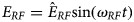 $E_{RF}= {\hat E}_{RF} {\sin}(\omega _{RF} t)$ is applied to the material. The mechanic strain u can be written with equation 1 [Reference Oshiki and Fukada15]:
 $$ \eqalign{u & = a ({\hat E}_{DC}+E_{RF})^2 \cr & = a{\hat E}_{DC}^2+2aE_{RF}{\hat E}_{DC}+aE_{RF}^2 \cr & =\underbrace{a({\hat E}_{DC}^2 + {\displaystyle{1} \over {2}}{\hat E}_{RF}^2)}_{\rm static} \cr & + \underbrace{2a {\hat E}_{DC}{\hat E}_{RF}{\sin}(\omega_{RF}t)}_{\rm piezoelectric} \cr & -\underbrace{{\displaystyle{1} \over {2}}a {\hat E}^2_{RF}{\sin}(2\omega_{RF}t + {\displaystyle{\pi} \over {2}})}_{\rm electrostrictive}} $$
In equation 2, three major terms can be identified, having impact on the mechanical strain of the material:
• A static term, which is not exclusively dependent on the DC component of the external electrical field. In most applications however, E DC is chosen much larger than E RF (factor of 10).
• A term, that is linearly dependent on the alternating component of the external electric field. This term describes a reoccurring piezoelectric effect in the material, even though it does not exhibit piezoelectricity in the paraelectric phase. The apparent piezoelectric coupling factor is called
 $e=2a {\hat E}_{DC}$. In contrast to the piezoelectric coupling factor d, e is not constant but increasing with the DC component of the external electric field [Reference Oshiki and Fukada15]. Usually, the electrostrictive coupling factor a is much smaller than the piezoelectric coupling factor d [Reference Li, Jin, Xu and Zhang16]. Due to the amplification of a with E DC however, the apparent piezoelectric coupling factor e is in the range of d [Reference Oshiki and Fukada15]. Descriptively, the amplification of a can be described as a distortion of the cubic lattice up to the degree it becomes tetragonal and therefore ferroelectric again [Reference Gevorgian17].
• A second-order term, representing the electrostrictive component of the induced mechanic strain. The frequency of this strain component is twice the excitation frequency.


Fig. 1. Double MIM fundamental model.
The suppression technique utilizes the tunable apparent piezoelectric coupling factor e by applying an antipolar electric DC field in the two BST layers, resulting in an antipolar apparent piezoelectric coupling factor e and − e in the adjacent BST layers. Thereby, an excited acoustic wave is unable to couple to adjacent layers, resulting in significantly reduced losses. However, the technique is only applicable when both BST layers behave exactly the same. Otherwise an excited acoustic wave does not interfere destructively with its 180° inverted counterpart. The design is implemented in a piezoelectric/acoustic simulation in COMSOL to depict the mechanic displacement pattern in the structure at 13.56 MHz with and without correctly applied biasing voltage, resulting in operational and disabled acoustic suppression in the structure. For this, the cell with the given dimensions and layer thicknesses depicted in Fig. 2 is modeled in COMSOL. As the described electrostrictive effect is not simulatable, it is mimicked by anti polarizing the piezoelectric coupling factor of the material in both layers. First, the piezoelectric coupling of the material is limited to the vertical direction (z-direction) of the structure, as it represents the direction for the dominant longitudinal pressure mode. As a result, all transversal modes, which may be excited parasitically, are not considered in the simulation.
 $$ \eqalign{& d = \left[ \matrix {d_{xxx} & d_{xyy} & d_{xzz} & d_{xyz} & d_{xxz} & d_{xxy} \cr d_{yxx} & d_{yyy} & d_{yzz} & d_{yyz} & d_{yxz} & d_{yxy} \cr d_{zxx} & d_{zyy} & d_{zzz} & d_{zyz} & d_{zxz} & d_{zxy}} \right] \cr d_{33} & = e_{33}= \left[ \matrix {0 & 0 & 0 & 0 & 0 & 0 \cr 0 & 0 & 0 & 0 & 0 & 0 \cr 0 & 0 & d_{zzz} & 0 & 0 & 0}\right]} $$
Fig. 2. 3D and cut plane view of the varactor design as well as the SEM cross-sectional image of the processed double MIM structure. The intended layer thickness is achieved by the applied screen-printing process accurately. (a) Cut through a double MIM varactor cell with dimensions. (b) SEM cross-sectional image of the double MIM cell.
The antipolarized coupling factor, which is introduced during characterization by a DC biasing voltage applied to the middle electrode, is mimicked by inversing the piezoelectric coupling factor in z direction of the simulation in one of the layers. For the case with disabled acoustic suppression, an identical piezoelectric coupling factor is applied to both layers, mimicking a DC biasing voltage from bottom to top electrode or vice versa.
 $$ \eqalign{{\rm Layer1} & = d_{33} \cr {\rm Layer2} & = -d_{33}\; { (\hbox{active suppression})} \cr {\rm Layer2} & = d_{33}\; {(\hbox{inactive suppression})}} $$
The obtained mechanical displacement pattern in z-direction at 13.56 MHz in the double MIM structure, the electrodes as well as the substrate for the inactive and active suppression case are depicted in Fig. 3.

Fig. 3. Comparison between a double MIM varactor cell with and without correctly applied DC biasing potential at the middle electrode to provide for acoustic interference suppression. The displacement pattern in the active suppression case is given with a different scaling to show how it changes within the double MIM structure compared to the inactive case. (a) Acoustic suppression disabled (top) and enabled (bottom). (b) Acoustic suppression enabled with different scaling.
For the inactive suppression case, a strong mechanical displacement pattern is obtained, especially in the double MIM structure itself and below the substrate. The acoustic wave is prone to couple to adjacent layers beneath the substrate and surrounding air at the top electrode. For the case with enable acoustic suppression and the same scaling in the center picture of Fig. 3, barely any acoustic activity is visible, indicating a strong suppression. Therefore, a different scaling is applied in the bottom picture. A distorted displacement pattern from the inactive suppression case is obtained, with strong acoustic activity on the middle electrode in z-direction. The pattern indicates, that the middle electrode is vibrating in z-direction, absorbing the acoustic wave. From intuition, this is what one would expect when the mechanic strain u is introduced antipolarized in the layers. One expands, one contracts with just little displacement at the boundaries to adjacent layers. Overall the simulation verifies the implemented acoustic suppression technique in the designed high-power varactor cell.
Implementation of a high-power optimized varactor based on double MIMstructures
For the first time, a fully-printed, double MIM-based varactor capable of operating at power levels up to 1 kW is developed. The varactor is based on an interconnectable capacitive matrix consisting of double MIM varactor cells. The connection between cells is made after small signal characterization to form a macroscopic varactor. A highly conductive silver paste from Chemtronics is used for this, applied with a stencil. Thereby, a widely homogeneous depositioning pattern is achieved. In regard to the design process, main focus is laid upon increased creepage distances, higher electrical strength and durability of the varactor by increasing tolerances and layer thicknesses in comparison to the design process presented in [Reference Kienemund, Walk, Bohn, Binder, Jakoby and Maune9].
Varactor design
The high-power varactor consists of several double MIM varactor cells interconnectable in a capacitive matrix. The main reason for this distributed design is the possible exclusion of damaged cells from the matrix. Each cell features an electrode overlap area of 1.1 mm × 5.5 mm, resulting in a theoretical cell capacity of 300 pF with εr = 230 and a layer thickness of 20 µm. The difference of the high-power optimized design compared to the cells presented in [Reference Kienemund, Walk, Bohn, Binder, Jakoby and Maune9] are the increased size of each cell to obtain a reasonable overall capacitance value of the structure and increased tolerances from 50 to 250 µm. of each layer to increase creepage. The varactor in a perspective view is depicted in Fig. 4.

Fig. 4. Perspective view on the capacitive matrix of the high-power varactor.
Varactor processing
Cu-F co-doped Ba0.6Sr0.4TiO3 is prepared in a modified sol–gel process [Reference Kohler, Nikfalazar, Friederich, Wiens, Sazegar, Jakoby and Binder14,Reference Zhou, Geßwein, Sazegar, Giere, Paul, Jakoby, Binder and Haußelt18]. The single MIM varactor is processed in three steps. In a first step, the bottom RF electrode is screen printed on an alumina substrate. For the electrodes the conductor paste C 1076 SD (LPA 609-022) from Heraeus is chosen. It is a solderable Ag/Pt conductor paste suitable for temperatures up to 850°C. In a second step, two layers of BST thick film are screen printed on the bottom electrode and dried at 80°C. A total BST layer thickness of 20 µm. is obtained. Subsequently, the middle electrode and two more layers of BST are printed and dried at 80°C. Eventually, the top electrode is printed and the whole structure is sintered at 850°C for 10 min. Considering the manufacturing process presented in [Reference Kienemund, Walk, Bohn, Binder, Jakoby and Maune9] and its effects on the suppression of acoustic resonances based on interference, the homogeneously processed case is applied to all four BST layers, resulting in equal material properties in the top and bottom BST layers. A SEM cross-sectional image of the homogeneously co-sintered double MIM structure is depicted in Fig. 2.
Small signal characterization
The varactors are characterized with a 1-Port measurement from 10 to 25 MHz with a Keysight E4991B impedance analyzer connected to a Cascade Summit 12K wafer prober with a 1250 µm ground-signal (GS) probe. A biasing voltage range from 0 to 200 V is used for characterizing the varactors. A protective Bias-Tee PSPL5531 is connected to the impedance analyzer port in case of an electrical breakdown of a cell during characterization. With a 100 kΩ resistive needle the middle electrode of each cell is connected and the biasing voltage is applied. The equivalent circuit diagram of the biasing concept is depicted in Fig. 5.

Fig. 5. Varactor cell small signal characterization scheme and equivalent circuit model. (a) Cut through a double MIM varactor cell and connected biasing scheme. (b) Equivalent circuit.
The varactor cell small signal characterization results in regard to capacitance and Q-factor defined as  $Q=\Im {\{\underline {Z}\}}/\Re {\{\underline {Z}\}}=1/\omega RC$ in unbiased and biased state are depicted in Fig. 6. The tunability is defined as:
 $$ \tau = {\displaystyle{C(0V)-C(V_{bias})} \over {C(0V)}} $$
Fig. 6. Capacitance and quality factor of one double MIM cell of the high-power varactor.
The varactor cells show a tunability of 34% reducing the capacitance from 350 pF in unbiased state to 232 pF in biased state at 13.56 MHz. A resonance-free Q-factor spectrum is measured with an increased Q-factor of 151 in biased state from 107 in agreement with the results of [Reference Kienemund, Walk, Bohn, Binder, Jakoby and Maune9].
Large signal characterization
The power measurements are carried out in a 50 Ω setup with two L-match circuits in back-to-back configuration and a 50 Ω high-power load provided by COMET. The equivalent circuit model of the setup is depicted in Fig. 7.

Fig. 7. Equivalent circuit diagram of the large signal characterization setup.
To characterize the varactor, first a load condition  $Z^{\ast}{M}$ for the measurement has to be set up. The load impedance is composed of the 50 Ω high-power load and a preceding L-match circuit, in Fig. 7 termed as “Tunable Load”, tuning the load to an inductive plasma like impedance. Inductive plasma impedances are determined by their low real part and positive imaginary part. For the matching circuit including the DUT, low absolute values of the load impedance introduce more stressful electrical conditions. The load condition is left unchanged during the measurement. The characterization itself is performed in the “L-Match” denoted part of the system, see Fig. 7. The DUT varactor is installed in series connection to a tunable vacuum capacitor C Vac1 with a tuning range of 0.15 to 1.5 nF. The tuning position of C Vac1 is accessible by the system and controlled by a steepest decent algorithm to automatically match the load impedance to the 50 Ω of the generator. A phase/mag detector is installed for this purpose at the input of the “L-Match” denoted circuit. As the load condition connected to the system is kept constant, a capacitance change of the DUT by applying biasing voltage to it, results in a mismatch between load and generator, which is automatically compensated by C Vac1. By knowing the required overall capacitance C req = (1/C Vac1 + 1/C DUT)−1 in the shunt branch of the characterization L-match for the matched condition, the DUT capacitance can be extracted from the position of C Vac1. The Q-factor is extracted from a power loss measurement with the DUT installed and its reference without the DUT. C Vac2 is a tunable vacuum capacitor as well, with a tuning range of 50–500 pF and L an air cored inductor. C Vac2 and L are required to enlarge the matchable load impedance range but have no direct influence on the capacitance acquisition of the DUT capacitor during large signal characterization. A drawback of the measurement principle is the limited DUT capacitance range, that can be compensated by C Vac1, as a series stack of capacitances is dominated by the smallest partial capacitance value. For a DUT capacitance smaller than C req, C Vac1 is unable to compensate for and reinstate matching. Then, a different load condition has to be set up, resulting in altered electrical conditions of all components including the DUT. As aforementioned, a changed load impedance may result in a less stressful electrical state of the DUT varactor, meaning lower voltage, current, and dissipated power occur. As a result, for large signal characterization not only the input power is of interest but the exact voltage and current stresses applied to the DUT varactor, as well as its temperature. To obtain these data, the measurement setup monitors the input power from the generator and the output power of the back-to-back matching system to the 50 Ω load. The monitoring system consists of two Bird Model 4027A10M power sensors connected to Bird Model 4421 RF power meters 4421 provided by COMET. Due to the high RF power, a voltage or current monitoring system can not be installed. However, the voltages and currents are extracted from an exact model of the L-match circuit, which is valid as only highly linear vacuum-based capacitors and air cored inductors are installed in the circuit apart from the DUT. The printed varactor is soldered to an FR4 PCB holding the RF and DC biasing connectors as well as resistive biasing network. The mounted varactor module is depicted in Fig. 8. The RF/DC decoupling network consists of 100 kΩ resistors. Due to the expected high voltages and currents, the resistors are designed for a dissipated power of up to 2 W. For the macroscopic varactor, 16 by 4 cells are connected in parallel and series connection, respectively. A theoretical overall capacitance of 1.2 nF can be achieved with this setup. In general, a design aiming at a larger overall capacitance value is favorable as it can be adjusted to lower values later on by interconnecting less cells with each other. The mounted varactor module with a heat sink applied to the back of the varactor substrate is depicted in Fig. 8. The DC bias is applied via a coaxial plug.

Fig. 8. Front and backside of the assembled high-power varactor module with applied heat sink on the back of the varactor substrate. (a) Back side. (b) Front side.
The large signal measurement results are depicted in Fig. 9 in regard to capacitance, Q-factor, dissipated power, and temperature for zero-bias and biased state. For characterization two different load conditions are taken. The first load condition of 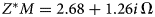 $Z^{\ast}{M} = {2.68+1.26i}\,{\Omega }$ is taken in accordance to [Reference Kienemund, Bohn, Fink, Abrecht, Bigler, Binder, Jakoby and Maune19] for power levels from 300 up to 500 W and creates a stressful loading state of the DUT varactor visible in the dissipated power trace of Fig. 9. At 500 W of input power, the dissipated power of the varactor as well as the temperature increases from 13.5 W and 35°C to 19.5 W and 42°C respectively. The tunability of the varactor decreases from 34.4% at 300 W of input power to 19.3% as the Q-factor increases from 34.8 at 300 W to 55.8. The varactor capacitance is thermally reduced by 28% from 2.5 to 1.8 nF. At this power level, an RMS voltage and current of 85 V and 13 A are applied to the DUT varactor. A conditioning effect is observed as the biasing voltage of 200 V is applied to the varactor. The effect is explained in more detail in section “Introduction”. During conditioning, the tunability of the varactor erratically increases to 30%, as the isolation of the BST layer increases, resulting in a DUT capacitance value outside of the measurement range of the circuit and an increase in Q-factor from 55.8 to 67. To readjust the measurement range, a load impedance of
 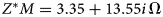 $Z^{\ast}{M} = 3.35 + 13.55i\,{\Omega }$ is set, creating a less stressful loading of the varactor. At 500 W of input power and the new loading state, an RMS voltage and current of 67 V and 10 A are applied to the DUT varactor, resulting in significantly reduced dissipated power and temperature, see Fig. 9. With this load at an input power level of 1 kW, the varactor achieves a tunability of 18.2% with a maximum dissipated power of 14.2 W and a maximum Q-factor of 142 for the whole varactor module with biasing network. The capacitance of the varactor is thermally decreased by 47% from 2.5 to 1.3 nF. The varactor withstands an RMS voltage and current of 140 V and 14 A with a maximum temperature of 50.2°C. Compared to the varactor presented in [Reference Kienemund, Fink, Abrecht, Bigler, Binder, Jakoby and Maune6], the results show a decrease in losses of 62%, a decrease in temperature of 33% while the product of RMS voltage and current for the here presented varactor is just slightly decreased by 5% from 2057 W of the varactor in [Reference Kienemund, Fink, Abrecht, Bigler, Binder, Jakoby and Maune6] to 1960 W.

Fig. 9. Large signal characterization results of the high-power varactor module for different input power levels and biasing states. (a) Capacitance and Q-factor of the high-power varactor for different input power levels in unbiased and biased state. (b) Dissipated power and temperature of the high-power varactor for different input power levels in unbiased and biased state.
RF conditioning
A major issue identified within the scope of this work is the vaporization of organic solvents in the printed BST layer during the sintering process. As a result, holes and craters arise on the BST layer surface. After printing the top electrode on the dielectric layer, channels between the electrodes arise, which significantly increase the conductivity of the BST layer, sometimes up to a complete short circuit. During large signal characterization with high RF power levels however, a conditioning effect is observed. A varactor with low tunability, due to a conductive channel in the dielectric layer creating a voltage divider with the resistive biasing network, gains tunability while being stressed with RF. The varactor is fully functional afterwards with increased tunability. In general, high voltage conditioning is a well-known technique to ensure proper discharge free high-voltage vacuum devices [Reference Fink, Gentsch, Heil, Humpert and Schnettler20,Reference Yang, Geng, Liu, Zai and Wang21]. Known techniques include DC, AC, and high-frequency-based conditioning [Reference Fink, Gentsch, Heil, Humpert and Schnettler20,Reference Faircloth22,Reference Budde and Kurrat23]. A key aspect during the conditioning process is the power brought into the discharge and how long it is applied [Reference Faircloth22]. High-power levels vaporize the metal irregularities more violent and tend to produce new ones [Reference Faircloth22]. Short high-power bursts melt the sharpest parts of an irregularity, creating a more homogeneous surface [Reference Faircloth22,Reference Küchler24]. RF conditioning at 13.56 MHz introduces periodic high-power levels in the ns region. Partial discharges take place in the same time realm, meaning no continuous arc is created [Reference Okubo, Hayakawa and Matsushita25] and the power intake into the irregularity is limited. It is assumed, that a gentle conditioning occurs in the thick film varactors, resulting in a gradual regression of the conductive channel until an isolating state is reached. Then, the voltage divider created by the MIM structure and the resistive biasing network is heavily in favor of the MIM structure, resulting in a significant increase in biasing voltage at the MIM structure and therefore tunability.
Conclusion
In this work, a fully-printed double MIM varactor structure is presented under high-power conditions, utilizing an acoustic resonance suppression technique presented in [Reference Kienemund, Walk, Bohn, Binder, Jakoby and Maune9] to reduce its losses. The theoretical background of the approach is described in detail and verified with an acoustic/piezoelectric simulation on an implemented high-power optimized double MIM varactor cell. It is shown, that the suppression principle works by entrapping the acoustic wave in the BST layers and the middle electrode, preventing it from coupling to adjacent material layers. Thereby, the acoustically radiated energy is minimized. A varactor optimized for high-power operation is implemented utilizing the studied acoustic suppression approach. The varactor, based on an interconnectable capacitive matrix with individually characterized varactor cells, shows a resonance-free spectrum from 10 to 25 MHz. After conditioning of the varactor, a tunability of maximum 32% at 600 W of input power is measured. At high-power operation up to 1 kW, the varactor shows significantly reduced losses of 64% compared to a prior presented design. The varactor remains tunable with 18.2% and a Q-factor of maximum 142.
Acknowledgments
The authors would like to thank S. Schober for the sample preparation and processing.
 Daniel Kienemund received his diploma in Electrical Engineering from RWTH Aachen University in 2013. Currently he is working towards a Ph.D. in the field of tunable components for high-power radio frequency matching circuits at the Institute for Microwave Engineering and Photonics of Technische Universität Darmstadt.
 Nicole Bohn received her diploma in dental technology from Osnabrück University of Applied Sciences in 2009. Since then she is working at the Institute for Applied Materials – Ceramic Materials and Technologies of Karlsruhe Institute of Technology. Her current responsibilities include the development, fabrication, and processing of tunable dielectric materials for microwave applications as well as the microstructural characterization of the specimen.
 Thomas Fink graduated with a diploma degree in Physics from Ludwig-Maximilians University in Munich in 1987, and he received a Ph.D. from Freie Universität Berlin in 1990. Subsequent affiliations include positions as research scientist at Columbia University (NY) and at Fraunhofer IAF (D) and as process engineer with ABB Semiconductors (CH). He holds a position as Senior Technology Specialist at COMET AG with focus on new variable capacitor designs for radio-frequency modules.
 Mike Abrecht obtained his Ph.D. in physics of condensed matter from the École Polytechnique Fédérale de Lausanne (EPFL), Switzerland, in 2003. In 2008, he joined the company COMET, a Swiss-based leading global provider of high-quality systems, components and services in x-ray, e-beam, and RF Technologies. He is currently senior technology specialist for COMET's Plasma Control Technologies segment, where his recent activities have contributed to improved vacuum variable capacitors and other components used for industrial power delivery systems.
 Walter Bigler graduated with a diploma degree in Electrical Engineering from FH Bern in 1984. He worked over 30 years in different management positions at COMET AG, a Swiss-based leading global provider of high-quality systems, components and services in x-ray, e-beam, and RF technologies. He is currently Vice President Technology in the segment Plasma Control Technologies and holds several patents as inventor and co-inventor related to Vacuum Capacitor Technologies.
 Joachim R. Binder received the diploma degree in chemistry and the Ph.D. degree from the University of Osnabrück, Germany, in 1993 and 1997, respectively. In 1997, he joined the Forschungszentrum Karlsruhe (now the Karlsruhe Institute of Technology), Germany, where he has been a group leader at the Institute of Applied Materials (IAM-KWT) since 1999. His current research is dedicated to material and process development, especially of tunable dielectrics, printed electronics, and lithium ion batteries.
 Rolf Jakoby received the Dipl.-Ing. and Dr.-Ing. Degrees in electrical engineering from the University of Siegen, Germany, in 1985 and 1990, respectively. Since April 1997 he has a full professorship at TU Darmstadt, Germany. His interdisciplinary research is focused on RFID, micro- and millimeter wave detectors, and sensors for various applications, and in particular on reconfigurable RF passive devices by using novel approaches with metamaterial structures, liquid crystal, and ferroelectric thick/thin film technologies.
 Holger Maune received the Dipl.-Ing. and Dr.-Ing. degree in communications engineering from the Technische Universität Darmstadt, Darmstadt, Germany, in 2006 and 2011, respectively. His research focuses on reconfigurable smart radio frequency (RF) systems based on electronically tunable microwave components such as phase shifters, adaptive matching networks, tunable filters, duplexer, and multiband antennas.


