


I. INTRODUCTION
The 9 GHz of the unlicensed spectrum around 60 GHz band makes it very suitable for indoor multi Giga-bit-per-second (Gbps) communication as wireless local area network (WLAN) and wireless personal area network (WPAN) [Reference Floyd, Reynolds, Pfeiffer, Zwick, Beukema and Gaucher1, Reference Reynolds, Floyd, Pfeiffer, Beukema, Grzyb, Haymes, Gaucher and Soyuer2]. The current silicon technologies suffer from higher noise and lower output power at millimeter-wave (mm-wave) frequencies compared with III–V counterparts. It seriously limits the link budget of Gbps transmission. In order to achieve multi-Gbps transmission for WPAN and WLAN applications, highly directive antennas would be one solution to compensate high transmission loss as well as the limited output power of silicon-based transmitters. However, such antennas are not suitable for consumer applications that essentially require wide coverage [Reference Niknejad and Hashemi3]. Here arises the need to develop phased-array transmitters and receivers working at mm-wave frequencies to provide high link gain without sacrificing angular coverage [Reference Sen, Sarkar, Perumana, Dawn, Yeh, Barale, Leung, Juntunen, Vadivelu, Chuang, Melet, Iyer and Laskar4, Reference Borremans, Raczkowski and Wambacq5]. The main advantage of the phased-arrays is that electronic beam forming and steering can be achieved. In transmitters, phased-arrays are used to increase the effective isotropic radiated power (EIRP), while in receivers, they are used to increase the signal to interference-noise ratio (SINR). Higher EIRP and SINR are translated into higher bit rate and longer distance [Reference Razavi6, Reference Guan, Hashemi and Hajimiri7]. Recently, several industrial standards for 60 GHz communication have been released, for example WirelessHD, IEEE 802.15.3c, ECMA 387, and IEEE 802.11ad. In a few years, the 60 GHz band will be crowded with WPAN and WLAN devices. As the number of devices increases the radiofrequency (RF) interferences level will increase as well. Phased-array receivers are capable of mitigating RF interferences; however, limited resolution phase shifter is not enough for efficiently filtering spatial co-channel interference; however, both amplitude and phase controls are needed to shape the antenna beam pattern and provide more efficient spatial filtering for RF interferers as discussed in [Reference Zimmermann and Parker8, Reference Zimmermann and Parker9].
A fully integrated phased-array receiver front-end for 60 GHz applications featuring high resolution phase and amplitude control, which enables co-channel interference mitigation, is presented in this paper. The chip also includes an active power divider to facilitate both RF and IF characterization. In Section II, the proposed phase-array receiver architecture and its capability to interference mitigation are presented. Section III describes the circuit level design of the vector modulator and its integration with 60 GHz receiver blocks. The implementation of the active power combining network is discussed in Section IV. Measurement results of the fabricated 60 GHz phased-array receiver chip are presented in Section V.
II. PHASED-ARRAY RECEIVER ARCHITECTURE FOR INTERFERENCE MITIGATION
A) Interference mitigation technique
This paper presents an eight-element 60 GHz phased-array receiver designed for co-channel interference mitigation. The schematic diagram for the phased-array receiver is shown in Fig. 1. Previously, we proposed the beam-forming receiver architecture for interference mitigation in [Reference Choi, Elkhouly, Grass and Scheytt10]. The system level simulation showed that a maximum of 25 dB SINR can be expected. Most of the existing techniques in the beam-forming and phased-array receivers are working as follows. It measures the channel information at the receiver input then applies the phase control to the integrated phase shifters to change the direction of the main lobe of the antenna beam pattern. This will reduce the interference level at the baseband input. While the presented technique measures the channel state information (CSI) under orthogonal phase conditions. Then it calculates the optimum weights for both I/Q vectors of each receive element. The optimum weights for both I/Q vectors are translated into both amplitude and phase information. One of the main differences of this technique is the amplitude control in the vector-modulators, which enable true beam-forming not just beamsteering. Finally it applies those weights to the vector-modulators that are integrated in the presented receiver chip. This will enable the receiver to nullify the co-channel interferences.

Fig. 1. The block diagram of the phased-array chip.
Figure 2 shows the simulation of SINR of the presented work and the IEEE 802.15.3c under an interferer from 45° angle. The presented technique could suppress the interferer, while the IEEE 802.15.3c attenuated the interferer, resulting in 25 dB higher SINR. This improvement in the SINR is a result of the full control of both I/Q vectors of each receiver element. This enables the receiver to control both the amplitude and the phase in different elements. Consequently controlling both beam direction and shape. The IEEE 802.15.3c has only four discrete phase-shifting states; this will limit the interference rejection to discrete number of directions depending on the phase state. While the presented architecture phase states are limited only by the digital to analogue converters, which will be used to control the vector-modulators it can reject the interference from almost any angle.
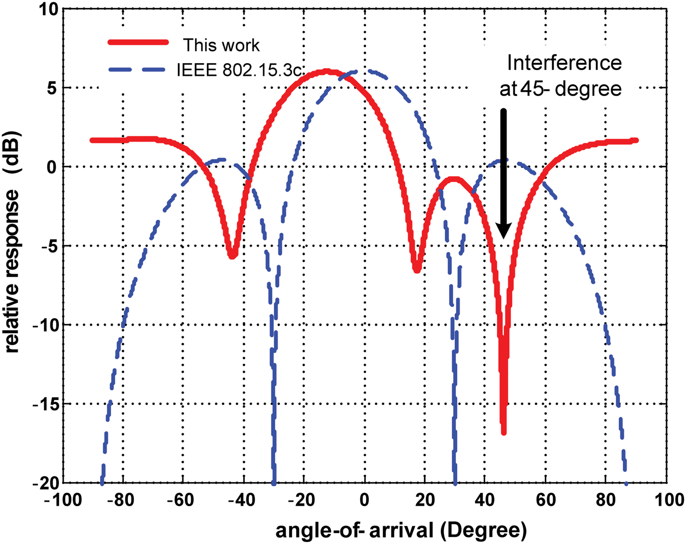
Fig. 2. Comparison between interference mitigation of the proposed architecture and the IEEE 802.153c 2-bit beam-forming.0
B) Phase shifting element architecture
There are three major categories of the phased-array architecture depending on the position of phase shifters in the system. Silicon mm-wave phased-array systems with Local Osillator (LO) phase shifting architecture have been introduced in [Reference Guan, Hashemi and Hajimiri7, Reference Natarajan, Komijani and Hajimiri11]. In order to make the phase shifting in the LO path less power hungry and less complex many techniques have been introduced such as injection-locked oscillators and phase shifting in lower frequency. In this case, a frequency multiplication stage should be employed to generate the required LO signal as in [Reference Natarajan, Komijani, Guan, X.; Babakhani and Hajimiri12–Reference Buckwalter, Babakhani, Komijani and Hajimiri18]. IF and baseband phase shifting have been reported in [Reference Kishimoto, Orihashi, Hamada, Ito and Maruhashi19, Reference Raczkowski, De Raedt, Nauwelaers and Wambacq20] and RF phase shifting architecture in [Reference Koh and Rebeiz21–Reference Reynolds, Natarajan, Tsai, Nicolson, Zhan, Duixian, Kam, Huang, Valdes-Garcia and Floyd27]. Bidirectional RF phase shifting 32 channels phased-array transceiver has been reported in [Reference Cohen, Jakobson, Ravid and Ritter28]. RF phase shifting and combining architecture has the lowest silicon area and power consumption and minimum number of extra components. The main challenge in realizing the RF phase shifting is the design implementation of a high performance RF phase shifter and the low loss RF power combining network.
Table 1. State-of-the-art silicon mm-wave phased-array receivers.

The RF phase shifting and combining architecture exhibits the lowest silicon area and lowest number of added components. This translated to lower power consumption. However, the performance of the receiver front-end in terms of noise, linearity, and gain and power consumption is directly affected by the performance of the phase shifter. Friis's equation for cascaded noise factor shows that if the LNA gain is close to 20 dB, the effect of the following stages can be neglected. So the noise figure is not the main affecting factor, the power consumption of passive phase shifters is lower but the insertion loss is not constant versus phase shift, and this leads to array gain variation. To compensate this effect, variable gain amplifier (VGA) is needed. This results in a similar power dissipation of the vector modulator to the passive phase shifter with VGA. Vector modulator phase shifter has been chosen to be implemented in this front-end.
C) Receiver architecture
The 60 GHz phased-array receiver front-end presented in this paper is designed to be compatible with the sliding-IF super-heterodyne architecture as shown in Fig. 1. It consists of eight RF phase shifting front-ends. Each contains a three-stage fully differential common-emitter LNA and an mm-wave vector modulator. The LNA is featuring 18 dB of gain and 6.8 dB of Noise Figure (NF) and detailed schematic and description of the LNA can be found in [Reference Sun, Borngraber, Herzel and Winkler29]. A fully differential power combining network is used to combine outputs of each receiver element, and feed the signal to a down-conversion mixer that performs frequency down-conversion from 60 GHz RF to 12 GHz IF with 48 GHz LO generated from a fully integrated frequency synthesizer. The down-conversion mixer is based on Gilbert's cell structure as in [Reference Sun and Glisic30]. The on chip integrated PLL described in [Reference Herzel, Glisic and Winkler31] generates the LO signals for both RF and IF down-conversion stages. The integrated 48 GHz VCO drives the mixer and is divided by four divider chains to generate the required 12 GHz, I/Q signals to drive the demodulator. To characterize the performance of the phased-array receiver at 60 and 12 GHz, an active power divider is inserted between the active power combiner and down-conversion mixer.
III. VECTOR-MODULATOR DESIGN
As discussed earlier, in order to adjust beam pattern for interference mitigation, both amplitude and phase control are necessary. This section describes the design of the mm-wave vector-modulator. Main requirements of the RF vector-modulator for receiver applications are low insertion loss to minimize the noise figure of the receiver and high linearity to avoid saturation by large interference. Particularly, the vector-modulator should also have low phase and amplitude errors to avoid beam distortion, resulting in lowered antenna gain within the angle of interest [Reference Valdes-Garcia, Nicolson, Lai, Natarajan, Chen, Reynolds, Zhan, Kam, Liu and Floyd26]. Figure 3 shows the block diagram of the proposed vector-modulator. It consists of an in-phase and quadrature (I/Q) generation network to split incoming differential RF signals into I and Q paths. The amplitudes and polarities of I and Q paths are controlled independently using VGAs which invert the phase. By summing the outputs of the VGAs, the resultant vector can be allocated freely in the entire complex plane. The ideal gain and phase transfer functions of the vector-modulator are given in (1) and (2), respectively. Where A I and A Q are the amplitude weights of I and Q
 $$G = \sqrt {\left\vert {A_{\rm I} } \right\vert ^2+\left\vert {A_{\rm Q} } \right\vert ^2 }$$
 $$\varphi = \arctan \left({\displaystyle{{A_{\rm Q} } \over {A_{\rm I} }}} \right)$$
Since the output phase depends on the gain ratio between I and Q paths, phase errors come not only from the phase mismatch between I and Q branches but also from the gain mismatches. It could be compensated by adjusting VGA gains. However, this will increase the complexity of the control circuits of the VGA.

Fig. 3. Block diagram of the mm-wave vector-modulator.
In modern phased-array chips, digitally controlled phase-shifters are a must. In order to make the control circuits and Digital to Analog Converters (DACs) as simple as possible, minimization of I/Q gain and phase-error are critical. The design procedure of the mm-wave vector-modulator which is suitable for a phased-array receiver can be summarized in few simple steps. The first step is to design the I/Q generation network, which exhibits low insertion loss and low I/Q imbalance. Step two is to optimize the VGA core to support the four quadrants. Finally, an output matching network should be designed to provide lowest amplitude and phase changes.
A) 90° hybrid coupler design
In vector-modulators, I/Q generation can be achieved by an all-pass polyphase filter [Reference Koh, May and Rebeiz22, Reference Sarkas, Khanpour, Tomkins, Chevalier, Garcia and Voinigescu32], 90° transmission lines [Reference Yikun, Baltus, van Roermund, de Graauw, van der Heijden, Collados and Vaucher25] or quadrature coupler [Reference Tsai and Natarajan33]. The quadrature hybrid coupler is chosen for this design because it offers low insertion loss, easy matching to 100 Ω differential transmission lines, and low I/Q amplitude and phase errors. Hybrid coupler can be constructed from two coupled lines if their length is a quarter-wave length. Coupled transmission lines can be implemented as edge- or vertical-/broadside-coupled lines. Edge-coupled Lange couplers operating at 60 GHz have been reported [Reference Tsai and Natarajan33]. Vertical coupled lines and couplers have reported in [Reference Sawicki and Sachse34]. However, it is challenging to implement broadside coupler in silicon technologies, due to the conductive substrate, high ohmic loss in the conductors, and the limited height of interlayer silicon dioxide. In this work, a broadside differential 3-dB hybrid coupler was implemented using in-house SiGe BiCMOS technology with five metallization layers. To achieve high coupling efficiency, 3rd and 4th metal layers were used, where inter-layer distance is 0.9 µm while the lowest metal layer was employed as the ground for the microstrip lines. The metal stack of the used technology is shown in Fig. 4.

Fig. 4. Metal stack of the used technology.
The overall coupler consists of two identical 90° single-ended vertically stacked broadside hybrid couplers as shown in Fig. 5: the two couplers are fed from port one through a 100 Ω differential transmission line, which is implemented in the top most metal layer with conductor width of 3.5 and 4.5 µm spacing. The single-ended hybrid coupler is meandered to save the area. The in-phase outputs of the two single-ended couplers are connected to port 2 to form the differential I signal, similarly the quadrature outputs are connected to port 3. It is clear from Fig. 5 that port 2 is implemented in the 2nd top metal layer while port 3 is in 3rd metal layer. The overall coupler structure is symmetric around the input lines.

Fig. 5. Hybrid coupler physical constructions.
The single-ended coupler is realized using vertically stacked broadside coupled lines, the length of the lines is optimized to be λ/4 at 60 GHz. Due to the vertical nature of the structure, the distributed capacitance between the lines is different from the one between the bottom line and the ground. The capacitance between the two coupled lines C1 as shown in Fig. 5 is much higher than the capacitance between the lines and the ground C2. The width of the lower line is chosen to be wider than the top line in order to enhance the coupling: the fringing field from the top conductor intersects the lower one. This will result in higher coupling, which is around to −3.5 dB. The width of both lines are optimized to achieve the desired odd and even mode characteristic impedances (Z0o, Z0e) which are 22 and 120, respectively, to achieve 50 Ω impedance of coupler. The top line width is 5 µm and the lower line width is 8 µm. In the odd mode, the capacitance between the two lines C1 will be much higher than the capacitance to the ground C2 which will result in low impedance. On the other hand, in even mode, where C1 will be almost zero because the two lines have the same potential then the dominant capacitance will be C2 which is small enough to achieve high even mode characteristic impedance. Finally Electromagnetic (EM) simulations were carried out to optimize the performance of the coupler in terms of coupling, amplitude imbalance, and 90° phase shift.
Finally, the two single-ended couplers, the feed lines, and the output connection lines are fully EM simulated with ADS momentum, to optimize odd-mode and even-mode characteristic impedances (Z0o, Z0e), where the required Z0e and Z0o are 240 and 42 Ω, respectively, which results in 100 Ω differential impedance at the input and output ports. Also the connection lines between the ports and the couplers are optimized for best phase error. Fig. 6(a–c) shows the simulated characteristics of the hybrid coupler. The difference between the |S21| and |S31| is plotted in (b) and it ranges from 0.9 to 1.2 dB from 50 to 70 GHz, in this design the amplitude difference is sacrificed to be moderate to achieve very low phase mismatch of 2°.

Fig. 6. (a) Simulated performance of the coupler, both amplitude and phase difference, (b) S11, S22, S33 of the coupler, and (c) S21, S31 of the coupler.
B) Vector-modulator core
The VGA employed in this design is similar to the double-balanced Gilbert cell. Figure 7 shows the detailed schematic of the active core of the designed vector-modulator. It consists of two VGAs sharing the resistive load R1 and R2. Gain control of a single VGA is achieved though differential analogue control voltages by steering the current though transistors quads Q 3, Q 4, Q 5, and Q 6. The differential control voltage is generated from a differential pair as depicted in Fig. 7; The VGA gain without linearization is given by (3):
 $$\displaystyle{{v_{{\rm out}} } \over {v_{{\rm in}} }}=2g_{m1} R_1 \times \tanh \left({\displaystyle{{V_{{\rm con}} } \over {2V_T }}} \right)$$
where g m1 is the transconductance of Q 1 and Q 2, V con is the differential control voltage applied at the bases of Q 3, Q 4, Q 5, and Q 6, and V T is the thermal voltage. Since the gain is related to control voltage with hyperbolic tangent function, the control voltage should have very slow change for linear control. The amplifiers used for this control were linearized with high emitter resistor. R C is chosen to be 220 Ω and R E is 650 Ω to give maximum output voltage swing of 0.3 V, which is enough to control VGA gain.

Fig. 7. Detailed schematic of the mm-wave vector-modulator.
Since the current is steered in the quads Q 3, Q 4, Q 5, and Q 6 it becomes constant in the main differential pair Q 1 and Q 2. As a result, input matching and the linearity of VGAs do not significantly change with gain variation. The main differential pair transistors were chosen to have 3.4 µm emitter widths, with input impedance of 55-j45 Ω, requiring only 120 pH inductor to match the input impedance of the transistor to 50 Ω. The bias current of Q 1 and Q 2 is chosen to have 80% of the maximum f T current as a compromise between power consumption and differential pair gain. The output currents of two VGAs are combined in output nodes. As the current is steered in the VGA quads (Q 3–Q 6) and (Q 9–Q 12), the parasitic capacitance at the output nodes (collectors of the Hetero-junction Bipolar Transistor (HBT)) changes with the gain setting of the two VGAs. To easily calculate this effect, the simple small signal equivalent circuit for common base amplifier is shown in Fig. 8. Assuming that r b is very small. The output current can be rewritten as
 $$i_{{\rm out}}=- g_m v_1+v_{{\rm out}} sC_\mu$$
 $$v_1=- \lpar i_{{\rm out}} - v_{out} \times sC_\mu \rpar \times \displaystyle{{R_s sC_\pi } \over {R_s sC_\pi+1}}$$
Fig. 8. Small signal equivalent circuit for common base amplifier.
By solving (5) for i out and substitute in (4), the output impedance can be calculated as
 $$Z_{{\rm out}} \approx \displaystyle{1 \over {j\omega \lpar C_\mu+C_{CS} \rpar }}$$
where R s is the source output impedance, C CS is the collector substrate capacitance, and C μ is the base collector junction capacitance defined as
 $$C_\mu=\displaystyle{{C_{\mu 0} } \over {\left[{1 - \lpar V_{{\rm BC}} /\psi _o \rpar } \right]^n }}$$
where C μ0 is the base collector junction at zero bias, while V BC is the base collector voltage. It is clear that the output impedance at high frequencies is dependent on the bias voltage. By applying the same concept to the output node of the VGAs, The total output impedance of single VGA can be easily calculated as
 $$C_{{\rm out}}=\displaystyle{{\lpar C_{{\rm out}3}+C_{{\rm out}5} \rpar \times \lpar C_{{\rm out}4}+C_{{\rm out}6} \rpar } \over {\lpar C_{{\rm out}3}+C_{{\rm out}5} \rpar +\lpar C_{{\rm out}4}+C_{{\rm out}6} \rpar }}$$
 $$Z_{{\rm out}} \approx \displaystyle{1 \over {j\omega C_{{\rm out}} }}$$
Equations (8) and (9) show that the output capacitance of the VGAs is changing with control voltage change. The change of the total capacitance of the output node of the vector-modulator will depend on the location of the vector in the complex plan as depicted in Fig. 9(a). To accurately determine the output impedance of the vector-modulator; the inter-connects between the transistors have been EM simulated using ADS momentum. Then both inter-connect and transistors are used to simulate the S-parameters. The simulated S22 of the vector-modulator is plotted in Fig. 9(b). The output impedance is changing with the phase state. From the output impedance, output capacitance is calculated and it is found to be changing between 83–93 fF. Using the L-section L-C load network to match the output impedance to 100 Ω, the required L is found to be 92 pH while the capacitor is 10 fF. The matching capacitor is very close to the amount of change in the output capacitance, this changing capacitance resonates with the load inductor. This would result in high amplitude and phase variations as shown in Fig. 9(c). In order to minimize it, resistive loads were used to achieve very low amplitude and phase changes as plotted in Fig. 9(d). A small buffer amplifier was employed to enhance the matching to the following 100 Ω differential transmission line. The phase shifter draws 12 mA from 3.3 V supply, and exhibits a 1 dB compression point of −7 dBm.

Fig. 9. (a) Shows how VGAs capacitances changes with output vector location. (b) Shows the simulated variations in the vector-modulator's output impedance. (c) Polar plot of the S21 of the vector-modulator with L-C network. (d) Polar plot of S21 of the vector-modulator with R-C network.
IV. POWER COMBINING NETWORK DESIGN
A) Architecture
The design of the mm-wave power combining networks is a challenging task because it has different constraints such as power dissipation, insertion loss, silicon area, bandwidth, and linearity. A series combining topology promises the minimum routing of the mm-wave signals, however, it results in a low 1 dB compression point as a result of cascading multiple active circuits. Power combining trees with multi-step combining suffers from higher insertion loss due to long mm-wave lines but it offers higher linearity and lower power dissipation. A passive device such as, Wilkinson power combiner has the lowest power dissipation but consumes a large silicon area. Active power combiners provide intrinsic gain at the cost of the limited linearity and increased power consumption of the receiver front-end. The presented hybrid passive and active power combining network schematic is depicted in Fig. 10. Passive Wilkinson combiners were implemented as the first combining stage to combine each two adjacent channels in order to achieve high isolation between the adjacent elements. It is followed by 100 Ω differential microstrip lines. Those lines drive the four-to-one active power combiner, which provides gain for combined signals while maintaining isolation. Ideally, the stage with better linearity should be the last stage, but the insertion loss of the passive Wilkinson power combiner will enhance the linearity of the later stage which is the active combiner. In other words, the active combiner saturates faster if it was inserted after the vector modulator. The input impedance of the Wilkinson power combiner is constant with respect to the input signal level, so the vector modulator is always loaded with constant impedance; this is not the case if the active combiner is following the vector-modulator. Finally using active power combiner after the vector-modulator leads to an increase in the number of active components, and this leads to higher power consumption. For those three reasons, the Wilkinson power combiner is decided to be the second stage after the vector-modulator, while the active combiner is used to combine the output of the four Wilkinson combiners.

Fig. 10. Block diagram of the hybrid passive-active power combining network.
B) Circuit level design
Fully differential Wilkinson power combiners are employed to combine the output of two front-ends. It was implemented in the top most metal layer of our in-house IHP 0.25 µm BiCMOS technology, while the lowest layer is assigned to the ground layer. Differential microstrip transmission lines were employed to construct the combiner as in [Reference Elkhouly, Chang-Soon Choi; Glisic, Scheytt and Ellinger35]. EM simulations show that Wilkinson power combiner exhibits <0.7 dB insertion loss and more than 25 dB isolation. The designed active power combiner combines the outputs of the four Wilkinson power combiners. It is based on current-summing cascode amplifiers. Inductive loads are utilized to match the output impedance to 100 Ω differential transmission lines. In total 110 pH inductors were used to match the input impedance of the cascode amplifiers to the output impedance of Wilkinson combiners as illustrated in Fig. 11. The combiner draws 24 mA from 3.3 V supply, each channel exhibits 7 dB of gain and an input 1 dB compression point of −5 dBm. We designed an active power divider; it consists of cascode amplifier and an mm-wave transformer used as load. The secondary winding of the transformer is divided into two sections; the induced current will be divided evenly between the two sections of the secondary windings but with 180° degree phase shift. By inverting the output terminals of one section, the divided signals will have the exact amplitude and phase. The transformer was implemented on metals 3 and 4, because they have 1 µm vertical separation and this increases the coupling between secondary and primary windings. Figure 12(a) shows the physical geometry of the transformer divider and Fig. 12(b) illustrates the simulated performance of the divider. It shows that the designed active divider exhibits <1.5 dB insertion loss with almost ideal amplitude and phase match. The plotted S-parameters of the transformer are referenced to the −3 dB of division loss, to illustrate the loss of the transformer windings only. The schematic of the active divider is plotted in Fig. 13. It consists of a cascode amplifier loaded with the transformer divider. Small MIM capacitors are used to tune the inductive load of the amplifier and to match the output impedance to the 100 Ω differential transmission lines. One branch is fed to on-wafer GSGSG probe pads and the other is connected to the down-conversion mixer through long 100 Ω differential transmission line.

Fig. 11. Schematic of the 4 to 1 active power combiner.

Fig. 12. 60 GHz transformer divided (a) physical construction of the transformer (b) simulated performance of the transformer, divider insertion loss, and insertion phase.

Fig. 13. Active power divider schematic.
V. MEASURMENTS RESULTS
The phased-array receiver chip was fabricated in IHP's 0.25 µm SiGe BiCMOS technology, which offers HBT with f T/f max = 180/200 GHz and five metal layers. Figure 14 shows the receiver chip micrograph. The overall chip size is 2.9 × 4.2 mm2. The discrete active modulator and the active power divider also were fabricated for test purposes. The fabricated chips were characterized with different setups; a 4-port vector network analyzer (VNA) system is used to measure the S-parameters, whereas signal generators and spectrum analyzer are used to measure the 1 dB compression point.

Fig. 14. Phased-array chip micrograph.
A) Active power divider measurements
Figure 15 depicts the measured S-parameters of the active power divider test structure. The power gains S21 and S31 are shown with 4 dB at 56 GHz and 3 dB at 66 GHz. The measured gain of the divider is 1.5 dB lower than the simulation results due to layout parasitic and device and process variations. It is also possible that the EM simulation did not predict the series resistance of the transformer windings, which affect the quality factor and the insertion loss of the transformer especially at the resonance frequency. And this is translated into higher gain difference at the peak frequency and lower error at frequencies away from the resonance. The input and output return losses (S11 and S22) are less than −15 dB at 56–68 GHz. Both phase and amplitude of S21 and S31 are identical, which makes the designed power divider ideal for phased array systems. The active divider draws 5 mA from 3.3 V supply.

Fig. 15. Active power divider simulated and measured performance, both amplitude and phase.
B) Single element measurements
The measurement was taken by connecting the first port to the input of the LNA of one channel and the second port to the output from the active power divider, which is the RF output as marked in chip micrograph. The measured S-parameters of four different channels all set to the same phase and amplitude state are plotted in Fig. 16. The S21 is 18.5 dB at 57.5 GHz, while a 2.5 GHz frequency shift of the centre frequency compared with the simulated performance was observed. The 3 dB bandwidth is 5 GHz. The main reason of this frequency shift is the limited accuracy of the active device models and the layout parasitic in the active power combiner. In the final design testing of the RF and IF performances will not be needed, so the active power divided can be eliminated. This will increase the bandwidth of the front-end to 8 GHz. Input return loss S11 is less than −10-dB in the band 50–70 GHz and the output return loss S22 is close to −10 dB.

Fig. 16. Measured S-parameters of the four channels of the phased-array receiver chip.
For testing the vector-modulator of each channel, both control voltages were swept and S-parameters were measured for every state, the S21 of all states are plotted in Fig. 17. It is clear that the vector modulator exhibits both amplitude and phase control, and it also offers extremely low amplitude and phase variations. This comes from the resistive loads in the vector-modulator core, both 3 dB attenuation and 6 dB attenuation circles are marked in the same figure. Sixteen different states with phase step of 22.5° and constant amplitude were also measured to compare the presented phase shifter with previously published 4-bits phase shifters [Reference Koh, May and Rebeiz22, Reference Koh and Rebeiz37]. Figure 18 illustrates the 16 states of relative phase shift of one channel. Figure 19 shows RMS gain and phase errors from the ideal states for the three amplitude states maximum, 3 and 6 dB attenuations. The RMS gain error and phase error for different amplitude states show that the vector-modulator exhibits low phase and amplitude variations for different amplitude states. The measured RMS phase error is <5°, while the RMS amplitude error is <0.9 dB between 55 and 67 GHz. Figure 20 shows the output power at IF and RF ports, as a function of RF input power at 57.5 GHz. The measured input referred P1 dB of one receiver channel is −22 dBm at the highest gain state of the vector-modulator.

Fig. 17. S21 Polar plot of one channel, showing both phase and amplitude control in the vector modulator.

Fig. 18. Measured relative phase shift of one element for the 16 states.

Fig. 19. Measured RMS gain and phase error of the 16 states.

Fig. 20. Measured 1 dB compression point for both RF and IF outputs.
C) Phased-array measurements
The gain and phase mismatches between array channels were measured by comparing the reference state (maximum gain) S-parameters of all the eight channels (S21, S31, S41, S51, S61, S71, S81, and S91). The chip exhibits <0.5 dB of RMS gain mismatch and <4° of RMS phase mismatch between different channels as plotted in Fig. 21. The low gain and phase mismatches between the different channels are attributed to two reasons: first, the near perfect symmetry of the mm-wave power combining network. Second, the uniform distribution of the supply lines for both the LNAs and the vector-modulators. During the layout of the phased-array chip, careful attention was given to the mm-wave combining network layout. By using exactly the same differential transmission lines between different front-ends and Wilkinson combiners. The layout of the active power combiner is kept symmetric by minimizing transmission lines cross-over. DC power distribution grid was utilized to supply different blocks with supply voltages. Metal stacks of 25 µm width and 5 µm thickness are used to distribute the current to minimize the IR drop and ensure that all receiver elements get the same supply voltage. The phased-array beam pattern was calculated from the measured S-parameters sets of all eight channels as follows. In order to construct the model shown in Fig. 22, the gains of the combining network under single-port excitation and eight ports excitation scenarios are calculated from the simulation. This will show the gain difference between the two cases. This gain difference will be taken into account in a power combiner model. The created model is then simulated and compared with the full-chip transistor level simulation to ensure the models accuracy. Finally, simulation of the created model is used to calculate the array beam pattern by changing the angle of the reception and plotting the output power under the following assumptions: the each channel is connected to isotropic antenna and the antenna spacing is λ/2 at 60 GHz. To measure the power combining of two different receiver channels, we established the measurement setup as illustrated in Fig. 23. RF input signals were divided and connected to two different inputs of the receiver elements. The phase setting of one channel is held constant, while the other ones is varied in 10° steps, the measured IF power is plotted versus the phase shift angle of the 2nd channel. It is shown in Fig. 24, the output power reaches the maximum when the two signals are in phase and it is attenuated be 30 dB as they become out of phase.

Fig. 21. Measured amplitude and phase mismatch between the different channels.

Fig. 22. Measurments-based simulation model of the phased array chip.

Fig. 23. Measurements setup for two channel-combining characterization.

Fig. 24. Power-combining response with one element phase is swept while the other is held constant.
D) Interference mitigation demonstration
To conduct experimental verification for interference mitigation, the chip must be integrated with the antennas. Currently, we are working in the design of a module including the chip and eight antennas and IF chip, both LTCC and multi-layer RF board are considered for the manufacturing process. The module design and the manufacturing process require long time, that is why we tried to build the simulation model based on the measured data so it will be faster to verify the interference mitigation. To demonstrate interference mitigation capability of the presented phased-array front-end, a simulation model based on measured data has been built in ADS. It contains the measured S-parameters file of the eight elements connected together to form the phased-array receiver. The model also contains two transmitters, one representing the desired signal and the other representing the RF interferer transmitter. The angle of the arrival of the RF interferer transmitter can be changed within simulation as shown in Fig. 25. The eight phase shifters are adjusted to receive the desired signal from 90° direction. By sweeping the angle of the interferer and observing the output signal. The simulation results are plotted in Fig. 25. By changing the amplitude weighting vector from [1,1,1,1,1,1,0.5,1] to [1,1,1,1,1,1,0.5,1.5] and keeping the phase shift constant, the position of minimum interferer can be changed as shown from 74 to 114°. The interferers have around 25 dB of SINR. As demonstrated that the position of minimum interferer can be changed by changing the amplitude weights of the different channels which provides more flexible interference suppression for the 60 GHz receiver. In the presented simulation model, the maximum interference level is limited up to −25 dBm; this will ensure that vector modulator nonlinearities will not generate intermodulation products. At this power level, the LNA is in linear region and it will not affect the phase of the signal hence the LNA 1 dB compression point is −10 dBm. The vector-modulator architecture itself has the advantage of almost constant phase state with respect to the input power level as power is less than the 1 dB compression point which is −7 dBm. By taking those assumptions into consideration the antenna beam pattern will not change with the interferer power level as long as it is close to −25 dBm. Table 1 summaries the performance of the recently published phased-array receivers.

Fig. 25. Interference mitigation simulation model and results.
VI. CONCLUSION
In this work, a 60 GHz band eight-element phased-array receiver with RF vector-modulator has been presented. It enables 360° phase control range and more than 20 dB amplitude control for each receiver channel. In addition, it exhibits 16 dB of gain at 60 GHz and −22 dBm input referred P1dB compression point. The 3 dB bandwidth of the entire receiver front-end is 5 GHz, and it can be further increased to 8 GHz if the active power divider that was inserted for test purpose is removed. The chip exhibits <0.5 dB and <4° amplitude and phase mismatch between different channels. Interference mitigation technique is also presented and verified by a simulation model based on measurements data. It exhibits 25 dB of SINR. The measured performance of the presented phased-array chip verifies its suitability for highly integrated beam-shaping array with interference cancellation capabilities. In future designs, the current LNA can be replaced by low power LNA in [Reference Sun and Scheytt38] and this will reduce the power dissipation to 36 mW.
ACKNOWLEDGEMENT
The authors would like to thank Christian Wipf and Johannes Borngraber for wafer characterization. We also would like to thank IHP pilot staff for the chip fabrication.
 Mohamed Elkhouly received his B.Sc and M.Sc. both in electronics and communication engineering from Ain Shams University, Cairo, Egypt in 2003 and 2008, respectively. In 2008, he joined IHP as a researcher in the microwave and millimeter-wave group, where he participated in the design of 60 GHz transceivers. His current research interest include, but are not limited to, microwave and millimeter-wave beamforming circuits with special emphasis on RF phase shifters and on-chip power distribution and combining networks.
 Chang-Soon Choi received B.S., M.S., and Ph.D. degree in electrical and electronic engineering from Yonsei University, Seoul, Korea, in 1999, 2001, and 2005. His doctoral dissertation concerned fiber-supported millimeter-wave wireless communication systems. From 2005 to 2007, he was with the National Institute of Information and Communications Technology (NICT), Japan, where he developed millimeter-wave wireless communication systems and microwave photonics systems. In 2007, he joined the IHP microelectronics GmbH, Germany, to develop 60-GHz wireless LAN systems, particularly multi-Gbps OFDM and millimeter-wave beamforming. He also contributed to the IEEE 802.11ad and IEEE 802.15.3c standardization activities. He is now with NTT DoCoMo Communications Laboratories Europe GmbH, Munich, Germany, where he has been involved in the development of cooperative network MIMO systems for LTE-Advanced applications.
 Srdjan Glisic received his B.S. degree in electrical engineering from the Faculty of Electronic Engineering, Nis, Serbia in 2000. He joined Circuit Design Department of IHP, Frankfurt Oder, Germany in 2003. He is involved in projects on 60 GHz wireless communication and automotive radar in 77 GHz frequency range. He works mainly on VCOs, PLLs, Pas, as well as PCB design and system integration.
 Frank Ellinger (S'97-M'01-SM'06) was born in Friedrichshafen, Germany, in 1972. He graduated in electrical engineering (EE), in 1996 from the University of Ulm, Germany. He received an MBA and a PhD degree in EE from the ETH Zürich (ETHZ), Switzerland, in 2001, and the habilitation degree in high-frequency circuit design from the ETHZ in 2004. Since August 2006, he is full professor and head of the Chair for Circuit Design and Network Theory at the Dresden University of Technology, Germany. Currently, he is member of the management board and coordinator of the communications area in the German excellence cluster project Cool Silicon. From 2001 to 2006, he was head of the RFIC design group of the Electronics Laboratory at the ETHZ, and a project leader of the IBM/ETHZ Competence Center for Advanced Silicon Electronics hosted at IBM Research in Rüschlikon. Prof. Ellinger has been the coordinator of the EU funded projects RESOLUTION and MIMAX. He has published more than 170 refereed scientific papers, most of them are IEEE journal contributions, and holds three patents. Prof. Ellinger authored the lecture book “Radio Frequency Integrated Circuits and Technologies” published by Springer. He has been elected by the IEEE MTT S as IEEE Distinguished Microwave Lecturer for 2009–2011. For his works, he received several awards including the IEEE MTT-S Outstanding Young Engineer Award, the ETHZ Medal, the Denzler Award, two times the Rohde&Schwarz/Agilent/Gerotron EEEfCOM Innovation Award, and a Young PhD Award of the ETHZ.
 J. Christoph Scheytt received his diploma degree (1996) and PhD degree (2000, with highest honors) both from Ruhr-University Bochum, Germany. In 2000, he co-founded advICo microelectronics GmbH, a German IC design house. For 6 years, he served as CEO at advICo where he was responsible for various projects in the area of wireless and fiber-optic IC design. Since 2006, he is with IHP where he is head of circuit design department, a group of about 30 researchers working on high-frequency and broadband IC design. His research interests include RFIC and broadband IC design, PLL techniques, and design of SiGe BiCMOS technologies.


