


I. INTRODUCTION
Since early investigations of hybrid Tee-junctions [Reference Kahn1], a great deal of studies have been conducted aiming to analyze [Reference Marcuvitz2], improve [Reference Arnold, Lyon, Schlaud, Solbach and Tanner3], and optimize [Reference Yao, Abdelmonem, Liang, Liang, Zaki and Martin4, Reference Christopher, Abid Hussain, Easwaran and Dabade5] this structure. The reason for this constant interest is the wide range of applications of this power divider. Indeed, the Tee-junction has become an essential component in microwave and millimeter-wave systems such as multiplexers, couplers, antenna feed networks, etc. [Reference Hirokawa, Sakurai, Ando and Goto6, Reference Wu, Deslandes and Cassivi7]. Traditionally, these components have been based on rectangular waveguides, which prevent them from being used in highly integrated and low-cost applications. However, by using substrate integrated waveguides (SIWs), it has been possible to construct such devices in planar substrates by using PCB technology. SIWs, proposed in [Reference Hirokawa and Ando8], are waveguides that may be synthesized in planar substrates by using metallic posts to construct lateral walls. An important number of microwave and millimeter-wave components have recently been developed based on this technology, including Tee-junctions [Reference Huang and Lu9, Reference Yang and Fathy10].
SIWs are especially attractive for antenna feeding because they make it possible to integrate the radiating elements and circuits in the same substrate [Reference He, Wu, Hong, Han and Xiao-Ping11]. For such feeding systems, unequal power dividers are essential to satisfy stringent pattern characteristics, high directivity, and low side-lobes required in radars and satellite communications.
In this paper, a detailed procedure is proposed to design SIW Tee-junctions with wide-range split-power ratio and phase-balanced outputs. Furthermore, it is shown how these junctions may be connected to obtain 1 → 2N unequal power dividers. The proposed methodology is remarkably convenient because it details how to set the junction parameters for power split ratios varying from 1:1 to 1:8 without performing any simulations. The structure parameters, as proposed in this paper, guarantee input matching better than 18 dB; besides, they can be set as starting values for eventual optimizations.
The SIW Tee-Junction structure used in this paper is inspired by the one presented in [Reference Arnold, Lyon, Schlaud, Solbach and Tanner3]. This model was also used in [Reference Yang and Fathy10] to develop a graphical procedure for Tee-junctions design with arbitrary power division ratio; however, the maximum ratio achievable with such a method is 1:2.8, which is excessively limiting for system designs requiring unequal power division. To provide a solution to this issue, the method proposed in this manuscript presents several novelties: (a) the power division ratio range is significantly wide, it goes from 1:1 to 1:8, (b) range extension of the power division ratio is achieved by introducing a new parameter with respect to [Reference Yang and Fathy10], which is the central post diameter, (c) in [Reference Yang and Fathy10], no compensation of the output phase imbalance generated by unequal power division was presented, (d) an implementation example illustrates the process to build 1 → 2N dividers to satisfy an arbitrary power division law by using Tee-junctions as a fundamental block.
The rest of the document is organized as follows. Section II presents the basic SIW structures making up the power divider. Then, in Section III, the design methodology is explained and detailed in several steps. Three implementation examples at different frequencies are presented in Section IV to illustrate the design procedure and to demonstrate its accuracy through the obtained results.
II. TEE-JUNCTION STRUCTURE
A) SIW Tee-junction
The SIW Tee-junction model is presented in Fig. 1. It is made up of equal size rectangular waveguides, so that only the TE10 mode is supported. The power split ratio is controlled by placing a septum and an iris is used to minimize the return loss. The SIW width is denoted by a and is measured between the central points of two opposite side-wall posts. The diameter and spacing between two consecutive posts are denoted by d and s, respectively. Traditionally, in rectangular waveguide Tee-junctions, the central post is used for input matching [Reference Hirokawa, Sakurai, Ando and Goto6]; however, in this case, it is used to replace the septum. Hence, the central post diameter d C and its position (l, h) modify the power split ratio.

Fig. 1. Unequal power Tee-junction with phase-unbalanced outputs.
Similarly, the iris used for insertion loss improvement in [Reference Arnold, Lyon, Schlaud, Solbach and Tanner3] is constructed by shifting the last posts of the input port by t. Unequal power division leads to phase-unbalanced outputs, which may be compensated for by shifting the input port by p from the central line 0X, as illustrated in Fig. 2.

Fig. 2. Tee-junction of Fig. 1 with phase compensation.
B) Microstrip–SIW transition
In order to integrate the SIW power dividers with packaged circuits, microstrip lines, or coplanar components, appropriate transitions are required. For the implementations presented in this paper, microstrip transitions were needed to measure their performances.
Recently, microstrip to SIW transitions have been the subject of a significant number of studies [Reference Huang, Wu and Ehlert12–Reference Ding and Wu14]. The structure proposed in [Reference Deslandes and Wu15] was chosen for this application because of its low insertion losses, wide bandwidth and implementation simplicity.
C) SIW 90° bend
To implement 1 → N power dividers, corporate architecture is preferred over serial architecture because of its wider bandwidth. In consequence, the type of dividers for which this methodology applies is 1 → 2N. To build such dividers, Tee-junctions are assembled and the use of SIW bends is essential. The 90° bend used in this implementation includes an inductive post to reduce the bend's reflection. The post size is the same as the posts used to construct the waveguide walls; its position with respect to the 90° angle was optimized through 3D electromagnetic simulations.
III. DESIGN METHODOLOGY
This section describes the proposed procedure for SIW Tee-junction design. It is the result of a study developed on three SIW Tee-junctions designed to operate at different frequency bands: X, Ku, and K. When compared to the guided wavelength, the via size used to build lateral walls of the Tee-junctions is different for each implementation; however, they respect all the conditions described in [Reference Xu, Wu and Wu16] for SIW design. This proves the applicability of the procedure to any via size in agreement with the general SIW design procedures.
The methodology exposed in this section is split into several steps. First, the basic SIW parameters (a, d, and s in Figs 1 and 2) are determined. Then, the second step distinguishes among two different cases of power division to determine the central via diameter. Similarly, the position of the vias making up the input iris, and then the central via offset h (see Fig. 2), are determined in order to guarantee input matching. In step three, the central via parameter l is extracted from the set of curves generated through parametric simulation studies (Figs 5 and 6). Finally, the output phase imbalance is compensated for by shifting the input port.
Hereafter, the magnitude of the power difference between the output ports of the Tee-junction is expressed by ΔOut. Since this procedure is scalable, all of the parameters are referred to the SIW guided wavelength λ g = 2π/β, where β represents the propagation constant of the guided wave in the SIW.
A) SIW design
Let f be the central frequency of the design and f c denote the waveguide cut-off frequency. The proximity between the cut-off frequency and the central frequency determines the operation bandwidth. For the designs presented in this paper, the ratio f/f c = 1.5 is used; however, this criterion may be modified as required by the application without affecting the rest of the design procedure.
Dimensioning the waveguide is straightforward through the relation a RWG = λ C/2, where a RWG is the width of the rectangular waveguide with the required cutoff wavelength λ C.
In [Reference Cassivi, Perregrini, Arcioni, Bressan, Wu and Conciauro17], it was demonstrated that equivalent width a of a SIW may be determined by using:
 $$a=a_{RWG}+\displaystyle{{d^2 } \over {0.95 \cdot b}}\comma \;$$
where b denotes the substrate thickness and d is the via diameter as defined in Fig. 2. In [Reference Xu, Wu and Wu16], the authors study the leakage losses and dispersion characteristics of SIWs and provide design rules for appropriately choosing the via size and spacing or pitch.
B) Determining t, h, and d C
In order to set the parameters t and h so that input matching is guaranteed for different diameters of the central post, parametric studies were carried out on the electromagnetic (EM) full-wave simulator ANSOFT HFSS. Regarding t, it was observed that the value set for equal power division did not require significant modifications when varying the central via position or size; it is then recommended to set t as approximately λ g/60. On the other hand, the distance h to assure appropriate input matching was observed to be dependent on the central post diameter d C. For this reason, h and d C have to be set according to the desired power split ratio.
The central post diameter impacts both, the input matching and the maximum power split ratio achievable for the unequal power division case. A small central post improves input matching but hampers achievement of high power split ratios. As this study aims to cover a large power split ratio range, the design procedure distinguishes two cases: high and low power split ratios.
1) LOW POWER SPLIT RATIO
For the equal power division case, the central post diameter d C ≈ λ g/25 allows us to ensure input matching better than −20 dB over more than 35% bandwidth. Using this diameter, parametric studies were run in order to establish the maximum shifting (l) of the central post for which the input matching level was still better than −18 dB at the central frequency. It was found to be around λ g/10 for h = d C. However, in order to have input matching over a significant bandwidth, the central post shifting is limited to λ g/15. When d C and h are fixed, shifting the central post towards one of the output ports causes a linear variation on the difference between the amplitude of the output signals, when plotted in dB. The range of l from zero to λ g/14.7 covers the cases of power differences within the range 0 dB ≤ ΔOut ≤ 3 dB.
2) HIGH POWER SPLIT RATIO
Similarly to the previous case, parametric studies were used to find the Tee-junction configuration to achieve ΔOut higher than 3 dB and guaranteeing input matching better than −18 dB. It was found that, by setting d C = λ g/13 and h = d C/2, it is possible to obtain differences between the output ports within the range 3 dB ≤ ΔOut ≤ 9 dB. This corresponds to the central post shifting from λ g/18 to λ g/6. When shifting the central post beyond λ g/6, it considerably approaches to the input port lateral wall axis, causing an important degradation on the input matching.
Figure 3 is an example of the graphs generated during this analysis. It presents the input matching and the power split ratio as functions of the central post shifting l at the central frequency. In this case, the substrate relative permittivity is 3.55, the central frequency is 14.25 GHz and the guided wavelength is 14.83 mm.

Fig. 3. S 11 and power difference between the output ports (ΔOut) as functions of the central post shifting (l).
These curves were generated for the three SIW T-junctions designed to operate at different central frequencies: 8, 14.25 and 23 GHz. Then, the curves were normalized by the guided wavelength; Fig. 4 illustrates how the three of them perfectly fit. Equivalent results were obtained for the curves relating the phase difference between the output signals and the distance l. The same procedure was applied for the low power split ratio case (0 dB ≤ ΔOut ≤ 3 dB).

Fig. 4. Normalization of the three set of curves generated to determine the central post shifting for 3 dB < ΔOut ≤ 9 dB.
C) Determining the central post offset and the output phase unbalance
The graphs generated in the previous section make it possible to easily determine the post position for a desired power split ratio. Figure 5 provides the required offset for the central post to be shifted from the 0 X position (see Fig. 2) to get an arbitrary power split ratio within the range 0 dB < ΔOut ≤ 3 dB. The desired power difference, ΔOut, is represented on the left ordinate and the required normalized offset (l) on the abscissa. Besides, the right ordinate provides the phase difference between the output ports once the central post is shifted. This value, represented by Δθ, allows calculation of the phase compensation parameter p. Figure 6 provides equivalent information to Fig. 5 for power split ratio within the range 3 dB < ΔOut ≤ 9 dB.

Fig. 5. Required central post shifting l and resulting phase difference for 0 dB < ΔOut ≤ 3 dB.

Fig. 6. Required central post shifting l and resulting phase difference for 3 dB < ΔOut ≤ 9 dB.
Even if the case of SIW Tee-junctions with power split ratio higher than 9 dB is not included in these curves, it is possible to easily design them by using some principles derived from this methodology; however, electromagnetic simulations are required. An initial configuration is setting t around λ g/60, d C bigger than λ g/13 and h close to d C/2. Then, to obtain the desired ΔOut, the only parameter to modify during the simulation is l. Then, the phase compensation is achieved as explained in the next section.
D) Calculating the input port offset
The phase shift Δθ is related to the distance x traveled by an electromagnetic wave in a guided medium by
 $$\Delta \theta=\displaystyle{{2\pi x} \over {\lambda _g }}$$
Using (2) and the Δθ value obtained from the previous step, it is simple to compute the required input port offset p = Δθ·λ g/4π. Such offset is measured from 0 X towards the opposite direction to which the central post was shifted.
IV. IMPLEMENTED POWER DIVIDERS
In order to validate the proposed methodology, several Tee-junctions and power dividers at different frequencies were implemented. No optimization process was performed to improve their performance; only the graphical method described in the previous section was applied.
A) X band Tee-junction with ΔOut = 2 dB
The central frequency f is 8 GHz and the substrate used is Rogers 4003 with thickness b = 508 µm. The available technology allowed us to easily fabricate 0.6 mm diameter vias; the pitch s between them is 1.2 mm. For this central frequency, an appropriate SIW width is found to be 15.25 mm. The guided wavelength is 26.6 mm.
By following the guidelines presented in Section III(B), the parameters t, h, and d C are set to 0.446, 1.064 and 1.064 mm, respectively. Using the curves in Fig. 5, the distance l and the phase difference between the outputs are found to be 1.207 mm and 22.2°, respectively. The distance p is then calculated as 0.823 mm.
Measurements are presented in Fig. 7; the bandwidth at 18 dB return losses is 17.8%. The measured power difference between the output signals is 2.14 dB at the design frequency and its variation is lower than ±0.2 dB (±10% ΔOut) over 9% bandwidth; the phase difference is less than 1.7° over the same bandwidth. The isolation measured between the output ports is roughly −7 dB.

Fig. 7. Measured S-parameters for X band Tee-junction with ΔOut = 2 dB.
B) K band Tee-junction with ΔOut = 6 dB
The same substrate as in the previous example was used. The central frequency is 23 GHz; the via diameter is 0.305 mm and the pitch s is 0.61 mm. Proceeding as in the previous case, the parameters a, l, and p are found to be 5.36, 0.978 and 0.785 mm, respectively. The guided wavelength is 9.27 mm.
Measurements are plotted in Fig. 8. As in example A, the minimum return losses are not at the design frequency, which is not surprising since that is not the most important design criterion. Instead, the methodology was designed to achieve the required power split ratio with an input matching level equal to or better than 18 dB. The measured power split ratio is 5.92 dB at the design frequency and its variation is lower than ±0.6 dB (±10% ΔOut) over 10.3% bandwidth. Within such bandwidth, the output phase difference is lower than 1°.

Fig. 8. Measured S-parameters for K band Tee-junction with ΔOut = 6 dB.
C) Ku band 1 → 4 phase balanced unequal power divider
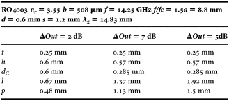
In order to respect particular radiation pattern constraints imposed for satellite communications, a SIW slot antenna array is required to be fed according to the power law in Table 1. The central frequency is 14.25 GHz with 500 MHz bandwidth (3%). To fulfill the power law, three Tee-junctions with ΔOut equal to 2, 7, and 5 dB are designed by using the graphical method proposed in this paper. Then, the Tee-junctions are connected in corporate architecture, as illustrated in Fig. 9. The circuit parameters are listed in Table 2, and a picture of the fabricated power divider is presented in Fig. 10.

Fig. 9. Unequal power divider 1 → 4 decomposed into three Tee-junctions.

Fig. 10. Unequal 1 → 4 power divider with phase-balanced outputs.
Table 1. Power law for a 1→ 4 divider.
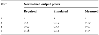
Table 2. 1 → 4 unequal power divider design parameters.
It is important to keep in mind that there is no need for simulation to design the power divider; it is included here only to show the accuracy of the proposed method. However, simulation is a powerful tool that may be used to optimize its performance, e.g. bandwidth.
The measured and simulated power law is included in Table 1. Such results fulfill the required power law fairly well. A comparison between the measurements and the results issued from the electromagnetic simulator Ansoft HFSS is presented in Fig. 11. Measured input return losses are better than 15 dB over roughly 16% bandwidth. Despite the differences when comparing the measured and simulated S11 over the frequency band, the power divider is still matched in the band of interest.
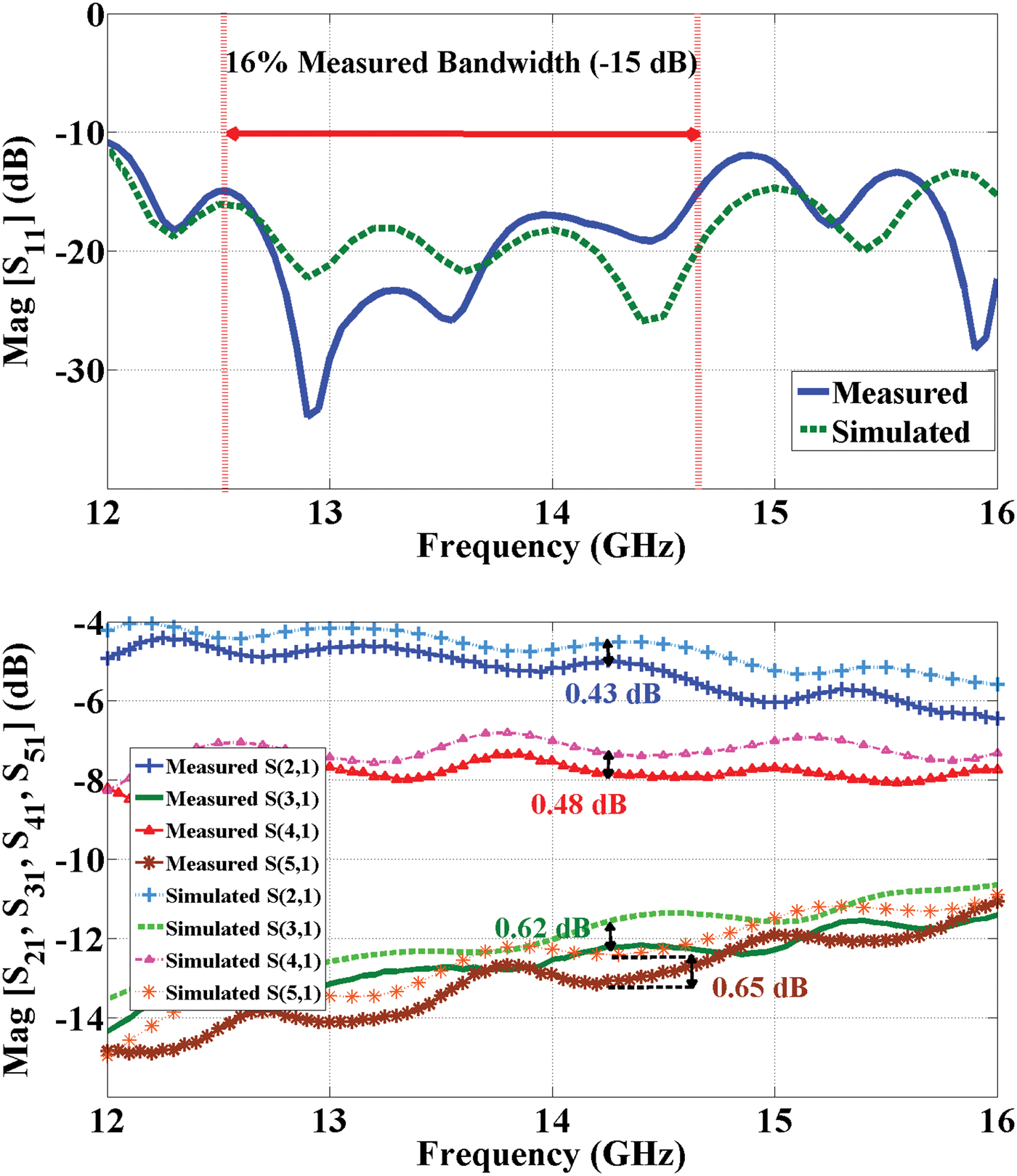
Fig. 11. Measured and simulated reflection (top) and transmission (bottom) S-parameters of the power divider depicted in Fig. 10.
Regarding transmission characteristics, good agreement is observed between the simulations and the whole measured bandwidth. The difference between the simulated and measured transmission coefficients is not the same for each output port. The explanation for this is that the input port shifting, performed for phase compensation, is different for the three Tee-junctions. Such a procedure leads to different path lengths from the input port P1 to the output ports P2, P3, P4, and P5. As the connector losses are only 0.1 dB, the remaining power level differences may be explained by two different factors. First, the substrate tangent loss is not specified by the manufacturer for the frequency band of interest; it was set to 3.35 × 10⁻³, which corresponds to 10 GHz. Second, the through vias were simulated as if they were totally filled by pure copper; however, they were actually metalized by a modified electrolytic copper deposition process.
The phase of the measured output signals are plotted at the top of Fig. 12. The four signals are phase-balanced, which demonstrates the accuracy of the proposed phase compensation method.

Fig. 12. Measured phase of the transmission S-parameters (top) and isolation coefficients between the output ports of the power divider depicted in Fig. 10.
The isolation between the output ports is also shown in Fig. 12. The low isolation levels achieved were expected due to the fact that no resistors were used between the Tee-junctions output ports. If the targeted application requires significant isolation levels, resistive elements have to be included and the Tee-junctions are considerably modified. A possible way to do this is by using Half Mode Substrate Integrated waveguides (HMSIW) as presented in [Reference Eom and Lee18]; however, this technique has the disadvantage of non-negligible radiation from the open ends of the HMSIW.
As previously explained, this methodology is scalable and all the parameters are referred to the guided wavelength. In consequence, it is applicable to any type of substrate. To validate this, other Tee-junctions were successfully designed using 0.254 mm thick substrate RO5880 (ɛ r = 2.2).
D) Discussion on the Tee-junction bandwidth
The Tee-junction bandwidth may be limited by two different factors: input matching and ΔOut variations. Regarding the first one, the structure is considered to be matched when the reflection coefficient S 11 is lower or equal to −18 dB. According to the simulations run during the curve generation process, the minimum input matching bandwidth is 28 and 15% for the low and high power split ratio cases, respectively. However, after measuring several implemented Tee-junctions, the bandwidths for which the input matching is guaranteed are 15% for 0 dB ≤ ΔOut ≤ 3 dB and 12% for 3 dB < ΔOut ≤ 9 dB.
The second factor that may limit the Tee-junction bandwidth is the transmission coefficients variation. Such variation affects the resulting ΔOut and the required power difference between the output ports is not longer achieved. The bandwidth evaluation is done by limiting the ΔOut variations to ±10% of its design value. Table 3 summarizes the simulated and measured results for some implementations at three different central frequencies and for three different power division ratios.
Table 3. Tee-junction bandwidth limited by the transmission coefficient variations.
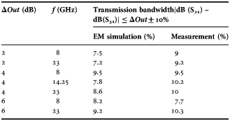
The results provided in this section show that the actual limiting factor when evaluating the bandwidth of the proposed structure is the variation in the transmission coefficients and not the input matching.
Finally, it is important to notice that the bandwidth results provided in this section were evaluated by using a particular criterion (ΔOut ± 10%) and it is the final application which really determines the required performance. In any case, the parameters recommended by the proposed methodology are a convenient starting point for the necessary optimization procedures.
V. CONCLUSION
A simple procedure to implement unequal power division through Tee-junctions in SIW technology has been presented. A set of curves was generated to easily determine the junction parameters to obtain the desired power ratio. A wide-range of split-power ratios, going from 1:1 to 1:8 are achievable. The phase-balance on the output signals is attained by shifting the Tee-junction input port. The procedure was illustrated by three examples at different frequency bands. One of such implemented examples presents the guidelines for the design of 1 → 2N unequal power dividers using Tee-junctions as a fundamental block. The measured results are in good agreement with the design criteria.
For the Tee-junctions, the input matching is guaranteed to be better than 18 dB over more than 12% bandwidth. The variation of the power difference between the output ports is lower than 10% over at least 7% bandwidth around the central frequency. Since the recommended values for all of the parameters are related to the guided wavelength, no simulation is required to complete the design. However, simulation is a powerful tool that may be used to optimize the design parameters from the starting values deduced from the graphical procedure for improving the performances e.g. bandwidth and input matching.
ACKNOWLEDGEMENT
This work is part of the studies developed for the AMORCE project, which is supported by the ANR.
 Soraya Contreras received the BSc. degree in electronic engineering from Universidad Distrital, Bogota, Colombia. In 2011, she received the MSc. degree in telecommunications and electronic engineering from Télécom Bretagne, Brest, France where she is currently pursuing the Ph.D. degree in Microwaves. Her current research interests include power distribution systems, BFN for phased arrays antennas, and power amplifier characterization.
 Alain Peden is a Professor at Telecom Bretagne, a graduate engineering school in Brest, France. He received his Ph.D. degree in Microwave Electronics from the University of Bretagne Occidentale, Brest, in 1991. From 1986 to 1988, he worked on design of low noise and power MMIC amplifiers at Thomson Hybrides et Microondes, Orsay, France. In 1991, he joined Telecom Bretagne and the LEST laboratory in Brest, where his research activities focused mainly on load-pull characterization of transistors in the Ka band and on design of quasi-optical amplifiers. Since 2003, his research activities, within the Lab-STICC (Laboratoire en Sciences et Techniques de l'Information, de la Communication et de la Connaissance) in Brest, have been dealing with millimeter wave applications, such as power combining techniques for solid state power amplifiers and automotive radar in the W band.


