


I. INTRODUCTION
A new method for the determination of film layers deposited onto Si single-crystal wafers has been developed. The method provides a measurement in that the thickness is determined with the only parameters being the following: the X-ray mass attenuation coefficients for Cu K α radiation, the film composition, film density, and a possible film morphology factor appropriate only for films that are not expected to exhibit full X-ray densities. The thickness measurements are nondestructive and can be performed in approximately 10 min including substrate alignment procedures. The principal application has been the measurement of SmCo based film thicknesses sputter deposited as hard permanent magnet films, and the thickness of pure Co films deposited by sputtering, onto Si (100) semiconductor wafers. It is shown that the dominant Si (400) reflection as well as a functional Si (200) reflection can be used for the thickness measurements. The SmCo based films had a nominal composition of Sm0.13Co0.58Fe0.20Cu0.07Zr0.02 (Hegde et al., Reference Hegde, Qian, Ahn and Cadieu1996). This composition for bulk magnets corresponds to that normally designated as SmCo 2–17 magnets (Parker, Reference Parker1990). When films are directly crystallized onto heated substrates with this composition it has been extensively shown that the films can be formed as a single-phase deposit with the TbCu7-type structure (Cadieu Reference Cadieu, M. and Vossen1992, Reference Cadieu, J. D. and Francombe2000). The advantages of this phase for film applications are twofold. One is that the films can be crystallized as highly textured deposits with the crystallite c-axes in general randomly splayed onto the film plane, and the second is that the films being single phase are insensitive to subsequent heat treatments. For film magnet applications this last point is important since it allows the films to be used directly as sputtered for applications requiring film magnetic biasing or as magnetic attractors (Cheng et al., Reference Cheng, Rumpler, Perkins, Zahn, Fonstad, Cramer, Zuneska and Cadieu2009). This method uses measurements of the attenuation of Si single-crystal diffraction lines by film layers deposited onto the Si wafers. Generally X-ray diffraction studies are done with a broad line focus source and then relative diffraction line intensities are recorded for comparison to either known or expected diffraction line intensities. In this new method a small point focus incident X-ray beam is utilized so that the diffracted intensities of certain single-crystal reflections are measured with and without the overlying film layers. An adjustable crossed slit collimator has been used so that the size of the irradiated region can be varied. It recently came to our attention that previously a similar approach had been used to measure the thickness of broad area films on single-crystal GaAs substrates (Chaudhuri and Shah, Reference Chaudhuri and Shah1990). A principle advantage for the use of single-crystal Si diffraction lines is that the count rate can be very high so that useful measurements can be accomplished in measurement times of approximately 2 min or less. In these studies a four-axis research diffractometer was used that allows quick substrate alignment to optimize the intensity from a desired single-crystal reflection. The thickness of the film layers can then be calculated from measured intensity ratios with and without film layers, the density, and X-ray mass attenuation coefficients for the compositions of the elements in the film layers. For the case of columnar or composite films, an additional factor has been introduced that is a measurement of either the volume void structure of the films or of the relative weighting of the composite phases.
The X-ray attenuation thickness measurement method has at least four advantages over the X-ray reflectivity for the measurement of film thicknesses on semiconductor substrates. One is that the range of thicknesses that can be measured is extended to at least several microns. Another is that the semiconductor surface can be rough. It is generally not feasible to do X-ray reflectivity measurements for films on even seemingly smooth glass substrates. A third is that this method can be done quickly with relatively inexpensive equipment. A fourth is that it can be adapted to the in situ measurement of the film thickness during film growth. In this regard it is similar to ellipsometry but is more suitable for monitoring the growth of thick metal films which are usually composed of materials that exhibit relatively high X-ray attenuation coefficients. The X-ray attenuation method can be useful not only for magnetic films deposited on Si thickness measurements, but also for the thickness measurement of foils just affixed to a substrate as is shown for the case of a Ni foil. The use of X-ray attenuation to measure a film morphology factor, a variable beam probe size, the possible use of functional not normally allowed reflections, and simple applications to measure the thickness of free standing foils are new applications of the film thickness measurement method.
II. EXPERIMENTAL
A Panalytical Materials Research diffractometer with a Cu X-ray tube operated in the point focus mode with a crossed slits collimator was used to record diffraction line intensities from Si semiconductor wafers with and without overlying film layers. A rocking curve receiver slit was used for the diffracted beam. This combination gave relatively low resolution which made it easier to compare net peak heights for different film layer thicknesses. With this arrangement diffracted beam height intensities of approximately 3×10⁵ cps are obtained for Si (100) wafers at the (400) diffraction line. A lower intensity reflection is also available at the position of the Si (200) diffraction line, even though that reflection is not allowed by the structure factor. This reflection will be referred to as a functional Si (200). This functional Si (200) reflection exhibits a moderate intensity, of about 30 000 versus 300 000 cps for the Si (400) at a lower 2θ value which may make it useful if the accessible 2θ is restricted. For Si (111) wafers a strong reflection is obtained at the (111) reflection of approximately 3×10⁵ cps, and then a weaker line is observed at the (333), and then weaker yet at the (222) reflection. For either wafer type the tube voltage is set to 45 kV and then the tube current limited to a value so that detector counts are limited to <3.5×10⁵ cps to avoid flooding the detector. For Si (100) wafers tube parameters of 45 kV and 30 mA were used. The crossed slits have been usually set to 1 mm×1 mm which at 69.129° of the Si (400) reflection results in an irradiated sample area measuring about 1.5×1.5 mm2. A smaller beam size could be used to scan patterned film regions, but we have not found it useful for the films of interest.
The method has been tested mainly for films deposited on Si (100) semiconductor wafers. The wafers used have a native oxide layer and no attempt has been made to remove the oxide layer which is normally about 1.5 nm thick, as measured by X-ray reflectivity, and is believed inconsequential for these thickness measurements. Base Si (400) intensities have been obtained in a number of ways. One is to mask part of the Si before deposition so that an exposed Si substrate region is available for comparison intensities. A second is to etch away part of the film so that a region of Si is exposed. A third is to use similar uncoated substrates. A fourth method is to use the back of the Si wafer for comparison intensity. Surprisingly the wafer polished and unpolished sides can give Si(400) intensities that are statistically indistinguishable. The Si wafer pieces are aligned by setting the 2θ angle to the value expected from the Bragg equation and
TABLE I. The mass attenuation coefficients for Cu K α radiation and densities used for thickness calculations are indicated.
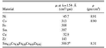
a Computed as linear combination.
then the samples are rotated about the ϕ-axis to the position of the maximum count rate. A scan over a 1° range in 2θ is made in the usual 2θ-ω mode.
The basic equation for the X-ray attenuation takes into account the double attenuation as the X-rays pass first into the film and then exit back through the overlying film
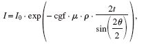
where μ is the mass attenuation coefficient; ρ is the density; t is the film thickness; and cgf is a columnar growth factor. The cgf for Co and Ni films has been set to 1.00. For Si (400), 2θ=69.129°. The general form of this equation is discussed in Azaroff (Reference Azaroff1968) as applied to reflections from single crystals. Modifications have been made here to include the attenuation caused by a film deposited on top of a single-crystal substrate. The parameters used are shown in Table I. To obtain the thicknesses of the Ni and Co films there are no adjustable parameters.
III. RESULTS AND DISCUSSION
Figure 1 shows the diffraction count rates for several different films. The low resolution optics do not resolve Cu K α 1 and Cu K α 2 contributions, but do make it easier to

Figure 1. (Color online) Representative count rates for the Si (400) reflection are indicated with and without deposited films. A Cu X-ray tube with crossed slits collimator was used to obtain these count rates. Respective net peak height intensities are indicated.
TABLE II. Ni foil thickness determined from X-ray attenuation of the functional Si (200) and Si (400) reflections for differing placements of the Ni foil are indicated. The functional Si (200) data were collected without a tube Ni β filter to raise the base counts to over 30 000 cps.
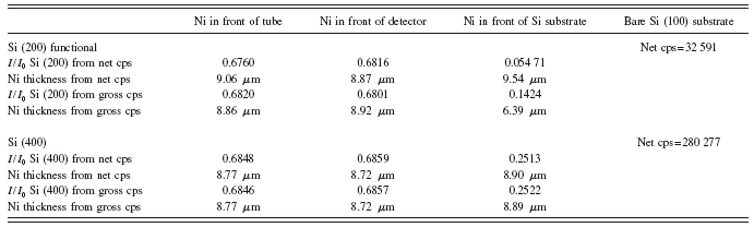
compare net peak heights. The Cu K α 2 contribution skews the peak profiles to the high-angle side. Most of the films investigated have been deposited onto the Si wafers at temperatures less that 450 °C and for these conditions the reflection properties of the Si wafer are unchanged by the film depositions. In general a bare Si (400) scan has been obtained for each individual film. In Figure 1 the bare Si (400) corresponds to the thinnest Co film illustrated. A proof of method has been obtained by determining the thickness of a Ni foil that has been placed sequentially in front of and perpendicular to the X-ray beam, in front of the detector and perpendicular to the X-ray beam, and affixed to the Si wafer surface. Table II shows the Si (400) and functional Si (200) intensity ratios as determined from the net peak height intensities which are corrected for background levels, from the gross peak intensities, and the calculated film thicknesses for the three Ni placement positions. The best agreement is achieved by using the net peak intensities particularly for the functional Si (200) reflection where the count rate is substantially lower than at the Si (400) reflection. The net peak height intensities are found simply from the Panalytical “peak mode” of the scan display window. The nickel foil thickness measured from the foil mass and area dimensions was 8.9±0.3 μm. This value agrees closely with the values determined from the X-ray attenuation.
A series of Co films have been deposited onto bare Si (100) wafer pieces under the same sputtering conditions with only the length of sputtering times varied. For the Co thickness range studied no boundary layer was necessary to allow the adhesion of the thin Co films to the Si wafers. The Co films were magnetron sputtered under 40 mTorr Ar with the wafers heated to 100 °C during the deposition. The Co film thicknesses have been measured by observing the intensity of the Si (400) diffraction reflection for Cu K α radiation. These results are indicated in Figure 2 and certain films have also been measured by a profilometer courtesy of the T. J. Watson IBM Research Center. In this case it should be noted that the thickness measurements by both methods closely agree within at least 5%.
Various SmCo based films have been deposited onto principally Si (100) wafer pieces. Films have been deposited onto both cold (room temperature) and heated substrates so that the SmCo based films are directly crystallized and exhibit specific growth morphologies. For the SmCo based films a thin boundary layer of Ta was deposited as an adhesion layer onto the Si (100) wafer pieces in a separate sputtering system. The Ta boundary layer was sputter deposited in a separate system and was about 30 nm thick. This Ta layer is very thin compared to the SmCo film thickness and has been ignored in calculating the several micron SmCo film thicknesses. The Co films were sputter deposited onto the Si wafers without the use of any adhesion layer since it was of interest to measure the thicknesses of Co films as thin as 10 nm. The Co and the cold deposited SmCo based films exhibit very small grains and are expected to exhibit bulk densities close to the expected X-ray densities.
The SmCo based films deposited cold are at first amorphous and can then subsequently in situ be heated to 500 °C to cause crystallization. The grain size in this case has been previously measured to be about 40 nm. The SmCo based films that were directly crystallized onto heated substrates (T≥350 °C) exhibit textured grains with the crystallite c-axes aligned onto the substrate plane. These grains also exhibit columnar growth morphology with random voids between the grains. Figure 3 shows SEM pictures for representative SmCo based films that were deposited onto a cold substrate to be first amorphous and were then subsequently crystallized in situ, on the left, and for SmCo based films that

Figure 2. (Color online) Co film thicknesses, as measured by Si (400) reflection attenuation, for films deposited for differing deposition times are indicated by squares. The thicknesses of certain Co films were measured by a profilometer at IBM.

Figure 3. The left panel shows the grain structure for a SmCo based film that was first made amorphous by sputter depositing onto a cold substrate which was then heated to crystallize the film. The right panel shows the surface of a highly textured SmCo based film that was directly crystallized by thermalized sputtering onto a heated substrate.
were deposited by selectively thermalized sputtering onto a heated substrate so that the crystallite c-axes are randomly splayed onto the substrate plane. The film was almost totally (200) textured of the TbCu7-type structure, with some admixture of the (110) orientation. Films of this type can exhibit high magnetic energy densities of the order of 15 MGOe. The directly crystallized films exhibit a mosaic of irregular columnar growth. Previously it has been shown that by sputter process control such films can be grown to a thickness of at least 120 μm with same texturing and growth morphology being maintained. A cut at any thickness then has a similar cross section of film and void regions as depicted in the film surface picture of Figure 3. Such films are a special case of composite films where one component is simply space voids of very low density.
The films directly synthesized as textured films with the c-axes aligned onto the substrate plane exhibit a columnar growth with voids as illustrated in the left panel of Figure 3. A columnar growth factor, cfg, has been introduced which effectively acts to lower the average density and X-ray attenuation. Figure 4 shows film thickness measurements for two directly crystallized SmCo based films, TD209 and TD410, and from a SmCo based film that was deposited onto

Figure 4. (Color online) The expected variations in the film thickness are shown for two relatively thick SmCo based films that were highly textured with the crystallites aligned onto the film plane. The corresponding horizontal lines indicate the respective film thicknesses measured by a profilometer. The cgf factor is found when these two curves intersect.
a cold substrate, TD720, as measured from the attenuation of the Si (400) diffraction reflection. The cold film was left amorphous and should be strain free and is expected to exhibit full density. Films TD209 and TD720 were deposited under the same sputtering gas pressure and length of sputtering time except that the substrate for TD209 was heated to 400 °C during deposition to promote direct crystallization upon deposition. No fundamental distinction between the X-ray attenuation observed at the functional Si (200) and Si (400) diffraction angles has been observed. We have mainly used the intensity ratio for the Si (400) reflection because the count rates are much higher than at the functional Si (200) reflection. For the two film samples shown in Figure 4 the film thickness measured by the X-ray attenuation method gave thicknesses of 2.21 and 3.27 μm, and the profilometer gave 2.37 and 3.54, respectively. These measurements are brought into agreement at a cgf of 0.94±0.02. In measuring the thickness of similar highly textured SmCo based films the thicknesses measured by X-ray attenuation can be recalibrated to the profilometer measurement values by the use of a cgf of 0.94. The cold deposited film, here identified as TD720, with a 1 s dwell time, exhibited for the bare Si a net peak height of 225 635±475 cps and the net peak height for the SmCo film the film attenuated peak was 12 799±113 cps. Based on the counting statistics this translates to a measured thickness of 3.26±0.01 μm. Certain additional systematic errors because of errors in the mass attenuation coefficients and expected full densities would cause equivalent film thickness measurement shifts for all three films. The thicknesses of films TD209 and TD720 measured from the X-ray attenuation are the same. The thickness of TD209 is brought into agreement with the profilometer thickness measurements for that film with the use of a cgf factor of 0.94±0.02 to account for the highly textured columnar grain growth of film TD209. For the Co films measured which are expected to be fully dense the cgf factor is simply 1 and the X-ray and profilometer thickness measurements agree within the tolerances.
Certain thinner SmCo based films that exhibited stress cracking exhibited anomalously thin values when the thickness was measured by the X-ray attenuation method. Apparently in this case the stress cracked surface acted to expose the underlying Si surface which then resulted in less attenuation being recorded. A Peltier cooled solid state X-ray fluorescence detector was placed in close proximity to the films so that the relative amounts of Sm, Fe, and Co in the films could be measured. Such an X-ray fluorescence trace is shown in Figure 5. There was little variation in the film compositions for the films reported on in this paper. Variations in SmCo based film compositions due to differences in sputtering parameters and as measured by X-ray fluorescence will be discussed in a subsequent paper.
IV. CONCLUSION
It has been demonstrated that thickness measurements can be made nondestructively for Co and SmCo based films deposited onto single-crystal Si (100) semiconductor wafers. A complete thickness measurement can be made in approximately 10 min which includes the time required to align the film and substrate. The accuracy of the thickness measurements

Figure 5. (Color online) X-ray fluorescence counts for the thicker film shown in Figure 4 is shown as collected by a Peltier cooled solid state X-ray detector.
depends on the effective mass attenuation coefficient of the film material. For the materials considered, the thicknesses determined by the X-ray attenuation method agree within at least several percent to the values determined by other methods. In some applications this technique could be used for in situ film growth monitoring. It should be noted that it is not necessary to scan the diffracted angle so that the attenuation measurement system could be very simple in design. For such applications the low diffraction angle for the functional Si (200) reflection may be advantageous. For Co films thicknesses down to tens of nanometers to hundreds of nanometers can be measured with the only input parameters being the mass attenuation coefficient for Co at λ=0.154 nm and the density of Co. The Co film thickness measurements agree with the profilometer measurements within at least 10% from 50 to 350 nm. Measurements of the 8.9 μm thick free standing Ni foil just affixed to a Si substrate agreed within about 2% to the thickness that could be measured with a micrometer. SmCo based film thicknesses up to at least 5 μm could be measured. For the case of SmCo based films exhibiting a columnar growth morphology an additional columnar growth factor, cgf, has been introduced which experimentally has been shown to have a value of about 0.94. The X-ray attenuation thickness measurements of the SmCo based films corrected with the cgf factor are within several percent of the profilometer measurements.
ACKNOWLEDGMENTS
This research was supported in part by the PSC-CUNY FRAP. Discussions with C. V. Jahnes and S. Hegde are gratefully acknowledged.


