I. INTRODUCTION
The square kilometre array (SKA) [Reference Dewdney, Hall, Schilizzi and Lazio1] will be a next generation, ground-based, radio telescope with an aperture of up to a million square meters. The SKA will consist of an array of coherently connected antennae, spread over an area of about 3000 km in extent. The SKA will provide unsurpassed sensitivity and multiple beams of very high angular resolution in the radio frequency (RF) window from 70 MHz to 30 GHz. The SKA will be operational below 10 GHz by 2022.
The SKA will be built to further the understanding of the most important phenomena in the Universe. To help define the requirements of the SKA, consideration has been focused on five Key Science Projects (KSPs) [Reference Carilli and Rawlings2]. Each KSP represents an unanswered question in fundamental physics or astrophysics and is either unique to the SKA or where the SKA plays a key role. The SKA science impact will be widely felt in cosmology, physics, astronomy and astrobiology.
The technical specifications [Reference Schilizzi3] are derived from the KSPs, but are constrained by other aspects of design, such as feasibility and cost. A key figure of merit is the survey speed, a measure of how fast a given fraction of the sky can be mapped out with a given sensitivity. The survey speed is defined as (A eff/T sys)2 Ω, the product of the square of the instantaneous telescope sensitivity, A eff, divided by the system temperature, T sys, and the instantaneous field of view (FoV), Ω.
The construction of the SKA is a complex challenge with no unique solution, with many different technological solutions selected and integrated into the final instrument. The coverage of the wide bandwidth of the SKA cannot be managed by a single antenna technology when the sensitivity and efficiency requirements of the SKA are also considered. The construction of the SKA will be determined by the results of ongoing pathfinder projects and design studies [Reference Greenwood4].
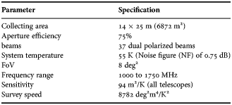
One such project, aperture tile in focus (APERTIF), will be built to demonstrate that phased array feed (PAF) technologies are sufficiently mature to be a viable concept for SKA by improving the survey speed of reflector telescopes while preserving the sensitivity required to adhere to the specifications of SKA [Reference van Cappellen and Bakker5]. PAF is a novel method to form multiple beams on the sky with a reflector antenna. The specifications of APERTIF are defined in Table 1.
Table 1. APERTIF Specifications.

By replacing the current single receiver of each Westerbork synthesis radio telescope (WSRT) dish by an array of receivers, the survey speed of the WSRT is enhanced by a factor 20. The PAF will reduce the sensitivity of a single beam observation, but in terms of survey speed this is more than compensated by the 37 times larger FoV. The front end consists of a dual polarized antenna array that is mounted in the prime focus of the WSRT reflector.
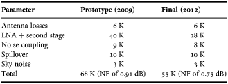
Each element of the antenna array connects to a low noise amplifier (LNA) via a balun. To minimize the conductive and dielectric losses, the balun and the LNA are integrated on a single low-loss printed circuit board (PCB) [Reference Arts, Ivashina, Iupikov, Bakker and van den Brink6]. As the size of the PAF precludes cryogenic cooling as an effective method to minimize noise, there is an increase in T sys. The LNA is a major contributor to T sys, with an LNA noise temperature of 25 K (NF of 0.36 dB) required to obtain the desired T sys [Reference bij de Vaate, Bakker, Woestenburg, Witvers, Kant and van Cappellen7], as defined in Table 2.
Table 2. System temperature contributions.
While there are a few institutes investigating various LNA technologies and topologies that could potentially meet these requirements, none yet meet all of the specifications [Reference Bhaumik and George8]. While the noise temperature has been met by [Reference Belostotski and Haslett9], the gain is low and the LNA is not available as a component off the shelf (COTS). Most of the potential solutions are based on custom made monolithic microwave integrated circuit (MMIC) chips, which involves a costly and time consuming design and manufacturing process.
In this paper, a compact, microstrip, two-stage, room temperature, single-ended LNA is designed, using commercial components to meet the noise temperature requirements of APERTIF. The design procedure is detailed from component amplifier selection to completed circuit for various options implementing source inductive feedback.
II. DESIGN
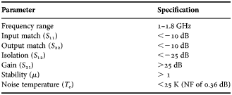
The specifications of the LNA are defined in Table 3. The size is minimized to remain within the physical constraints of the feed and to minimize the dielectric losses. Two stages are used to maximize the gain to reduce the effect of later stages on the system temperature. It is a room temperature device due to the difficulty in economically cooling the large feed. It has a 50 Ω single-ended input to connect to the balun at the output of the tapered slot antenna element.
Table 3. LNA specification.

The LNA is a microstrip circuit, designed using component amplifiers, which are soldered onto a low loss substrate, along with the chip components required to match and bias the component amplifiers, as depicted in Fig. 1. The number of components used is limited to minimize the noise, therefore components are required to perform both power and noise matching simultaneously. However, a compromise is required, as these two methods are not complementary.

Fig. 1. Diagram of LNA.
The noise temperature, T e, of an LNA as a function of its set of noise parameters is given by [Reference Woestenburg10]
 $$T_e=T_{min}+{4R_nT_0 \over Z_0} {{\vert \Gamma_s-\Gamma_{opt}\vert ^2}\over {\vert 1+\Gamma_{opt}\vert ^2\lpar 1-\vert \Gamma_s\vert ^2\rpar }}\comma \;$$
where T min is the minimum noise temperature, R n is the noise resistance, T 0 is the IEEE defined standard temperature of 290 K, Z 0 is the characteristic impedance, Γs is the source reflection coefficient and Γopt is the optimal source reflection coefficient that results in minimum noise temperature. In this case, Z 0 is 50 Ω to match the balun at the output of the antenna element.
In power matching, the source impedance is matched to Z 0, thereby minimizing Γs. From (1), this will raise T e above T min proportional to the value of Γopt. Conversely, in noise matching, Γs is matched to T opt, thereby minimizing T e. However, from (1), this will lead to a power mismatch proportional to the value of Γopt. Therefore, the LNA design is simplified by making power and noise matching complementary in making use of component amplifiers with low Γopt values.
A) Component amplifier
In this paper, the LNA is designed using COTS. This is significantly cheaper and faster than designing and manufacturing an MMIC. However, in doing this, the design procedure of the component amplifiers is relinquished to the manufacturer of these components. With regard to the component amplifier, the only decision left to the designer of the LNA is the choice thereof. After a cursory study of various manufacturers, based on noise parameters, two potential component amplifiers were selected.
A potential component amplifier for this design is the Avago MGA-633P8 package, with its noise parameters defined in Table 4. This package is well noise matched and well power matched. Therefore, connecting this package to the 50 Ω balun will have little effect on the noise temperature, thereby simplifying the design. However, as the minimum noise temperature exceeds the noise temperature specification, this package is excluded as an option.
Table 4. Avago package noise parameters.
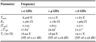
Another candidate is the Ommic CGY2106XHV, with its noise parameters defined in Table 5. This package is chosen for its exceptionally low minimum noise temperature. However, the design is complicated by the high Γopt values. Added to this, inductance is required between the source pad of the package and the ground plane of the PCB to increase the input resistance in order to improve the input power match.
Table 5. Ommic package noise parameters.

The effect of connecting the two packages to a 50 Ω input load, simulated in AWR Microwave Office (AWR MWO), shows why the Ommic package is preferred, with the results depicted in Fig. 2. As the Avago package is well power matched, the low Γopt value has little effect on the noise temperature. Conversely, as the Ommic package is poorly power matched, the high Γopt value has a significant effect on the noise temperature. However, due to the exceptionally low T min of the Ommic package, the resulting T e meets the design requirement.

Fig. 2. Component amplifier noise temperature.
The power parameters of the Ommic package are defined in Table 6. With two stages, this package will meet the gain and isolation specifications, while the input match, output match and stability specifications are exceeded. However, these specifications can be met by careful selection of components for the power and noise biasing, resulting in matching networks at the input and output ports that improve the power match without exceeding the noise temperature specification.
Table 6. Component amplifier power parameters.
A disadvantage of the Ommic package is that the source and ground pads of the package are internally connected to each other, which complicates the application of the source inductive feedback as the ground pad of the package cannot be directly connected to the ground plane of the PCB. Therefore, a number of methods of inserting inductance between the source pad of the package and the ground plane of the PCB are compared, with the emphasis on a mass producible design.
The design process that follows is one of progressive insight, with improvements based more on intuition and experience than the literature study. While the first method is based on a previous work [Reference Weinreb, Bardin and Mani11], it is not a reliable method, but more of a quick test of the theory that the insertion of the inductance between the source pad of the package and the ground plane of the PCB would improve the input match. The other methods are just practical attempts to make this process mass producible.
1) OPTION ONE
The package is flipped around and glued to the top layer of the PCB, as depicted in Fig. 3. As the package pads are raised above the level of the top layer of the PCB, physical connections are required between the package and the PCB layout. These connections are made with bonding wires. However, these connections are fragile, requiring some form of conformal coating to provide protection, and cannot be repeated accurately.

Fig. 3. Diagram of glued package (side view).
2) OPTION TWO
The package is flipped around and embedded within a square hole cut into the PCB, with a second PCB glued to the bottom layer for support, as depicted in Fig. 4. With a PCB equivalent in height to the package, the package pads are level with the top layer of the PCB, with chip components used to make the connections between the package and the PCB layout. However, the manufacturing process is a limiting factor in this design.

Fig. 4. Diagram of embedded package (side view).
3) OPTION THREE
The package is directly connected to the PCB layout, but with circuitry etched on the bottom layer of the PCB to indirectly connect the source pad of the package to the ground plane of the PCB, as depicted in Fig. 5. The combination of etching and chip components is used to create the inductance between the source pad of the package and the ground plane of the PCB. However, intensive computational power is required to model the bottom layer of the PCB.

Fig. 5. Diagram of bottom layer etched package (top view).
4) OPTIONS FOUR AND FIVE
The package is directly connected to the PCB layout, but with the footprint of the source pad of the package only indirectly connected to the ground plane of the PCB, as depicted in Fig. 6. Two options for creating the inductance between the source pad of the package and the ground plane of the PCB are attempted. One, using only etching, with long, thin lines required for the first stage. Two, using a combination of etching and chip components.

Fig. 6. Diagram of top layer etched package (top view).
The substrate is made from low loss Rogers RO4003 dielectric material of 0.8128 mm thickness, with copper cladding of 0.017 mm thickness. The relative permittivity, ɛr, is 3.38, the dissipation factor, tand, is 0.0027 and the conductivity, σ, is 5.88 × 10⁷ S/m. The stability of the relative permittivity over the temperature range of −50 to 150 °C and at frequencies up to 10 GHz, along with the low loss, makes it an ideal substrate for low noise broadband applications.
The chip components are of size 0603, apart from the 47 µF capacitors of the direct current (DC) circuitry that are of size 1206. The RF circuitry uses muRata GQM capacitors, LQG18H inductors, and LQW18A inductors. The DC circuitry uses muRata GRM capacitors. The LQW18A inductors are preferred due to their lower resistances, higher Q factors, and higher self-resonant frequencies, with the LQG18H inductors used due to the lower inductance values available with this series.
B) Amplifier
To minimize the LNA size, the number of components is minimized by combining the biasing and matching networks, as depicted in Fig. 7. From the bias setting data supplied by the manufacturer, both stages are biased for minimum noise temperature, with a drain voltage of 2.5 V, a drain current of 50 mA, and a gate voltage of −0.5 V. Where possible, resistors are avoided due to their noise contribution. However, resistors are required to improve stability and to prevent gate current.

Fig. 7. Circuit of LNA.
1) OPTION ONE
The two stages have equivalent circuits, apart from the second stage's negative RLC feedback loop, as depicted in Fig. 8. Due to the fragile nature of the bonding wires, these connections are covered by conformal coating to provide protection. The application of these connections and their coating is time consuming and cannot be applied accurately. Therefore, this method is excluded as an option.

Fig. 8. Photograph of glued package (top view).
2) OPTION TWO
The two stages have equivalent circuits, apart from the second stage negative RLC feedback loop, as depicted in Fig. 9. The RLC feedback loop is deemed unnecessary, and is excluded from further designs. The connections between the package and the PCB circuitry are stable and repeatable. However, the manufacture of the square hole for the package and the adhesion of the second PCB is time consuming. Therefore, this method is excluded as an option.

Fig. 9. Photograph of embedded package (top view).
3) OPTION THREE
The two stages have equivalent circuits, apart from the connection between the ground pad of the package and the ground plane of the PCB, as depicted in Fig. 10. As the first stage requires inductance between the source pad and the ground plane, inductors are used. As the second stage does not, resistors are used. The electromagnetic (EM) solvers are unable to correctly predict the behavior of the bottom layer of the PCB. Therefore, this method is excluded as an option.

Fig. 10. Photograph of bottom layer etched package (top view).
4) OPTION FOUR
The two stages have equivalent circuits, apart from the inductance at the input pad of the first stage and the etching between the source pad of the first stage and ground plane, as depicted in Fig. 11. As the package is directly connected to the PCB layout, chip components are not required. However, the etching used to create this extra inductance caused the LNA to oscillate around 8 GHz. Therefore, this method is excluded as an option.

Fig. 11. Photograph of top layer etched package (top view).
5) OPTION FIVE
The two stages have equivalent circuits, apart from the inductance at the input pad of the first stage and the etching between the source pad of the first stage and ground plane, as depicted in Fig. 12. The combination of connecting the package directly to the PCB and the use of chip components to increase to inductance between the source pad of the first stage and the ground plane have created a stable and repeatable, easily manufacturable, LNA design.

Fig. 12. Photograph of top layer etched package revised (top view).
III. RESULTS
The LNA was designed in AWR MWO and verified in Agilent ADS. The design process for each option began with ideal components, with the circuitry first ignored, then implemented with standard microstrip models before finally being modeled with the EM solvers of AWR Axiem and Agilent Momentum. Due to the indirect connection between the source pad of the package and the ground plane of the PCB, the etched options required intensive EM modeling.
All five options were built, with the scattering and noise parameters measured on the Agilent N5242A PNA-X Network Analyser and the noise temperature measured on the Agilent N8975A Noise Figure Analyser. All the measurements were performed within a Faraday Cage to shield from RFI. As the fifth option gave the best results, with regard to the specifications and the manufacturing process, only its measurement and simulation results are discussed further in detail.
As current is required at the output stages, the resistors used in the output matching and biasing networks are of size 47 Ω, increasing the output voltages to 4.85 V. However, as no current is required at the input stages, resistors of size 100 kΩ are used, maintaining the input voltages at −0.5 V.
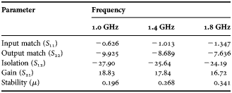
The LNA is well input matched, S 11 <−10 dB, and output matched, S 22 <−18 dB, up to 1.6 GHz, as depicted in Figs. 13 and 14. The simulations do not predict the measurements accurately due to the tolerance values of the chip components, resulting in a shift in frequency, and the non-standard grounding of the component amplifiers, resulting is a worse match.

Fig. 13. Amplifier input matching results.

Fig. 14. Amplifier output matching results.
The LNA is well isolated, S 12 <−42 dB, and has decent gain for a two-stage amplifier, S 21 > 34 dB, as depicted in Figs. 15 and 16. The discrepancy between the measurements and the simulations is due to the non-modeled effect of the non-standard grounding of the component amplifiers. However, this discrepancy is welcome as the higher the gain of the LNA the less the effect of later stages on the noise temperature.

Fig. 15. Amplifier isolation results.

Fig. 16. Amplifier gain results.
Boards were built to measure the effect of indirectly grounding the component amplifier packages of the two stages. When compared to simulated results there is an unexpected increase in the gain of 2.1 dB for the first stage and 2.3 dB for the second stage, as depicted in Fig. 17, which largely explains the discrepancy in the gain of the amplifier in Fig. 16.

Fig. 17. Indirect grounding results.
Low inductance values are required between the source pad of the package and the ground plane of the PCB. However, at these inductance values the tolerance value for the chip inductors is 0.3 nH, which is a variance of up to 25%, which has a marked effect on the simulated results of the input match, as depicted in Fig. 18. This is reduced by using higher valued inductors, which have lower variance values, in parallel.

Fig. 18. Chip component tolerance results for input match (S 11).
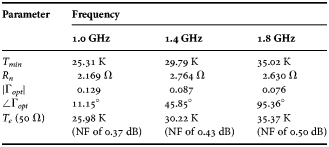
The LNA is unconditionally stable, μ > 1.1, as depicted in Fig. 19. As the μ factor is calculated from the scattering parameters, the measured stability differs from the simulated results. The noise temperature is 23.7 K (NF of 0.34 dB) on average, which while being 5.5 K (NF of 0.08 dB) higher on average than the simulated results, still meets the noise specification, as depicted in Fig. 20.

Fig. 19. Amplifier stability results.

Fig. 20. Amplifier noise temperature results.
The noise temperatures of a few of the options are compared in Fig. 21. The first and fourth options are omitted, due to their instability causing them to not properly function during the measurement process. On average, the fifth option is 9 K (NF of 0.13 dB) better than the second and the third options.

Fig. 21. Amplifier noise temperature results comparison.
No attempt is made to counter the 7.4 dB roll off of the gain of the LNA, as this would require additional components which would increase the noise temperature of the LNA. However, with a noise temperature of 23.7 K (NF of 0.34 dB) and a gain of 38.6 dB, any subsequent stage with gain correction would have a minimal effect on the system noise temperature.
IV. CONCLUSION
In this paper, a LNA is designed as a potential solution for APERTIF, a SKA Pathfinder Project. The desired noise temperature of 25 K (NF of 0.36 dB) is met over the 1.0–1.8 GHz band, with an input return loss better than 10 dB, an output return loss better than 10 dB, a gain better than 34 dB, isolation better than 42 dB, and unconditional stability.
To minimize the conductive and dielectric losses, the LNA is developed as a microstrip circuit and is matched to a single-ended 50 Ω input load so as to be integrated on a single low-loss PCB with the balun at the output of the tapered slot antenna elements of the PAF. The size of the LNA is compact enough to fit within the size restraints of the PAF.
Now that it is possible to insert inductance between the source pad of the package and the ground plane of the PCB using standard manufacturing techniques, the LNA is ready for implementation on a large scale. However, in order to be used in APERTIF, a filter is required between the first stage and the second stage, to avoid saturation by radio frequency interference (RFI) and to remove the gain slope. Also, the LNA still needs to be integrated with the other elements of the PAF onto a single substrate.
The LNA requires no cooling to obtain its noise temperature of 25 K (NF of 0.36 dB), necessary as the size of the PAF precludes cryogenic cooling as an effective method to minimize noise. The noise contribution of the LNA fits within the noise budget of APERTIF and provides sufficient gain to minimize the effect of later stages on the required system temperature of 55 K (NF of 0.75 dB).
The PAF of APERTIF contains 144 antenna elements, each connected to their own circuitry. The noise performance of the LNA being such that cryogenic cooling is not required to meet the system temperature specification, and due to the low cost of the Ommic packages, in the order of a few euros per package, the cost of the LNA is only a small fraction of the financial budget of APERTIF.
The LNA is designed using commercial components. As the source pad and ground pad of the component amplifier packages are connected to each other, various techniques are investigated to insert inductance between the source pad of the package and the ground plane of the PCB. The chosen design is able to do this using standard manufacturing techniques.
ACKNOWLEDGEMENTS
D.M.P.S. thanks NRF for funding this work and ASTRON for hosting him at their institute.
 David Smith received his BEng, M.Sc.Eng and Ph.D. in Electronic Engineering from Stellenbosch University in the period 2001 until 2010. From 2010 to 2011, he held a post doctoral position at Stellenbosch University working on a LNA for APERTIF, a SKA Pathfinder Project. Currently, he holds a post doctoral position at ASTRON working on the OLFAR Project.
 Laurens Bakker received his M.Sc. in Electrical Engineering from Twente University in 2001. From 2001 to 2006, he held a researcher position at Eindhoven University of Technology, working on high speed optical data transmission and analog optical communication. Currently, he is a system engineer working on APERTIF at ASTRON. His interests include communication systems, low noise systems, RF system design, and digital signal processing.
 Roel Witvers received his BsE from Hogeschool Enschede in 1997. Since 1997, he has been working at ASTRON at the R&D Department and worked mainly on LNAs. He specializes in the design of MMIC LNAs on GaAs and InP. He has worked on several demonstrators developed at ASTRON to prove the concept of PAF for use in radio astronomy. Currently, he is an instrument engineer working on uncooled LNAs for use in SKA.
 Bert Woestenburg received his degree in Microwave Engineering from Twente University in 1983. He has been involved in the design of LNAs and receiver systems, mainly for the WSRT, since the start of his professional career at ASTRON. Currently, he is the head of the RF & Low Noise Systems group at ASTRON. His interests lie in the design of LNAs and the noise characterization of aperture arrays and PAF systems.
 Keith Palmer received his BEng, BEng (Hons), M.Sc.Eng and Ph.D. degrees from Stellenbosch University in 1977, 1978, 1982 and 1997, respectively. Since 1978, he has been on the academic staff at Stellenbosch University, where he is currently an associate professor in the high frequency engineering group specializing in antenna theory and design with a focus on satellite, radar and wideband antennas.