


Introduction
The significance of lowpass filters (LPFs) in increasing the quality of communicating signals cannot be ignored as these blocks eliminate undesired frequencies. Hence, various geometries have been introduced [Reference Wang, Xu, Zhao, Guo and Wu1–Reference Afzali, Karkhanehchi and Karimi18] to attain desired frequency response properties such as steep transition band, acceptable stopband, and passband characteristics. Addressing these challenging features, in [Reference Wang, Xu, Zhao, Guo and Wu1], radial-shape resonators have been employed to obtain an LPF; however, the designed filter failed in attaining a steep skirt performance. Hairpin resonance cells have been considered as one of the popular structures as reported in [Reference Luo, Zhu and Sun2–Reference Velidi and Sanyal5]. For instance, in [Reference Luo, Zhu and Sun2], by using this unit, acceptable stopband characteristics have been achieved, although the circuit size and the cut-off sharpness are not satisfactory. Utilizing hairpin cell with radial patches is another LPF structure, which has been introduced in [Reference Wei, Wang, Liu and Shi3], but its stopband features are weak. Similar to [Reference Wei, Wang, Liu and Shi3], the proposed LPF in [Reference Li, Li and Mao4] employing stepped impedance hairpin resonator suffers from a narrow stopband. In [Reference Velidi and Sanyal5], an employment of coupled-line structure in hairpin cell has been described, even though applying shunt open-stubs to the conventional hairpin unit failed in creating a steep transition band. Applying a rat-race coupler to an LPF is another interesting technique, which has been implemented in [Reference Gomez-Garcia, Sanchez-Soriano, Sanchez Renedo, Torregrosa Penalva and Bronchalo6]. The main drawback of this approach is its very large circuit size. To implement an LPF with a novel design, a slotted-ground-plane resonator has been utilized in [Reference Wang and Lin7], although its in-band and out-band performances are not acceptable. In [Reference Wang, Cui and Zhang8], combining triangular and radial resonators has led to obtaining an LPF capable of suppressing the 16th harmonic response corresponded to a suppression level of 15 dB. Unfortunately, its slow roll-off rate has decreased the efficiency of this filter. To attain an LPF presenting an expanded rejection band, hairpin unit and semi-circle cells have been combined, in [Reference Wei, Chen, Shi, Huang and Wang9]. In [Reference Ma and Yeo10], modified radial structures have been adopted to achieve an LPF with desired rejection band properties. Nonetheless, the applied methods of designing each LPF in [Reference Wei, Chen, Shi, Huang and Wang9] and [Reference Ma and Yeo10] have failed in improving the steepness of the transition band. Reference [Reference Hayati, Abdipour and Abdipour11] introduces a LPF using triangular and polygonal resonant patches, although its in-band performance is not desired. The conducting metal etched off in specific shape from the ground plane or the so-called defected ground structure (DGS) can reduce out-of-band harmonics through creating high slow wave effect, as reported in [Reference Xiao, Sun and Li12–Reference Mandal, Mandal, Sanyal and Chakrabarty14]. Unfortunately, applying DGS to these filters makes them unusable on metal surfaces thanks to the etched resonators on the ground plane. Another method to improve the rejection band characteristics of an LPF is utilizing multimode resonators, which has been reported in [Reference Li, Zhang and Fan15]. In [Reference Jiang and Xu16], circular sectors and a pair of quadrants have been compounded to demonstrate a new LPF structure with remarkable stopband performance. By employing radial stub resonator and folded microstrip lines, another LPF has been proposed in [Reference Hayati, Amiri and Faramarzi17]. In [Reference Afzali, Karkhanehchi and Karimi18], an LPF adopting modified T-shaped and cursive transmission lines has been reported. In spite of introducing new configurations in [Reference Li, Zhang and Fan15–Reference Afzali, Karkhanehchi and Karimi18], each of them suffers from a weak frequency response performance in the transition band. In [Reference Li, Bao, Du and Wang19], to expand the stopband band width, an LPF capable of creating three transmission zeros (TZs) has been proposed, but the sharpness of the design is not satisfactory. Employing comb CMRC [Reference Zhang20] and using thin slots [Reference Wu, Tseng and Tu21] have been introduced in order to design LPFs with desired frequency responses. To achieve a steep roll-off rate in [Reference Velidi and Sanyal22], transmission line elements have been used to create an equiripple LPF response. In [Reference Cui, Wang and Zhang23], another LPF employing two different cells, i.e. triangular patch resonators and polygonal patch resonators to obtain an ultra-wide stopband, has been proposed. However, each of the proposed LPFs in [Reference Velidi and Sanyal22] and [Reference Cui, Wang and Zhang23] does not have a sharp transition band.
In this paper, two resonators which can be considered as the main resonance cells have been introduced. The first unit consists of a pair of modified T-shaped patches. Using these patches with extra parts can increase the degree of freedom in controlling the operating frequency. However, this resonator cannot create a sharp roll-off rate. Thus, the second resonance cell composing of four polygon patches is added to the first resonator to play a complementary role in sharpening the transition band. Using the free space between the first and the second resonators via adopting polygon patches not only leads to obtaining a desired frequency response, but also brings about an optimized circuit size. Finally, eight high–low impedance folded stubs and two rectangular open-stubs have been applied as suppressing cells to the combination of the main resonators to expand the stopband region from 1.695 to 18.34 GHz with an acceptable rejection level of 23 dB. Therefore, combining the suppressing cells with proposed resonators leads to an LPF with sharp transition band, wide stopband, and a small circuit size (18.15 mm × 10.9 mm) operating at −3 dB cut-off frequency of 1.65 GHz.
The procedure of designing
The design analysis
In this section, the employed resonators are introduced. The geometry of the first employed resonator and its equivalent LC circuit are depicted in Figs 1(a) and 1(b), respectively. As the first resonator shown in Fig. 1(a) has an irregular structure, to make the process of analyzing the frequency behavior easier, its equivalent LC circuit [Reference Hong and Lancaster24] is used. According to the LC circuit, (C 1) and (L 1) model the modified T-shaped patch and its high impedance transmission line, respectively. Moreover, C 0 and C 2 are the equivalent capacitances between the microstrip structure and the ground. The high-impedance line connecting the input and output creates an inductance modeled by L 2. The values of the employed lumped elements in Fig. 1(b) are as follows [Reference Hong and Lancaster24]: C 0 = 0.332 pF, C 1 = 2.09 pF, C 2 = 0.111 pF, L 1 = 2.564 nH, L 2 = 6.515 nH. Figure 1(c) illustrates the frequency response of the microstrip circuit and its lumped structure, which verifies their acceptable agreement. Clearly, this resonator functioning at 1.45 GHz produces a deep TZ at 2.76 GHz resulting in an acceptable stopband from 2.083 to 6.563 GHz with the suppression level of 16 dB.
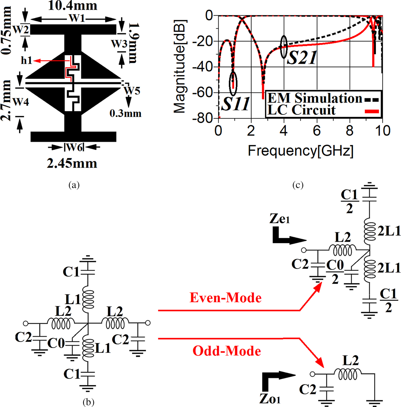
Fig. 1. (a) The geometry of the first resonator with modified T-shaped patches. (b) Its equivalent LC circuit. (c) The EM simulation result of the first resonance cell and the frequency response of its lumped circuit.
To investigate the frequency behavior of the modified T-shaped resonator and identify the importance of each element in controlling the frequency response, the formulas of the transmission coefficient, reflection coefficient, and TZ(s) based on the corresponding even-mode and odd-mode LC circuits [Reference Li, Bao, Du and Wang19, Reference Hong and Lancaster24] shown in Fig. 1(b) are extracted, as expressed by (1–5):
 $$S_{21} = \displaystyle{{Z_{s1}(Z_{e1}-Z_{o1})} \over {(Z_{e1} + Z_{s1})(Z_{o1} + Z_{s1})}},$$
 $$S_{11} = \displaystyle{{Z_{s1}Z_{o1}-Z_{s1}^2} \over {(Z_{e1} + Z_{s1})(Z_{o1} + Z_{s1})}},$$
 $$Z_{e1} = \left[ {\left( {\left. {0.5\left( {2L_1s + \displaystyle{1 \over {0.5C_1s}}} \right)} \right\Vert \displaystyle{1 \over {0.5C_0s}}} \right) + L_2s} \right]\left\Vert {\displaystyle{1 \over {C_2s}}} \right.,$$
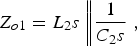 $$Z_{o1} = L_2s\left\Vert {\displaystyle{1 \over {C_2s}}} \right.,$$
 $$f_{z1} = \displaystyle{1 \over {\pi \sqrt {2L_1C_1}}}. $$
Note that, in these equations, Z s1, Z e1, and Z o1 stand for source impedance, even-mode, and odd-mode input impedances, respectively. As can be observed from (1–5), S 21, S 11, and f z1 are depended on (L 1) and (C 1). Therefore, the transmission coefficient, reflection coefficient, and the TZ can be controlled by these valuables and consequently by their corresponding microstrip equivalent. Figures 2(a) and 2(b) depict how changing the mentioned capacitance and inductance can influence the calculated S 21, S 11, and f z1. As can be seen, increase in C 1 from 0.54 to 2.09 pF with the determined steps decreases both the operating frequency and the TZ's frequency.
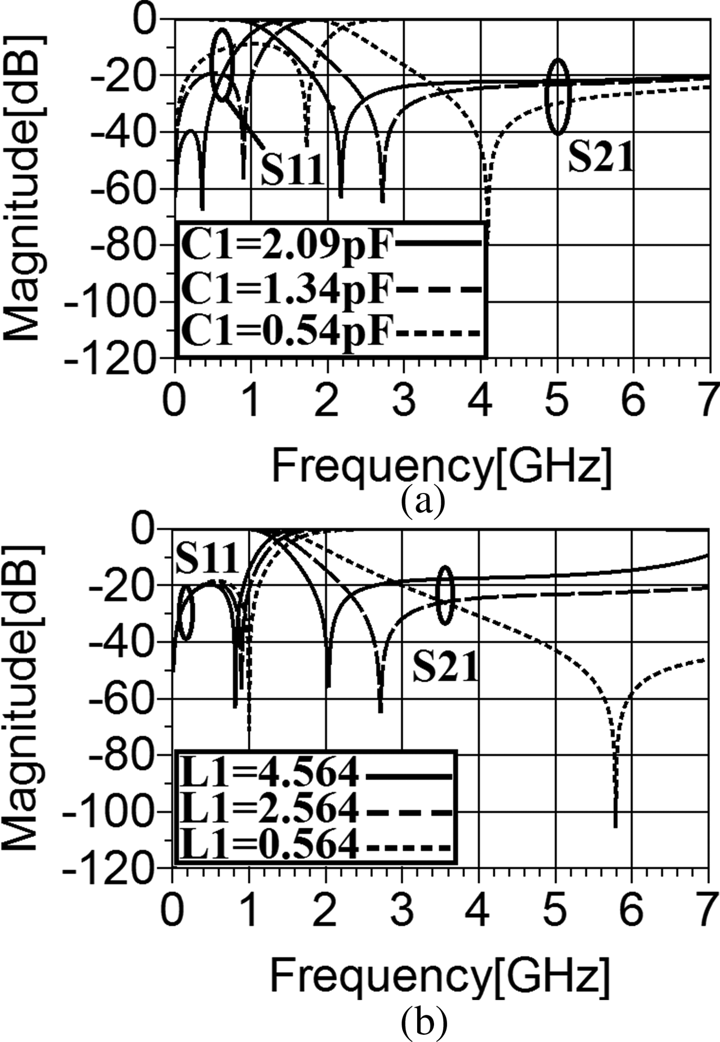
Fig. 2. (a) The calculated S 21 and S 11 as functions of C 1. (b) The calculated S 21 and S 11 as functions of L 1.
Moreover, these increases create a better return loss and to some extend a sharper transition band. On the other hand, as shown in Fig. 2(b), by enhancing the value of the inductance determined by (L 1) from 0.564 to 4.564 nH with steps of 2, the skirt performance becomes considerably steeper as the TZ moves toward the operating frequency. Simultaneously, the −3 dB cut-off frequency goes toward lower frequencies. In this case, the return loss is not influenced noticeably. In the next step, the corresponding microstrip realizations of the most effective lumped elements of the first resonator, i.e. C 1 and L 1, will be studied, as can be observed in Fig. 3. As mentioned previously, the modified T-shaped patch has been modeled by C 1. Thus, the values of (W2), (W3), and (W4) in Fig. 1(a) can be changed. As can be seen in Figs 3(a)–3(c), by increasing the values of these valuables, both the TZ and the −3 dB cut-off frequency move toward lower frequencies. Moreover, enhancing the values of the dimensions determined by (W2), (W3), and (W4) leads to obtaining a better return loss. Similarly, enhancing the length of the high-impedance line of the first microstrip resonator shown in Fig. 1(a) determined by (h1) can sharpen the transition band effectively, without any remarkable impact on the return loss and the −3 dB operating frequency, as depicted in Fig. 3(d).
Fig. 3. The frequency behavior of the first resonator against changing. (a) The value of (W4). (b) The value of (W3). (c) The value of (W2). (d) The value of (h1).
The same procedure to comprehend the frequency behavior of the second main resonator with polygon patches and its LC circuit displayed in Figs 4(a) and 4(b), respectively, can be followed. In Fig. 4(b),  $C_1^{\prime} $ and
  $L_1^{\prime} $ account for the polygon patch and its high-impedance line,
  $C_0^{\prime} $ and
  $C_2^{\prime} $ model the capacitances created between the microstrip structure and the ground.
  $L_2^{\prime} $ and
  $L_3^{\prime} $ represent the inductances of the connecting line. The gap between the coupled polygon patches is modeled by C g. The values of the employed lumped elements in Fig. 4(b) are as follows [Reference Hong and Lancaster24]:
  $C_0^{\prime} $= 0.564 pF,
  $C_1^{\prime} $ = 0.608 pF,
  $C_2^{\prime} $ = 1.3 fF, C g = 2.91 fF,
  $L_1^{\prime} $ = 2.7725 nH,
  $L_2^{\prime} $ = 2.286 nH,
  $L_3^{\prime} $ = 9.86 nH.

Fig. 4. (a) The geometry of the second resonator with its polygon patches. (b) Its LC equivalent circuit. (c) The EM simulation result of the second resonance cell and the frequency response of its lumped circuit.
As displayed in Fig. 4(b), this resonator operating at −3 dB cut-off frequency of 1.8 GHz creates two TZs at 3.542 and 4.271 GHz with attenuation levels of 72.387 and 64.027 dB, respectively. These TZs bring about a stopband covering a frequency band from 2.86 to 6.43 with a suppression level better than 20 dB.
In the following lines, the described LC circuit is utilized to investigate the scattering parameters of the second main resonator.
According to the depicted even-mode and odd-mode LC circuits [Reference Hong and Lancaster24] in Fig. 4(c), the functions of the transmission coefficient, reflection coefficient, and TZ(s) can be given by (6–10):
 $$S_{21}^{\prime} = \displaystyle{{Z_{s2}(Z_{e2}-Z_{o2})} \over {(Z_{e2} + Z_{s2})(Z_{o2} + Z_{s2})}},$$
 $$S_{11}^{\prime} = \displaystyle{{Z_{s2}Z_{o2}-Z_{s2}^2} \over {(Z_{e2} + Z_{s2})(Z_{o2} + Z_{s2})}},$$
 $$\eqalign{Z_{O2} & = \left[ {\left[ {\left( {0.5\left( {\left( {\displaystyle{1 \over {C_1^{\prime} s}}\left\Vert {\displaystyle{1 \over {2C_gs}}} \right.} \right) + L_1^{\prime} s} \right)} \right)\left\Vert {\displaystyle{{L_3^{\prime} s} \over 2}} \right.\left\Vert {\displaystyle{1 \over {C_0^{\prime} s}}} \right.} \right] + L_2^{\prime} s} \right] \cr & \times \left\Vert {\displaystyle{1 \over {C_2^{\prime} s}}} \right.},$$
 $$Z_{e2} = \left[ {\left( {0.5\left( {\displaystyle{1 \over {C_1^{\prime} s}} + L_1^{\prime} s} \right)\left\Vert {\displaystyle{1 \over {C_0^{\prime} s}}} \right.} \right) + L_2^{\prime} s} \right]\left\Vert {\displaystyle{1 \over {C_2^{\prime} s}}} \right.,$$
 $$f_{z1},f_{z2} = \displaystyle{1 \over {2\pi}} \sqrt {\displaystyle{{C_1^{\prime} L_3^{\prime} + C_gL_1^{\prime} \pm \sqrt {2L_1^{\prime} C_1^{\prime} L_3^{\prime} C_g + 2C_gL_1^{^{\prime}2} + C_g}} \over {2C_gC_0^{\prime} + C_1^{^{\prime}2} L_3^{^{\prime}2}}}}. $$
 In these equations,  $C_1^{\prime} $,
  $L_1^{\prime} $, and C g, which represent their microstrip equivalent role, can play noticeable parts in dominating the frequency response. Therefore, three main features of (S 21), i.e. the sharpness of transition band, the wideness and deepness of stopband can be improved by manipulating the dimensions of the microstrip structures modeled by
  $C_1^{\prime} $,
  $L_1^{\prime} $ and the gap shown by C g. This can be proved by studying the behavior of the calculated formulas expressed by (6–10) when the mentioned lumped elements are changed.
As can be understood from Fig. 5(a), the operating frequency, the sharpness, and the suppression level are depended on the value of  $C_1^{\prime} $. For example, the capacity of
  $C_1^{\prime} $ enhances both TZs and also the −3 dB cut-off frequency moves toward lower frequencies. The movement of these TZs leads to a better transition band and a deeper but narrower stopband, as the frequency band between the mentioned zeros decreases. According to Fig. 5(b), in term of improving the skirt performance without influencing the operating frequency considerably, the value of
  $L_1^{\prime} $ can be enhanced; however, this increase affects the stopband features undesirably. The capacitance, which determines the coupling effect of front resonators shown by C g, plays a vital role in creating a TZ and also sharpening the roll-off rate. The frequency behavior of the second main resonator based on the calculated S-parameters expressed by (6–10) against the development of the coupling effect has been illustrated in Fig. 5(c). Obviously, there is just one TZ when C g is equal to zero. The same result could be obtained mathematically by the formula expressed by (10), since setting C g = 0 yields coincident roots or equal TZs. As the coupling capacitance develops, the TZs become more separated without any effect on the −3 dB cut-off frequency. Surprisingly, no considerable influence on the return loss is seen while changing the values of
  $C_1^{\prime} $,
  $L_1^{\prime} $, or C g.
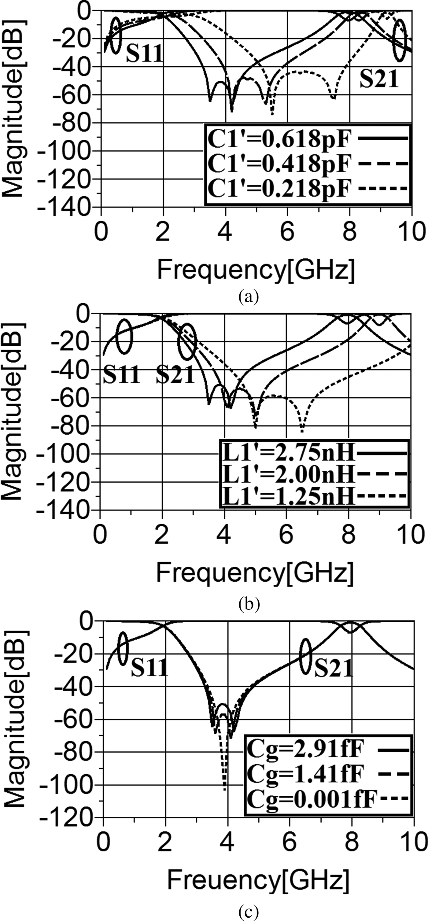
Fig. 5. The calculated S 21 and S 11 as functions of (a)  $C_1^{\prime} $, (b)
  $L_1^{\prime} $, (c) C g.
Now, similar to the first resonator, the microstrip realization of the second resonator will be studied. The polygon patches have been modeled by  $C_1^{\prime} $. Therefore, the dimensions determined by (W7), (W8), and (W9) in Fig. 4(a) can be changed. As illustrated in Figs 6(a)–6(c), by enhancing the values of these valuables, both the TZs and the −3 dB cut-off frequency moves toward lower frequencies. Moreover, decreasing the gap determined by (W10) causes a better return loss and also sharper skirt performance, as shown in Fig. 6(d). Moreover, when the length of the high-impedance line of the second resonator determined by (h2) increases, the steepness of the transition band becomes better, without any noticeable effect on the return loss, as illustrated in Fig. 6(e).
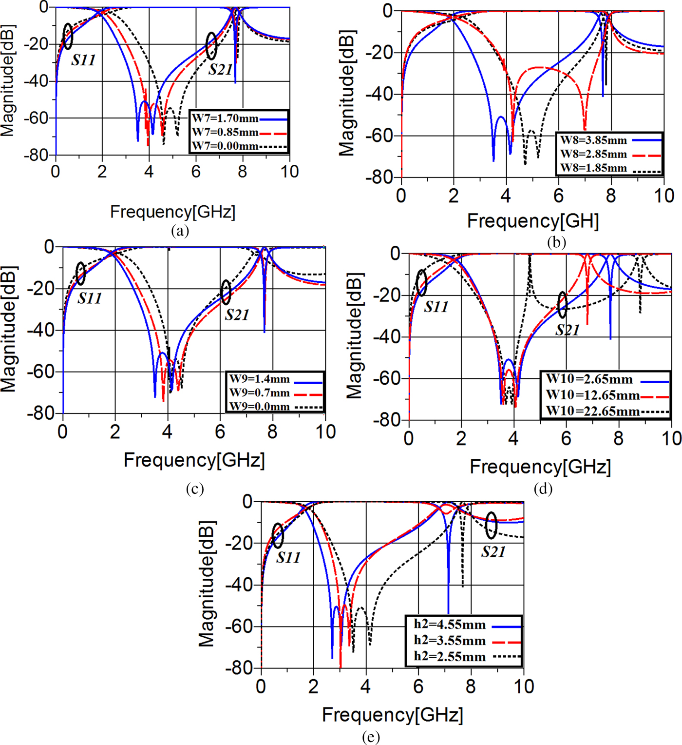
Fig. 6. The frequency behavior of the first resonator against changing. (a) The value of (W7). (b) The value of (W8). (c) The value of (W9). (d) The value of (W10). (e) The value of (h2).
Unfortunately, the introduced resonance cells do not have desired frequency responses, separately. Connecting the proposed resonators shown in Figs 1(a) and 4(a) in series can affect the stopband region due to creating some TZs at different frequencies [Reference Hong and Lancaster24]. Figure 7(a) shows the combination of the first and second resonators.
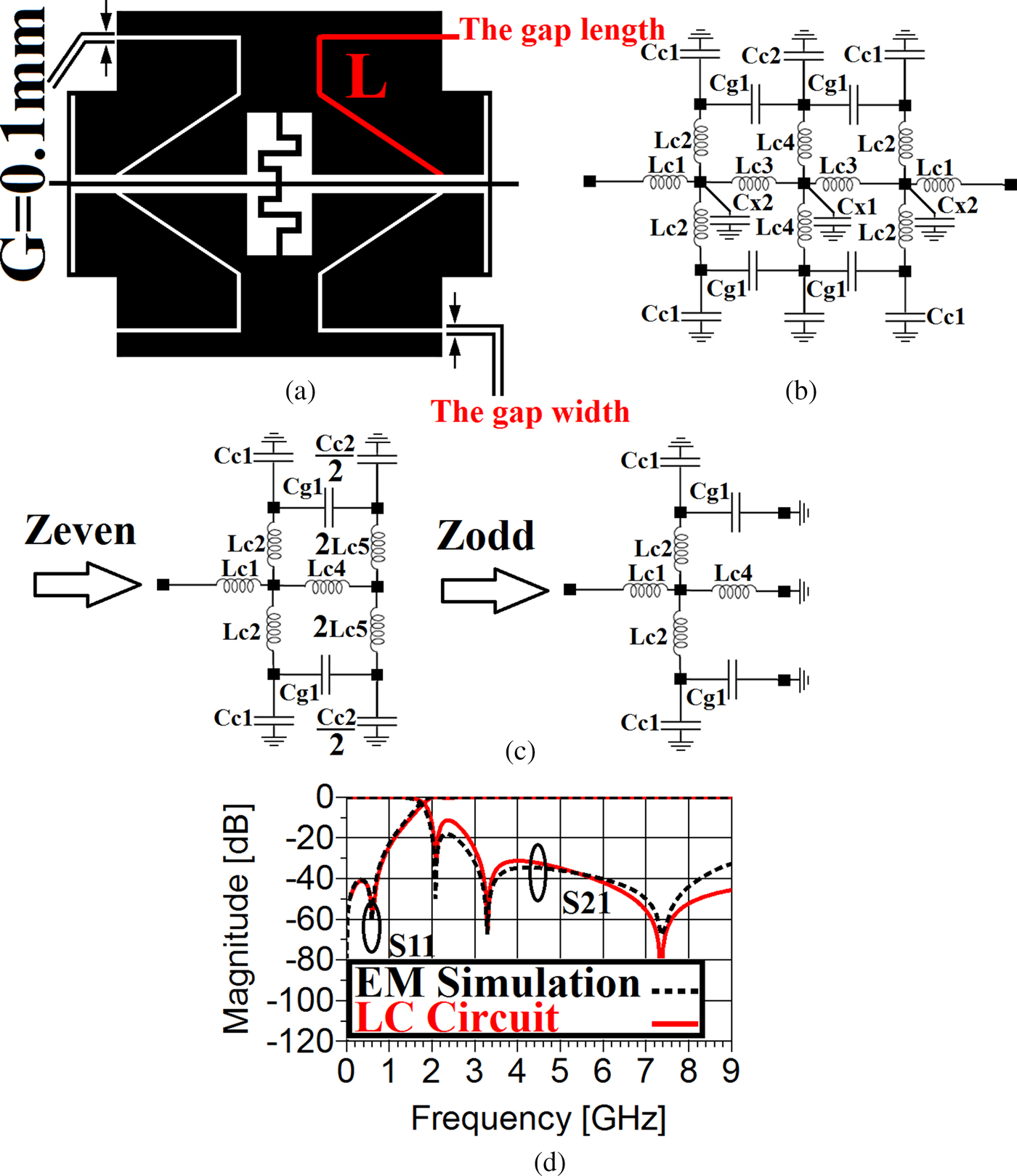
Fig. 7. (a) The combination of the first and second resonators. (b) Its equivalent LC circuit [Reference Hong and Lancaster24] (L c1 = 1.85 nH, L c2 = 1.5 Nh, L c3 = 3.61 nH, L c4 = 6.54 nH, C c1 = 0.635 pF, C c2 = 0.72 pF, C x1 = 0.0635 pF, C x2 = 0.035 pF, C g1 = 0.0954 pF). (c) Even-mode and odd-mode excitations. (d) The EM simulation result of the second resonance cell and the frequency response of its lumped circuit.
This combination, which can be considered as the main resonator, is capable of providing a better skirt performance and stopband characteristics through affecting the locations of the TZs of the first and second resonators. To determine how the coupling effect between the employed resonators can affect the frequency response and also how the connected cells in series complete the performance of each other through their TZs, the formulas of S 21 and S 11 of the equivalent LC circuit of the main resonator shown in Fig. 7(b) are extracted. In the LC circuit, the coupling effect between the first and second resonators is modeled by C g1. According to the illustrated even-mode and odd-mode lumped circuits in Fig. 7(c), the transmission coefficient and reflection coefficient can be expressed by (11–20):
 $$S_{21}^{^{\prime\prime}} = \displaystyle{{Z_{sc}(Z_{ec}-Z_{oc})} \over {(Z_{ec} + Z_{sc})(Z_{oc} + Z_{sc})}},$$
 $$S_{11}^{^{\prime\prime}} = \displaystyle{{Z_{sc}Z_{oc}-Z_{sc}^2} \over {(Z_{ec} + Z_{sc})(Z_{oc} + Z_{sc})}},$$
 $$Z_{oc} = \displaystyle{{s[L_{c4} + s^2L_{c2}L_{c4}(C_{g1} + C_{c1})]} \over {1 + s^2L_{c2}L_{c4}(C_{g1} + C_{c1})}},$$
 $$Z_{ec} = M + N,$$
 $$M = \displaystyle{{Z_1Z_2 + Z_1Z_3 + Z_2Z_3 + {(2s^2C_{c1}C_{c2})}^{-1}} \over {Z_1 + Z_2 + {(2sC_{c1})}^{-1} + {(sC_{c2})}^{-1}}},$$
 $$N = \displaystyle{{(Z_2 + Z_3){(2sC_{c1})}^{-1}-()Z_1 + Z_3{(sC_{c2})}^{-1}} \over {Z_1 + Z_2 + {(2sC_{c1})}^{-1} + {(sC_{c2})}^{-1}}},$$
 $$Z_1 = \displaystyle{{L_{c2}} \over {4(Z_{de}C_{g1})}},$$
 $$Z_2 = \displaystyle{{L_{c5} + L_{c4}} \over {2(Z_{de}C_{g1})}},$$
 $$Z_3 = \displaystyle{{s^2L_{c2}(L_{c4} + L_{c5})} \over {Z_{de}}},$$
 $$Z_{de} = s(0.5L_{c2} + L_{c4} + L_{c5}) + (2sC_{g1})^{-1}.$$
Note that, in (11) and (12) Z sc, Z ec, and Z oc are source impedance, even-mode and odd-mode input impedances, respectively. As can be understood from (11–19), the formulas of the scattering parameters are functions of C g1. This means that the coupling effect can be used to control the frequency behavior of the combination of the first and second resonators.
To depict how the transmission coefficient and reflection coefficient are depended on the coupling capacitance determined by C g1, the behavior of the calculated formulas expressed by (11–19) against changing the value of this element from 0 to 95.4 fF with steps of 47.7 has been illustrated in Fig. 8. As can be seen from Fig. 8, when the coupling effect increases, the first TZ becomes closer to the −3 dB operating frequency, which means a sharper transition band. However, the suppression level around the first TZ is affected negatively. Moreover, the cut-off frequency tends to move toward lower frequencies while C g1 enhances. Varying this variable has not influenced S 11 dramatically.
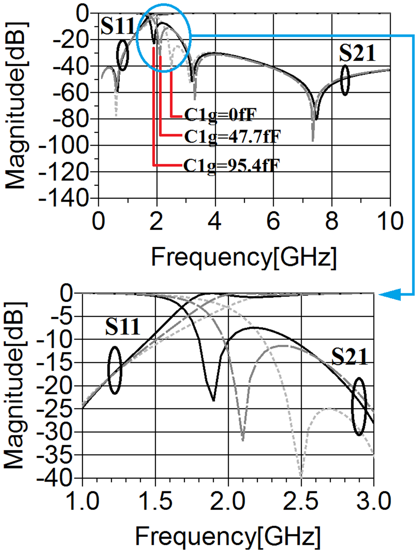
Fig. 8. The behavior of the calculated S 21 and S11 of the combined resonator against changing the value of C g1.
According to Fig. 9, similar results can be obtained when the determined gap by (G) in the microstrip structure illustrated in Fig. 7(a) varies. Clearly, decreasing the value of (G) makes the transition band sharper and the stopband wider. However, as it was expected, the return loss gets affected undesirably.
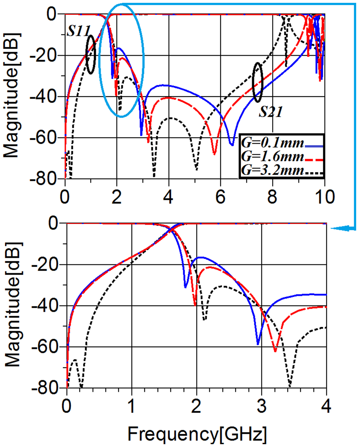
Fig. 9. The behavior of the combined resonator depicted in Fig. 7(a) against changing the gap between the first and second resonators.
Clearly, the increase of the coupling effect in the microstrip realization means decreasing the gap determined by (G) in Fig. 7(a). Note that, the fabrication limitation related to the possible minimum gap restricts the use of this method. On the other hand, to increase the coupling effect, the length of the shown gap in Fig. 7(a), i.e. (L), can be increased instead of decreasing the determined gap width by (G). Therefore, to exploit this technique and increase the shown (L) as much as possible and also control the −3 dB frequency, polygon patches have been employed instead of using the traditional structure introduced in [Reference Hong and Lancaster24]. According to the carried out simulation depicted in Fig. 7(d), the combined resonator operates at 1.63 GHz. In the whole passband area, an insertion loss better than 0.088 dB from DC to 1.076 GHz has been obtained. As can be seen from Fig. 7(d), there are three TZs at 2.17, 3.036, and 7.298 GHz with the corresponding attenuation levels of 50.02, 68.18, and 63.27 dB, respectively, which the first one makes a sharp transition band. The second and third TZs improve the rejection level due to their corresponding suppression levels. The rejection band attenuates spurious frequencies from 3. 14 up to 9 GHz with the corresponding rejection level of 28.35 dB.
The procedure of obtaining the microstrip structure
In this section, the procedure of reaching the primarily T-shaped resonator is explained, step by step. First, a simple lowpass resonator similar to the one introduced in [Reference Hong and Lancaster24], which operates at 1.65 GHz, has been designed as shown in Fig. 10(a). The procedure of designing the primary resonator is explained in the following lines.
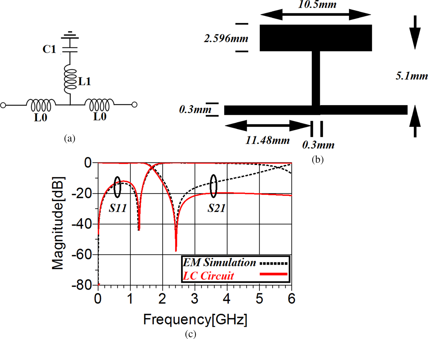
Fig. 10. The conventional method of designing a lowpass resonator operating at −3 dB cut-off frequency of 1.65 GHz. (a) The primary LC circuit. (b) Its equivalent microstrip realization. (c) Their frequency response.
The stepped impedance open stubs introduced in [Reference Hong and Lancaster24] are practical resonance cells due to their ability in producing instant attenuation in the stopband region through making TZs. Cascading these units bring about a wide rejection band, although the occupied area of the obtained filter via the mentioned technique in [Reference Hong and Lancaster24] becomes very large (in particular, when TZs at lower frequencies are required). Therefore, the dimensions of the employed microstrip lines of the resonator need to be optimized. By using the cited procedure in [Reference Hong and Lancaster24], a primary lumped circuit operating at 1.65 GHz is presented. The lumped structure and its frequency response are shown in Figs 10(a) and 10(c), respectively. The values of the employed lumped elements are L 0 = 6 nH, L 1 = 2.66 nH, C 1 = 1.8 pF. Now, the given lumped resonator has to be converted to its corresponding microstrip realization, which is carried out by converting each lumped element to its microstrip equivalent utilizing (20) and (21):
 $$l = CZ_c\nu _p,$$
 $$l = \displaystyle{{L\nu _p} \over {Z_c}},$$
where (l) is the length of the microstrip line when its width is regarded constant. Moreover, C and L are the capacitance and inductance of the depicted LC circuit in Fig. 10(a), respectively; Z c and υ p are the characteristic impedance and the phase velocity, respectively. The above-mentioned variables can be obtained as follows:
 $$\nu _p = \displaystyle{c \over {\sqrt {\varepsilon _{re}}}}. $$
For w/h ≤ 1:
 $$\varepsilon _{re} = \displaystyle{{\varepsilon _{r + 1}} \over 2} + \displaystyle{{\varepsilon _{r-1}} \over 2}\left\{ {{\left[ {1 + 12\displaystyle{h \over w}} \right]}^{-0.5} + 0.04{\left[ {1-\displaystyle{w \over h}} \right]}^2} \right\},$$
 $$Z_c = \displaystyle{\eta \over {2\pi \sqrt {\varepsilon _{re}}}} \ln \left[ {8\displaystyle{h \over w} + 0.25\displaystyle{w \over h}} \right].$$
For w/h ≥ 1:
 $$\varepsilon _{re} = \displaystyle{{\varepsilon _{r + 1}} \over 2} + \displaystyle{{\varepsilon _{r-1}} \over 2}\left[ {1 + 12\displaystyle{h \over w}} \right]^{-0.5},$$
 $$Z_c = \displaystyle{\eta \over {\sqrt {\varepsilon _{re}}}} \left\{ {\displaystyle{w \over h} + 1.393 + 0.677\ln \left[ {\displaystyle{w \over h} + 1.444} \right]} \right\}^{-1},$$
where w, h, and (ε r) are the width of the microstrip line, the thickness, and permittivity of the substrate, respectively. Moreover, (ε re) represents the effective permittivity, and the parameter (η) is a constant equal to 120 πΩ and (c) represents the light speed. For a chosen microstrip transmission line with w = 0.3 mm, the values of (ε re) and (Z c) are equal to 2.5 and 99.13 Ω, respectively. Similarly, when w = 10.5 mm, the related equations, i.e. (25) and (26), yield ε re = 3.244 and Z c = 8.66 Ω. Regarding the expressed formulas by (20) and (21), the microstrip realization of the shown LC circuit in Fig. 10(a) can be attained, as depicted in Fig. 10(b). Note that the utilized substrate is a 0.508 mm-thick substrate with a relative dielectric constant of 3.5, and a loss tangent of 0.0018.
The dimensions and the frequency response of this resonator have been shown in Figs 10(b) and 10(c), respectively. Obviously, there is a reasonable correlation between the frequency responses of the equivalent LC circuit and its microstrip structure. As can be seen, the microstrip realization does not have an acceptable frequency response, which proves that there is a need for optimization. The process of achieving an optimized T-shaped resonator has been shown in Fig. 11, step by step. Figure 11(a) shows how the primary resonator depicted in Fig. 10(b) has been changed, to obtain a better stopband characteristic. As shown in Figs 11(b) and 11(c), adding the transmission line determined by a blue microstrip line and employing the meandered transmission line not only have widened the stopband with a better rejection level, but also have improved the return loss significantly. To achieve a better stopband feature, two of the shown cells in Fig. 11(b) have been placed symmetrically around (X)-axis. However, the transition band has been affected negatively. To obtain an acceptable frequency response with a better rejection band, several stages of the mentioned T-shaped structure are needed [Reference Hong and Lancaster24]. Thus, similar to the method employed in the design of the resonator shown in Fig. 11(a), four more T-shaped resonators have been designed and applied to the depicted cell in Fig. 12(a).
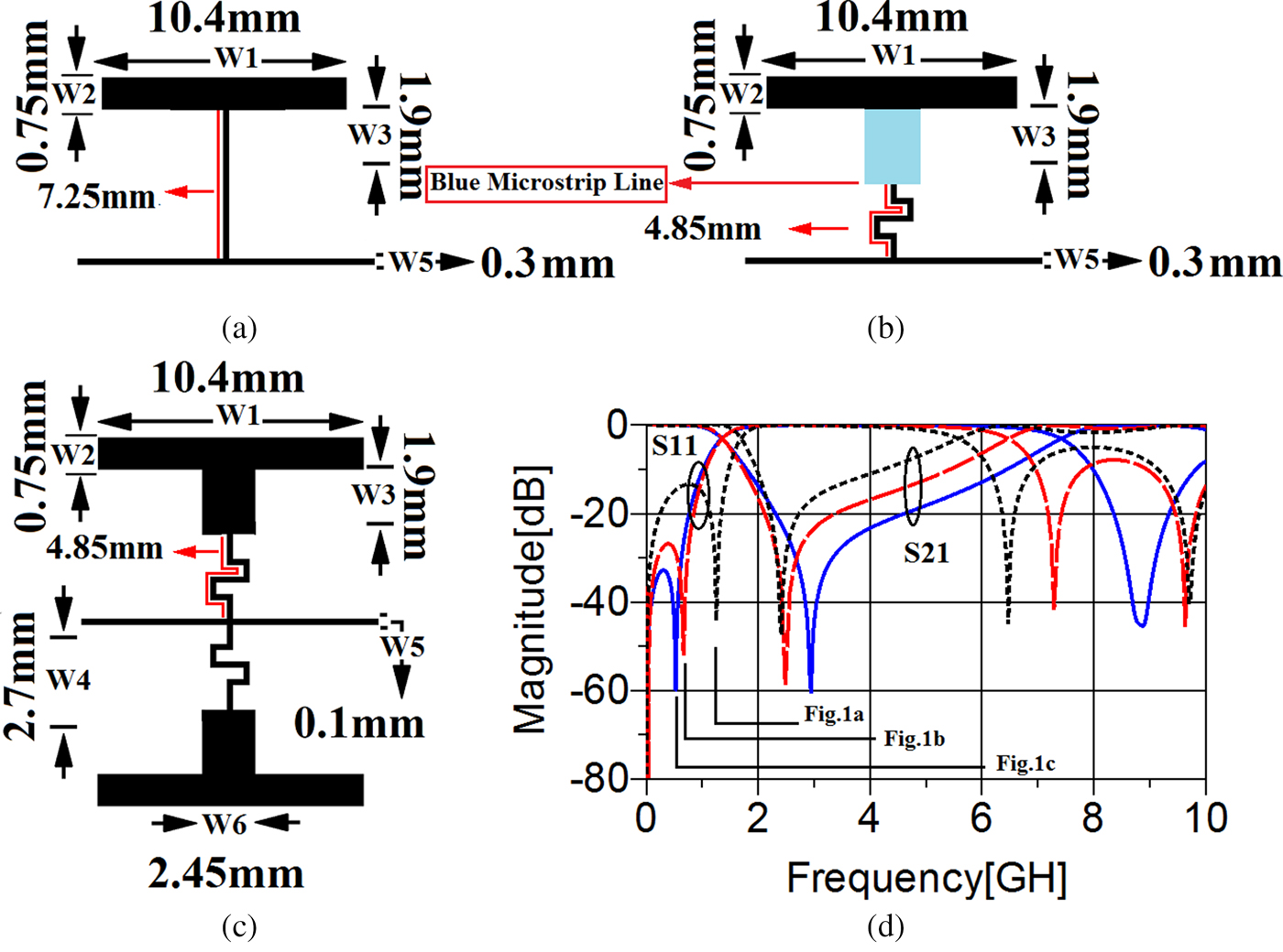
Fig. 11. The steps of designing the optimized T-shaped resonator. (a) The primary structure. (b) Adding the blue microstrip transmission line. (c) Obtaining a symmetrical structure using the shown resonator in (b). (d) The frequency response of the shown resonators in (a–c), separately.
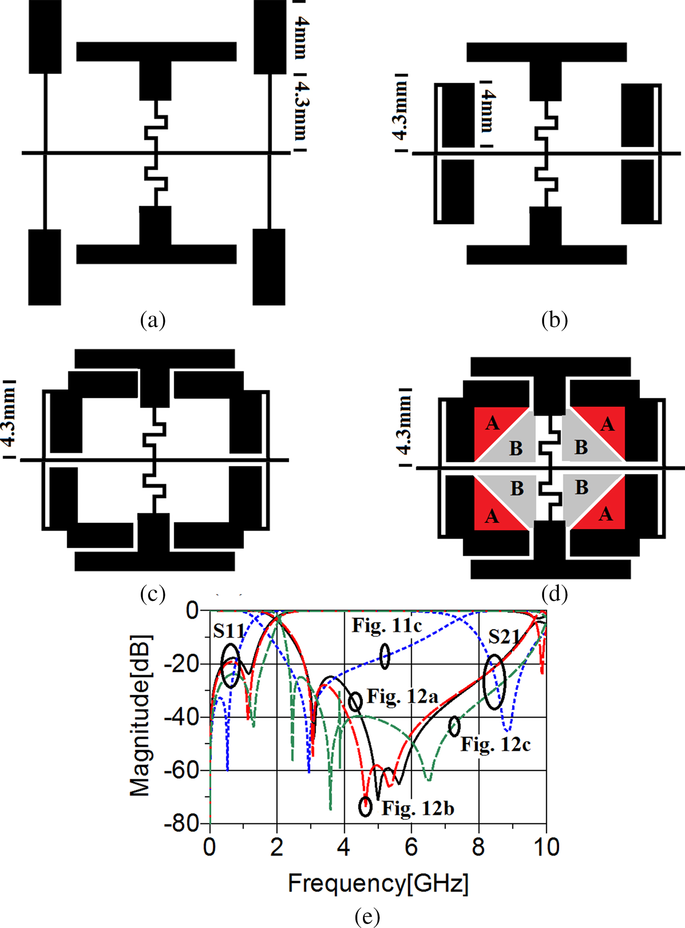
Fig. 12. The procedure of obtaining the combined structure. (a) Employing four new T-shaped resonators. (b) Folding them to decrease the circuit size. (c) Adding rectangular patches to increase the coupling effect between the first and second resonators. (d) Employing triangular patches to enhance the coupling effect between the first and second resonators and control the −3 dB cut-off frequency. (e) The frequency response of the shown circuits in Figs. 11(c) and 12(a)–12(c), separately.
Note that, these new T-shaped cells have to create some TZs at upper frequencies to broaden the stopband bandwidth. Figure 12(a) shows how these new resonators have been applied to the structure shown in Fig. 11(c). As can be seen from the frequency response, employing the new T-shaped cells has created two more TZs at 5 and 5.62 GHz leading to expanding the stopband from 2.79 to 8.61 GHz as shown in Fig. 12(e). But the return loss and, to some extent, the transition band have been influenced negatively. Before solving these problems, to decrease the occupied area, the new T-shaped cells have been folded, as shown in Fig. 12(b). Fortunately, this not only leads to a decrease in the circuit size, but also has brought about a better suppression level from 2.79 to 8.61 GHz.
As discussed in [Reference Li, Bao, Du and Wang19] and proved in Figs 8 and 9, increasing the coupling effect between the two main resonators not only widen the stopband bandwidth, but also sharpen the transition band. One way to increase the coupling effect between the two main resonators has been shown in Fig. 12(c). Comparing the frequency response of the circuit after and before adding the rectangular parts proves that both the skirt performance (from 2.1 to 2.455 GHz with corresponding attenuation levels of −3 and −60 dB, respectively) and the rejection band (from 2.35 to 9.4 GHz with a suppression level of −21 dB) have been improved significantly. Moreover, in comparison to the frequency response of the resonator shown in Fig. 12(b), a better return loss has been achieved, as shown in Fig. 12(e). However, the operating frequency and the steepness of the transition band are not desired yet. To have a desired −3 dB operating frequency, the first resonator can play a vital role. Clearly, increasing the occupied area of the T-shaped patches can be the easiest technique. Thus, the remained free space between the first and second resonators determined by (A) and (B) can be used. Adding the shown triangular patches in Fig. 12(d) leads to sharpening the skirt performance as the coupling effect between the proposed resonators increases and shifting the −3 dB cut-off frequencies to a desired value as the occupied area of the T-shaped patch enhances, respectively.
The final resonator composing of the first resonator with the modified T-shaped patches and the second one with the polygon patches and its frequency response has been shown in Figs 12(d) and 12(e), respectively.
Unfortunately, the rejection band of the combined resonator is not wide enough. Therefore, producing some more TZs at higher frequencies can omit spurious frequencies over a wide range and broaden the stopband. To improve the rejection band performances, 10 coupled suppressors, i.e. eight high–low impedance folded stubs and two rectangular open-stubs, are located on both sides of the combined resonators illustrated in Fig. 12(d). The procedure of applying these attenuators to the shown resonator in Fig. 12(d) is described step by step. The configuration of the first suppressors, its dimensions, how it has been applied to the main resonator, and how it has affected the frequency response are shown in Fig. 13.
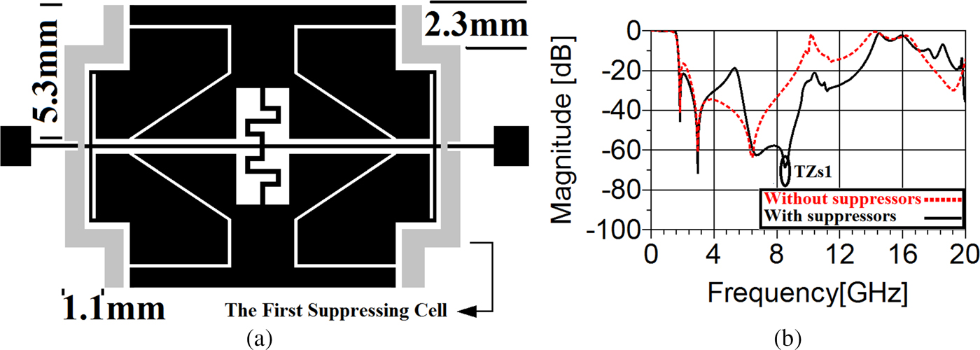
Fig. 13. (a) The configuration of the main resonator with its first suppressing cell. (b) The frequency response of the circuit with its first suppressor in comparison to the main resonator without suppressors.
Clearly, employing this attenuator creates a TZ (TZs1) located on 8.507 GHz with a corresponding attenuation level of 69.045 dB leading to suppressing spurious frequencies from 9.163 to 13.15 GHz, where the main resonator was not able to omit them. Cascading another attenuator can produce new TZs at higher frequencies resulting in a better stopband performance.
Figure 14(a) shows the schematic representation of the main resonator with its both suppressors. Figure 14(b) illustrates the effects of adding the second suppressing cell on the frequency response of the shown structure in Fig. 13(a). As can be observed from the result of the simulation shown in Fig. 14(b), applying the second suppressing cell makes two more TZs with attenuation levels better than 40 dB, i.e. TS2 and TS3 at frequencies higher than the frequency of TS1.
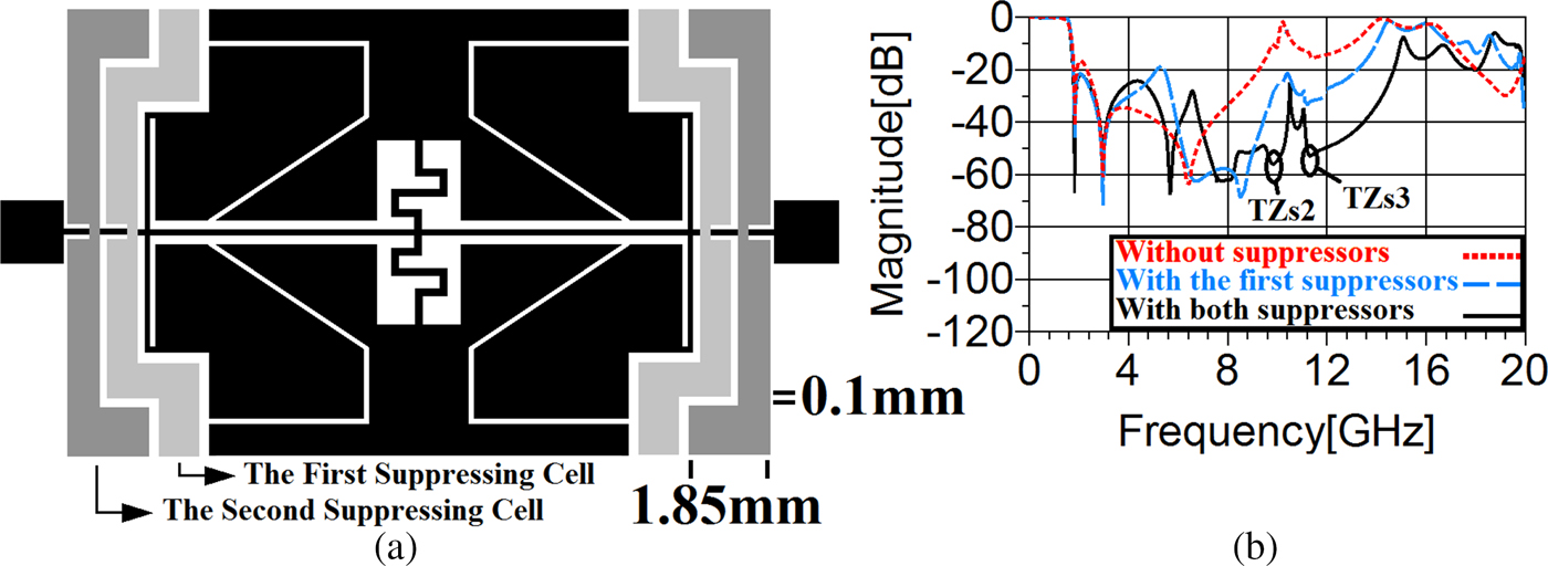
Fig. 14. (a) The schematic representation of the main resonator with two suppressors. (b) Its frequency response in comparison to the main resonator with and without the first suppressor.
These TZs lead to attenuating spurious signals from 11.85 to 14.72 with a better suppression level in comparison to the frequency response of the main resonator with and without the first suppressor (see Fig. 14(b)).
To improve the rejection band performance up to at least 10fc, another suppressor is needed, but the occupied area of the final LPF is an important issue. To expand the stopband region without increasing the circuit size considerably, four rectangular open-stubs are utilized (see Fig. 15(a)).
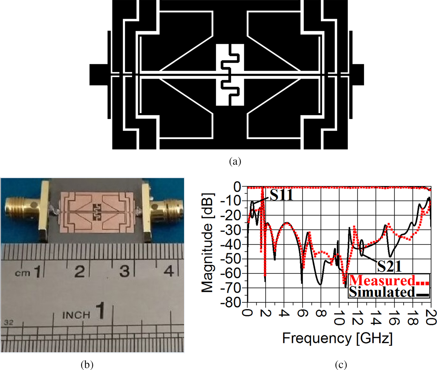
Fig. 15. The proposed LPF. (a) The schematic representation of the proposed LPF. (b) The photograph of the proposed LPF. (c) The results of simulation and measurement.
Finally, an LPF with wide stopband and steep transition band operating at 1.65 has been achieved (see Fig. 15(c)).
The results of simulation and measurement
The geometry and photograph of the presented filter are depicted in Figs 15(a) and 15(b), respectively. This filter is fabricated on RO4003 substrate (dielectric constant = 3.38, thickness = 0.508 mm). To perform the shown simulations and measurements in Fig. 15(c), which are in good consistency, Agilent's ADS Electromagnetic simulator software and HP 8720B vector network analyzer have been used. As illustrated in Fig. 15(c), the proposed filter has a −3 dB cut-off frequency of 1.65 GHz. According to the measurement results, the return loss and the insertion loss are better than 15.85 and 0.0763 in the passband region. The proposed filter makes a TZ located at 1.831 GHz with the corresponding suppression level of 62.33 dB close to the operating frequency. Therefore, a steep transition band from 165 to 1.744 GHz with the corresponding attenuation levels of −3 and −40 dB, respectively, is achieved. This skirt performance corresponds to a roll-off rate equal to 393.61 (dB/GHz). The stopband region stops spurious frequencies ranging from 1.695 to 18.34 GHz with an attenuation level of 23 dB. The circuit size of this LPF is 18.15 mm × 10.9 mm.
Performance comparison of the designed LPF with the cited references has been shown in Table 1. In the provided table, the roll-off rate (ξ) can be obtained as follows:
 $$\xi = \displaystyle{{\alpha _{\max} -\alpha _{\min}} \over {\,f_S-f_C}}\quad ({\rm dB}/{\rm GHz}).$$
Table 1. The performance comparison of the designed LPF with the mentioned references

In this formula, α max represents the 40 dB attenuation point, α min represents the 3 dB attenuation point, f S is the 40 dB stopband frequency, and f C is the −3 dB cut-off frequency.
The relative stopband bandwidth (RSB) can be expressed as follows:
 $${\rm RSB} = \displaystyle{{{\rm stopband}\quad {\rm band}\,{\rm width}\,(-20\,{\rm dB})} \over {{\rm stopband}\quad {\rm center}\,{\rm frequency}}}.$$
The suppression factor (SF) is defined as depicted in equation (29). For example, when the stopband suppression is 23, the corresponding SF will be 2.3:
 $${\rm SF} = \displaystyle{{{\rm stopband}\quad {\rm supression}} \over {10\,{\rm dB}}}.$$
The normalized circuit size (NCS) can be obtained by:
 $${\rm NCS} = \displaystyle{{{\rm physical}\;{\rm size}\,({\rm length} \times {\rm width})} \over {\lambda _g^2}}, $$
where (λ g) is the guided wavelength at −3 dB cut-off frequency.
The architecture factor (AF) expresses the circuit complexity. When we have a two-dimensional circuit, AF will be equal to one. Likewise, for three-dimensional structures, we have AF = 2.
Finally, the figure-of-merit (FOM) can be calculated as follows:
 $${\rm FOM} = \displaystyle{{\xi \times {\rm RSB} \times {\rm SF}} \over {{\rm NCS} \times {\rm AF}}}.$$
According to the above-mentioned formulas expressed by (27–31), calculating the values of roll-off rate (ξ), RSB, SF, NCS, and AF of the presented filter leads to an FOM equal to (81 672).
Conclusion
An LPF adopting meandered lines loaded by modified T-shaped and polygon patches and also 10 cells with different structures playing the role of suppressors has been proposed and fabricated. By using even-mode and odd-mode analysis, the functions of the transmission coefficient, reflection coefficient, and consequently TZs of the main resonators based on their lumped circuits have been calculated. The scattering parameters of the implemented LPF confirm good in-band and out-band characteristics. According to the measurement results, the presented filter provides a steep transition band, a wide stopband, and acceptable return loss and insertion loss in the passband. The fabricated filter has brought about a FOM equal to 81 672.
 Mohsen Hayati received the B.E. degree in Electronics and Communication Engineering from Nagarjuna University, Andhra Pradesh, India, in 1985, and the M.E. and Ph.D. degrees in Electronics Engineering from Delhi University, Delhi, India, in 1987 and 1992, respectively. He joined the Electrical Engineering Department, Razi University, Kermanshah, Iran, as an Assistant Professor in 1993. Currently, he is a Professor with the Electrical Engineering Department, Razi University, Kermanshah, Iran. He has published more than 230 papers in international, domestic journals, and conferences. His current research interests include microwave and millimeter-wave devices and circuits, application of computational intelligence, artificial neural networks, fuzzy systems, neuro-fuzzy systems, electronic circuit synthesis, modeling, and simulations.
 Ashkan Abdipour received the B.S degree in Electronics Engineering, from Islamic Azad University, Kermanshah Branch, Kermanshah, Iran, in 2009 and the M.S degree from Razi University, Kermanshah, Iran, in 2013. His research interest includes microwave and millimeter-wave devices and circuits.
 Arash Abdipour received the B.S degree in Electronics Engineering, from Islamic Azad University, Kermanshah Branch, Kermanshah, Iran, in 2009 and the Master's degree in Electronics Engineering from the Kermanshah-science and research University of Kermanshah Branch, Kermanshah, Iran, in 2013. His research interest includes microwave and millimeter-wave devices and circuits.


