I. INTRODUCTION
Tunable and reconfigurable filters play an important role in the development of next-generation multi-band communication systems, because they can reduce their overall size dramatically. These components have to be compact and energy-efficient. RF-MEMS reconfigurable filters have demonstrated superior performance (in comparison with components that use active devices), in terms of linearity and power consumption [Reference Rebeiz1, Reference Lucyszyn2]. Most of RF-MEMS planar filters available in the literature use microstrip or coplanar waveguide (CPW) technology.
The CPW offers excellent reconfiguration capabilities because series or shunt components (such as RF-MEMS switches or varactors) can be easily mounted on it. Many uniplanar circuits replicate classical (monomodal) filter structures, even though the CPW is a multimodal transmission line that can simultaneously propagate two fundamental modes, i.e. even and odd. The even mode is commonly used in CPW circuits. The odd mode, which is compatible with the slotline mode, is often considered as spurious and suppressed, wherever it may be generated (as for instance in CPW asymmetric shunt impedances [Reference Ribó and Pradell3]), by means of air-bridges. However, it offers a further degree of freedom that can be used to achieve new filter topologies, as demonstrated in [Reference Contreras, Pradell and Ribó4, Reference Contreras, Ribó, Pradell and Blondy5].
In this paper, a new quarter-wavelength multimodal second-order bandpass filter with two reconfigurable center frequencies (f 01 = 12 GHz and f 02 = 13 GHz) and constant 3-dB fractional bandwidth (FBW) between the two frequency states is presented. The filter uses two multimodal CPW-to-slotline transitions, which act as input/output multimodal immitance inverters (MIIs) [Reference Contreras, Ribó, Pradell and Blondy5]. It was fabricated using the RF-MEMS integrated technology of Fondazione Bruno Kessler (FBK) [Reference Giacomozzi, Mulloni, Colpo, Iannacci, Margesin and Faes6]. The filter reconfiguration capability is achieved using RF-MEMS switchable air-bridges (SABs) [Reference Contreras7] in both MIIs.
II. FILTER DESIGN
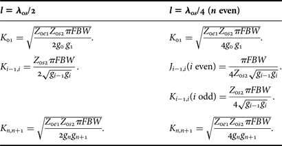
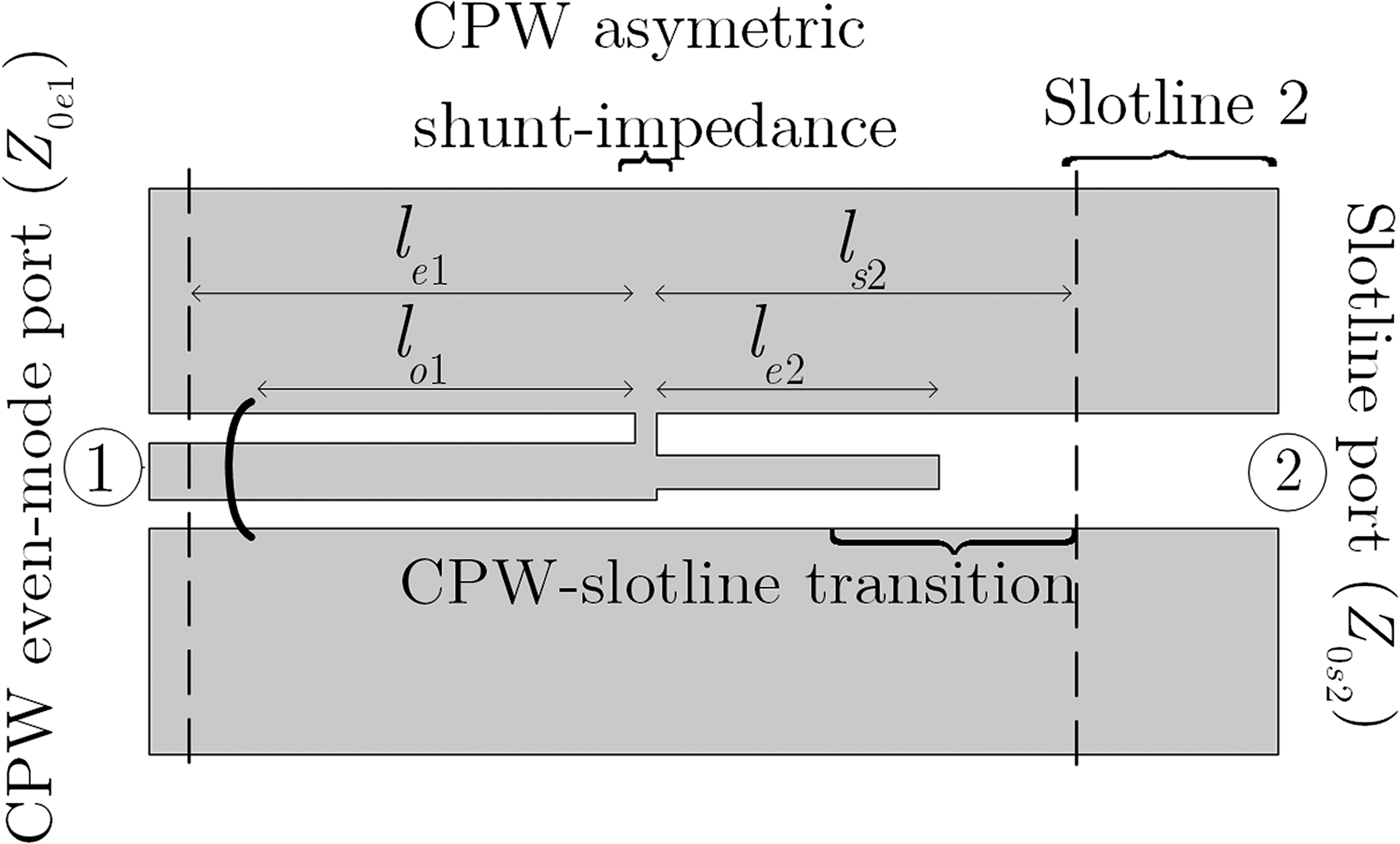
The proposed filter is based on the coupled-resonator structure shown in Fig. 1, whose normalized inverter values are summarized in Table 1. Coupled-resonator filters can use half-wavelength (l = λ 0s/2) or quarter-wavelength (l = λ 0s/4) resonators [Reference Contreras, Ribó, Pradell and Blondy5], where λ 0s denotes the wavelength for the resonator transmission lines at the filter center frequency.

Fig. 1. Generic coupled-resonator filter structure. Z 0e1 and Z 0s2 are the reference impedance for the filter ports and the characteristic impedance of the resonator transmission lines, respectively.
Table 1. Design values for the coupled-resonator filter in Fig. 1.
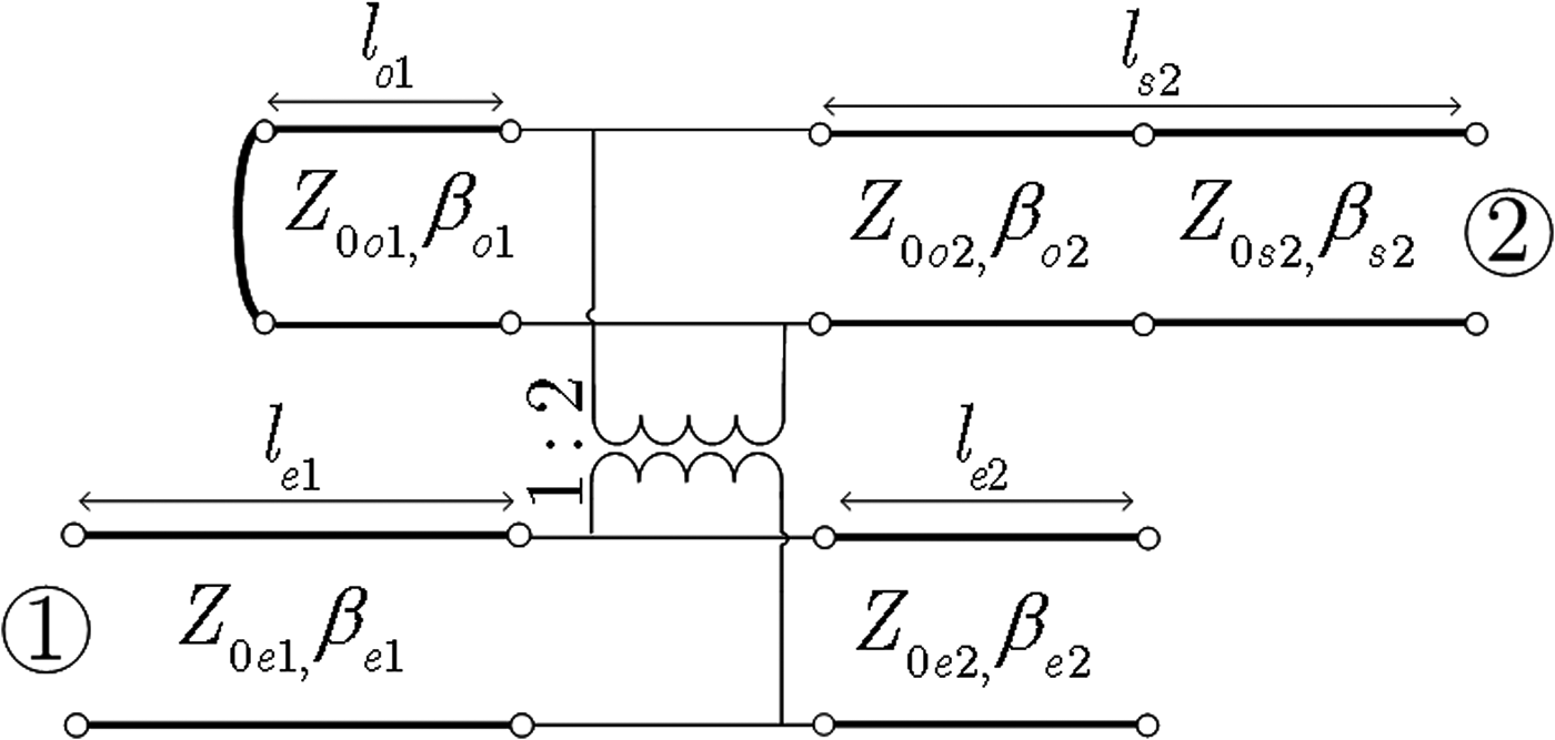
Figure 2 shows a new type of immitance inverter, which was proposed in [Reference Contreras, Ribó, Pradell and Blondy5]. The core of the circuit in Fig. 2 is the asymmetric shunt-short-circuit CPW transition, formed by an asymmetric shunt-short-circuit in one of the CPW slots. The immitance inverter in Fig. 2 can be modeled using the equivalent multimodal circuit depicted in Fig. 3.
Fig. 2. Multimodal immitance inverter (MII).
Fig. 3. Circuit model of the multimodal immitance inverter in Fig. 2. Z 0ei, β ei, Z 0oi, β oi, Z 0s2, and β s2 are, respectively, the characteristic impedances and phase constants of the even and odd modes of CPW i (i=1,2), and of the slotline mode.
Figure 4 shows the layout of a quarter-wavelength slotline-resonator second-order bandpass filter that uses reconfigurable MIIs as first and last inverters [Reference Contreras, Ribó, Pradell and Blondy5] (λ 0s is the wavelength of the slotline mode at the center frequency).
Fig. 4. Filter with quarter-wavelength slotline resonators using MIIs.
Its circuit model is shown in Fig. 5. The MIIs perform an immitance inversion between the CPW even mode of the filter ports and the slotline mode of the resonators by means of a multimodal CPW section (where the CPW even and odd modes propagate simultaneously). This CPW section has a length l o1. The length l s2 can always be chosen negative (if so, l s2 ≈ −l o1 [Reference Contreras, Ribó, Pradell and Blondy5]) and therefore the physical resonator lengths are l r ≈ λ 0s/4. Subscripts e, o, and s refer to the even, odd, and slotline modes, respectively.
Fig. 5. Multimodal circuit model for the filter with quarter-wavelength slotline resonators presented in Fig. 4.
The MIIs can be reconfigured by changing the position of their odd-mode short-circuit (the air-bridge) by means of SABs, as shown in Figs 6 and 7. As a result, the odd-mode length l o1 will be shortened and, since l o1 is part of the physical resonator of length l r (see Fig. 7), l r will also be shortened, producing a frequency shift (increase) in the filter center frequency.
Fig. 6. Frequency-reconfigurable second-order quarter-wavelength filter using MIIs and SABs.
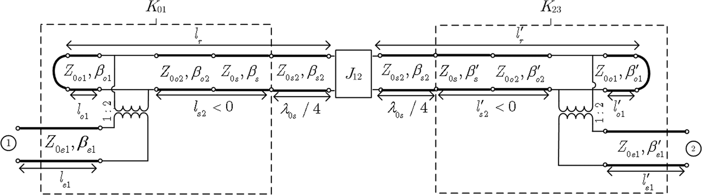
Fig. 7. Circuit model of a frequency-reconfigurable second-order quarter-wavelength filter using MIIs and SABs.
Using the circuit model in Fig. 7 and the theory presented in [Reference Contreras, Ribó, Pradell and Blondy5], the reconfigurable filter can be designed for a given response at the lower frequency (state 1), and the optimal position of the SAB can be parametrically investigated to give an appropriate second (higher) frequency state (state 2). This optimal position is selected to maintain the 3-dB FBW as constant as possible by keeping the change in the ratio l o1/l r as small as possible (since the FBW is a function of l o1/l r [Reference Contreras, Ribó, Pradell and Blondy5]). The effect of the intrinsic inductance and contact resistance of the SAB should be estimated by measurement or by electromagnetic simulation, and then should be taken into account in the circuit simulation.
In contrast to [Reference Contreras, Ribó, Pradell and Blondy5], where the reconfiguration capability was achieved by loading each resonator with a variable capacitance (varactor diode), but leaving the resonator physical length unchanged, in this paper it is achieved by changing the resonator physical length using an RF-MEMS SAB connected at one end of each resonator (see Fig. 6). This new configuration allows a more versatile filter design than in [Reference Contreras, Ribó, Pradell and Blondy5] since the two states of the filter can not only exhibit similar FBW, but also similar insertion loss (IL).
Using this approach, a quarter-wavelength slotline-resonator second-order bandpass filter with reconfigurable center frequency was designed to be implemented using the RF-MEMS integrated technology described in [Reference Giacomozzi, Mulloni, Colpo, Iannacci, Margesin and Faes6]. The chosen even- and odd-mode characteristic impedances are Z 0e = 50 Ω and Z 0o = Z 0s = 78 Ω, respectively. The additional characteristic parameters of the transmission lines, such as the phase constants (β e, β o, and β s) and losses were obtained as described in [Reference Contreras, Ribó, Pradell and Blondy5]. The simulated response of the circuit model for both states is shown in Fig. 8. As can be seen, the losses of the transmission lines have been included in the circuit model.
Fig. 8. Simulated S-parameters of the frequency-reconfigurable quarter-wavelength second-order filter.
The expected IL is around 3.7 dB for the considered substrate, i.e. a 5-kΩ·cm high-resistivity silicon with a permittivity ε r = 11.9 and thickness h = 200 µm. Table 2 shows the filter main parameters for a center frequency f 01 = 12 GHz and a Butterworth response (state 1).
Table 2. Parameters of the frequency-reconfigurable filter.
In state 2, the position of the odd-mode short-circuit (air-bridge) will be changed using SABs, to reduce the length of the odd-mode resonators (to increase the center frequency to f 02 = 13 GHz). Since the inter-resonator coupling J 12 does not change, the response for this second state will not be of a Butterworth type.
III. SAB DESIGN
A) Fabrication process
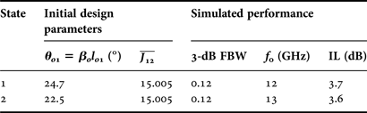
The technology used for the fabrication of the SABs (and the final reconfigurable filter) consists of an eight-mask surface-micro-machining process, developed by the MEMS group of FBK [Reference Giacomozzi, Mulloni, Colpo, Iannacci, Margesin and Faes6]. Figure 9 shows the fabrication process flow. First, an insulating layer consisting of 1 µm of silicon oxide is grown by wet thermal oxidation. The DC-actuation pads, bias lines, and contact bumps (dimples) are defined using a high-resistivity polysilicon layer with a thickness of 0.63 µm. An insulating layer of 300 nm of SiO2 is deposited by low-pressure chemical vapor deposition (LPCVD) using tetraethyl orthosilicate (TEOS).
Fig. 9. Process flow for ohmic switches (cantilever or bridge type). (a) Thermal oxidation; polysilicon and TEOS deposition and contact opening. (b) Metal deposition and patterning. (c) LTO deposition, vias opening and floating metal deposition. (d) Spacer deposition. (e) Seed layer and first Au “Bridge” electroplating. (f) Second Au “CPW” electroplating and release of suspended structures.
A second lithography step defines the opening for the contacts (Fig. 9(a)). A multi-metal layer (Ti/TiN/Al/Ti/TiN) with the same thickness of polysilicon layer (0.63 µm, in order to avoid non-planarities in the bridge) is used as an underpass to connect signal lines under suspended structures (Fig. 9(b)). Then, a 100-nm-thick SiO2 dielectric layer (low-temperature oxide, LTO) is deposited. The next lithography step defines the vias in the LTO. A 5-nm-Cr–150-nm-Au layer (Fig. 9(c)) is deposited by electron-beam gun to be used as floating metal and to reduce the metal-Au resistance inside the vias. This 150-nm layer defines metal–insulator–metal (MIM) capacitors or ohmic contacts. For the fabrication of suspended movable membranes and air bridges, different thicknesses of photoresist sacrificial layer (spacer) can be used, usually from 1.6 to 3 µm (Fig 9(d)). Two gold layers of different thicknesses can be deposited (electroplated) to define transmission lines and suspended membranes. The movable bridges are manufactured using a 1.8-μm-thick gold layer (Fig. 9(e)), and a second 3.5-μm-thick superimposed gold layer (Fig. 9(f)) is used to increase the rigidity of selected parts of the membranes. To release the suspended structures, the spacer is removed using oxygen plasma.
The RF-MEMS switch proposed in this paper (SAB described in Section III.B) is quite different (regarding membrane shape, suspension type, and the use of two simultaneous ohmic contacts) compared to the ohmic and capacitive RF-MEMS switches described as examples in [Reference Giacomozzi, Mulloni, Colpo, Iannacci, Margesin and Faes6].
B) RF-MEMS SAB
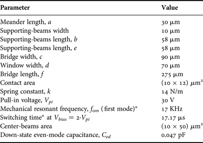
In [Reference Contreras7], a new shunt-type ohmic-contact RF-MEMS SAB was proposed and fabricated, using the integrated RF-MEMS process described above. This bridge-type device could be used in CPW reconfigurable multimodal circuits for a selective use of the CPW odd mode. In this work, an improved version of that SAB, shown in Fig. 10, is used. It has been patterned on a 5-kΩ·cm high-resistivity silicon substrate with a permittivity ε r = 11.9 and thickness h = 200 µm, and features a reinforced gold membrane with two ohmic contacts at the edges (the substrate used in [Reference Contreras7] was quartz). The bridge membrane is anchored to isolated islands by folded-beam suspensions, made of a 1.8-μm-thick, 10-μm-wide single gold layer. The dimensions of the switch are shown in Table 3.
Fig. 10. RF-MEMS SAB.
Table 3. Dimensions and parameters of the RF-MEMS SAB.
*Simulated parameters.
In contrast to the SAB presented in [Reference Contreras7], the lengths of the SAB-folded suspensions are now 10 µm shorter (thus the stiffness constant is higher), and the bridge window is now 10 µm wider (thus the membrane arms in the membrane center part are narrower – 10 µm compared to 15 µm in [Reference Contreras7] – and therefore the even-mode capacitance is now smaller – 47 fF compared to 95 fF in [Reference Contreras7]). When an actuation voltage V bias equal or higher than the pull-in voltage V pi, is applied to the electrodes, the bridge contacts an underpass metal layer, which is connected to the ground planes of the CPW. The SAB has an air-gap of 3 µm and the distance between the membrane and bottom ohmic contacts is 2.7 µm. The measured pull-in voltage is V pi = 30 V, which gives an estimated stiffness constant k = 14 N/m. The first mode mechanical resonant frequency value, f 0m = 17 KHz, was obtained from electro-mechanical analysis performed with ANSYSTM.
The contact resistance of the SAB has a direct impact on the quality factor of the filter in which the device is integrated, and can be decreased by increasing the contact force [Reference Pothier8]. To increase the contact force, a bias voltage higher than the pull-in voltage has been applied. Thus the contact resistance of the SAB is reduced and the contact reliability is enhanced. For a bias voltage twice the pull-in voltage (V bias = 2·V pi = 60 V) a minimal contact resistance R T = 0.9 Ω was measured (see the odd-mode equivalent circuit – shown in Fig. 12 – and discussion below in this section). Another benefit of increasing the bias voltage is to reduce the switching time (t s) that can be estimated using the expression [Reference Rebeiz9]:
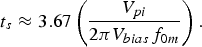 $$t_s \approx 3.67\left({\displaystyle{{V_{pi} } \over {2\pi V_{bias} f_{0m} }}} \right).$$
Thus, applying (1), for a bias voltage V bias = 2·V pi and f 0m = 17 KHz, the estimated switching time is 17.17 µs.
The CPW access circuit to the SAB in Fig. 10 was designed to reduce the inductance of the underpass line connected to the ground planes (which contributes to the total inductance L t of the switch). The CPW access circuit is composed of CPW sections with different dimensions: the outer CPW sections feature 20-μm slots and a 50-μm center strip, resulting in characteristic even- and odd-mode impedances Z 0e1 = 50 Ω and Z 0o1 = 102 Ω, respectively. The inner CPW section features wider 82-μm slots, resulting in characteristic even- and odd-mode impedances Z 0e1 = 78 Ω and Z 0o2 = 118 Ω, respectively.
The RF performance of the SAB with respect to the odd mode was measured using 150-μm-pitch GS-SG probes. Figure 11 shows the measured S 21 parameter for both SAB states, with the outer low-impedance CPW sections de-embedded, and normalized to the inner CPW section odd-mode characteristic impedance Z 0o2 = 118 Ω. The IL of the SAB in the up state is better than 0.65 dB up to 35 GHz, and the isolation in the down state is better than 10 dB up to 30 GHz and better than 14 dB below 15 GHz.
Fig. 11. Measured and simulated S 21 for the up state (IL) and the down state (isolation) of the SAB.
From the measurements in Fig. 11, equivalent circuits for the SAB can easily be derived. Figure 12 shows the SAB equivalent circuit (for the odd mode) in the down state, and the simulated S 21 parameter is also plotted in Fig. 11. For the up state, the odd-mode equivalent circuit model of the SAB is similar to that in Fig. 12, but substituting the series RL circuit by a series RLC one. The capacitance of this series RLC circuit is extremely low (lower than 0.2 fF) since the air gap between the membrane and bottom ohmic contacts is 2.7 µm, and the contact area is small (10 µm × 12 µm), and makes the impedance of the RLC circuit negligible.
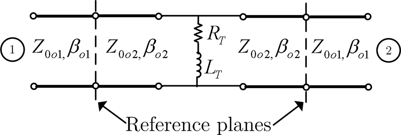
Fig. 12. Equivalent circuit model (for the CPW odd mode) of the SAB and CPW access when the switch is in the down state, R T = 0.9 Ω and L T = 0.12 nH. β o1, β o2 are the odd-mode phase constants.
The even-mode equivalent circuit is a series RLC connected in parallel to the access lines. The behavior of the switch for the even mode was measured using ground-signal-ground probes and it was found that, for the up state, R = 0.2 Ω, L = 0.03 nH, and C = 1 fF. The capacitance in the up state is very low since the air gap between the membrane and the CPW central conductor is 3 µm, the air gap between the membrane and bottom ohmic contacts is 2.7 µm and the contact area is small (10 µm × 12 µm). When the pull-in voltage is applied to the electrodes, the bridge touches the contact areas first, and thus the center beams of the bridge do not remain flat above the underpass. For the down state it was found that R = 0.4 Ω, L = 0.03 nH, and the capacitance (as commented above) is C = 0.047 pF.
Compared to the SAB presented in [Reference Contreras7], this device uses shorter folded-beam suspensions to reduce the area of the switch, and thinner center beams. This means that this SAB has less impact on the CPW even mode, and, in addition, it is more robust against high-power effects, such as self-biasing [Reference Peroulis, Pacheco and Katehi10], because the switch is not connected to the ground planes in the up-state and the odd-mode overlapping RF area is minimal.
IV. FILTER IMPLEMENTATION
Figure 13 shows the second-order bandpass filter with reconfigurable center frequency designed according to the principles and RF-MEMS integrated process described above, with f 01 = 12 GHz (state 1) or f 02 = 13 GHz (state 2). The operating frequencies where chosen to test the upper frequency limits of the performance of the RF-MEMS SABs, which can be considered acceptable up to 15 GHz. Figure 14 shows a close-up of the input MII. Again, the filter was fabricated on a 5-kΩ·cm high-resistivity silicon with permittivity ε r = 11.9 and thickness h = 200 µm. The area of the filter, including bias lines, is 4.97 mm × 0.74 mm.
Fig. 13. Fabricated RF-MEMS frequency-reconfigurable filter using SABs.
Fig. 14. Input MII with an RF-MEMS SAB.
When a bias voltage V bias, higher than V pi, is applied simultaneously to both SABs (input and output), there will be a shift in the center frequency and a change in the input and output couplings [Reference Contreras, Ribó, Pradell and Blondy5].
Table 4 shows the main dimensions of the reconfigurable second-order quarter-wavelength filter. The difference between the length l o1 of state 1 and the one of state 2 is Δl o1 = 140 µm. From Table 4, it is apparent that the ratio l o1/l r changes from l o1/l r = 0.212 for state 1 to l o1/l r = 0.161 for state 2. However, this variation translates into a very small change in the filter FBW between the two states.
Table 4. Dimensions of the frequency-reconfigurable filter.

V. EXPERIMENTAL RESULTS
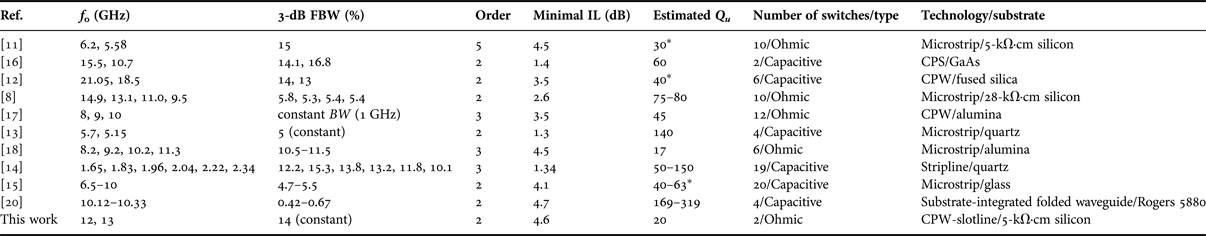
Figures 15(a) and 15(b) compare the measured and simulated responses for both states of the reconfigurable filter. As explained in Section III, the bias voltage applied to the SABs (state 2) was V bias = 2·V pi = 60 V. The measured IL (|S 21|) for both states is lower than 4.7 dB (similar to that reported in [Reference Ocera, Farinelli, Mezzanotte, Sorrentino, Margesin and Giacomozzi11] for a planar filter fabricated on a 5-kΩ·cm high-resistivity silicon substrate), which corresponds to an estimated unloaded quality factor Q u = 20. The lower resistivity of the substrate (compared to alumina, quartz or GaAs) in addition to metallization conductivity can justify the low-unloaded quality factor, as explained in [Reference Pothier8]. The unloaded quality factor can be improved using higher resistivity substrates such as quartz [Reference Fourn12–Reference Entesari and Rebeiz15], GaAs [Reference Nordquist16], Alumina [Reference Chan, Fouladi, Ramer and Mansour17, Reference Nordquist18], or a silicon substrate with higher resistivity [Reference Pothier8]. The filter IL could also be reduced by increasing the width of the slotline resonators (thus increasing the slot width-to-substrate thickness ratio) [Reference Wolff19]. In our design a relatively small ratio (90 µm/200 µm = 0.45) has been used. A higher ratio would probably decrease the slotline loss but at the expense of a higher dispersion [Reference Wolff19], which is not an optimal solution for filters with reconfigurable center frequency and constant FBW. Another approach to reduce the IL (thus increasing the unloaded quality factor) is to combine planar technologies and waveguides [Reference Rebeiz1, Reference Scarbrough, Goldsmith, Papapolymerou and Yuan20]. In [Reference Scarbrough, Goldsmith, Papapolymerou and Yuan20], an RF-MEMS tunable filter using substrate-integrated folded waveguide technology was presented, achieving a high Q u (ranging from 169 to 319), for a tuning range 10.12–10.33 GHz using 4 RF-MEMS capacitive switches in a hybrid assembly.
Fig. 15. (a) Narrow-band comparison between the measured S parameters of the frequency-reconfigurable filter and those predicted by its circuit model. (b) Wideband comparison. In both cases, black traces correspond to state 1, and grey ones to state 2.
The measured FBW is only 0.02 higher than expected by the circuit simulation, but the same 3-dB FBW is maintained in both states as anticipated. The difference (1 dB) between the simulated and measured IL levels are due to a lower substrate resistivity in certain areas of the wafer (less than 5-kΩ·cm).
As shown in Fig. 15(b), the wideband response of the circuit simulation is in good agreement with the measurements, validating thus the multimodal circuit model for the filter. The small discrepancies above 30 GHz are attributed to the modeling of the capacitive coupling (performed at f 02), which ceases to be accurate above this frequency.
Table 5 presents a comparison between the switchable filter presented in this work and other RF-MEMS switchable filters available in the literature [Reference Pothier8, Reference Ocera, Farinelli, Mezzanotte, Sorrentino, Margesin and Giacomozzi11–Reference Nordquist18, Reference Scarbrough, Goldsmith, Papapolymerou and Yuan20]. Indeed, the unloaded quality factor can be improved using high-resistivity substrates [Reference Pothier8, Reference Fourn12–Reference Nordquist18] or substrate-integrated folded waveguide technology [Reference Scarbrough, Goldsmith, Papapolymerou and Yuan20] (although more bulky, the latter exhibits the highest quality factor reported). The uniplanar filter here proposed is very compact (4.97 mm × 0.74 mm), and uses only two integrated RF-MEMS switches to shift upwards its center frequency (8.33% shift) while maintaining the same FBW. This type of filter topology can be used in combination with varactor-loaded resonators [Reference Contreras, Ribó, Pradell and Blondy5] to expand downwards the operation frequency range.
Table 5. Performance of selected RF-MEMS reconfigurable planar bandpass filters.
*Estimation from reported filter measurements.
VI. CONCLUSION
An RF-MEMS frequency-reconfigurable second-order quarter-wavelength bandpass filter, featuring constant 3-dB FBW for both frequency states, was designed, fabricated, and measured. The filter uses MIIs, which are reconfigured using improved RF-MEMS SABs, which change both the inverter constants and the physical slotline-resonator lengths. The filter can be modeled and designed using the multimodal theory, and the circuit models derived from it. In particular, a multimodal circuit was used to model the inverters and to parametrically investigate the appropriate position for the SABs. The measured IL of the reconfigurable filter is better than 4.7 dB for both states. The unloaded quality factor of the resonators can be improved using higher resistivity substrates or substrate-integrated folded waveguide technology.
The proposed uniplanar filter has a small area (4.97 mm × 0.74 mm), and uses only 2 RF-MEMS switches to shift upwards its center frequency maintaining the same FBW. In this filter topology, varactor-loaded resonators could be used to expand downwards the operation frequency range.
The RF-MEMS SABs are not connected to the ground planes in the up-state and the odd-mode overlapping RF area is minimal, thus they are highly immune to self-actuation. Therefore the filter can support high-input power levels (not accounting for thermal issues, which may cause problems before high-power levels are reached [Reference Peroulis, Pacheco and Katehi10]).
To the authors' knowledge, a frequency-reconfigurable multimodal filter using RF-MEMS SABs has been demonstrated in this work for the first time. It is an example of how the additional degrees of freedom that multimodal CPW circuits offer (as compared to classical monomodal CPW topologies) can be used to develop new topologies of circuits, such as reconfigurable filters.
ACKNOWLEDGEMENT
This work has been founded by research project TEC2010-20318-C02/TCM and the fellowship BES-2008-004923 from the Spanish Ministry of Science and Innovation.
 Adrián Contreras received the B.Eng. degree in Electronics and Communication Engineering from the Universidad de Guadalajara, Guadalajara, Mexico, in 2004, the M.Sc. degree in Electronic and Telecommunication Engineering from the CICESE Research Center, Ensenada, Baja California, Mexico, in 2009, and the Ph.D. degree in Telecommunication Engineering from the Universitat Politècnica de Catalunya (UPC), Barcelona, Spain, in 2013. His current research interests are RF and microwave filters, multimodal circuits, tunable and reconfigurable circuits, and RF-MEMS devices. He is a member of the European Microwave Association (EuMA).
Jasmina Casals-Terré received the M.S. degree in Mechanical Engineering from the Technical University of Catalonia (UPC), Terrassa, Spain, in 2000, and the M.S. degree in Mechanical and Aerospace Engineering from the University of California, Irvine, in 2002. She received her Ph.D. degree in Mechanical Engineering in 2007. Since then, she is working as Associate Professor at Universitat Politècnica de Catalunya (UPC). Her research interests are in bistable MEMS, such as RF switches or microfluidic devices.
Lluís Pradell received the Telecommunication Engineering degree and his Ph.D. degree in Telecommunication Engineering from the Universitat Politècnica de Catalunya (UPC), Barcelona, Catalonia, Spain, in 1981 and 1989, respectively. From 1981 to 1985, he was with Mier-Allende, Barcelona, Spain, as an RF and Microwave Engineer. In 1985, he joined the faculty of UPC, and became a Full Professor in 2005. His research topics include on-wafer measurement and calibration techniques, millimeter-wave systems, multimodal models for CPW structures/transitions, and RF-MEMS devices/applications. Dr. Pradell is a member of the European Microwave Association (EuMA) and the Automatic RF Techniques Group (ARFTG).
Flavio Giacomozzi graduated in Mechanical Engineering at the University of Padova in 1982. Since 1983, he has been working at Fondazione Bruno Kessler, FBK (former ITC-IRST), Trento, Italy. From 1983 to 1988, he worked on the improvements of surfaces properties of materials. Since 1988, he has been with the Materials and Microsystems Division, where he was in charge of the development of fabrication processes. Since 1996, he has been working on MEMS technologies and the realization of prototypes of several devices as sensors and microphones. Currently, he is involved mainly in the development and the fabrication of RF MEMS devices.
Jacopo Iannacci is a researcher in MEMS technology at the Fondazione Bruno Kessler (FBK) in Trento, Italy, where he focuses on (compact) modeling, design, optimization, integration, packaging and testing for reliability of MEMS/RF-MEMS devices and networks for sensors/actuators, energy harvesting, and telecommunication systems. He received the M.Sc. degree in Electronic Engineering (2003) and the Ph.D. in Information Technology (2007) from the ARCES Research Center at the University of Bologna, Italy, and worked as Visiting Researcher (2005–2006) at the DIMES Technology Center of the Technical University of Delft, the Netherlands, on development of packaging and integration solutions for RF-MEMS devices. Jacopo Iannacci authored and co-authored numerous scientific contributions for international journals and conference proceedings, as well as books and several book chapters in the field of MEMS and RF-MEMS technology.
 Miquel Ribó was born in La Seu d'Urgell, Catalonia, Spain, in 1970. He received the Telecommunication Engineering degree from the Universitat Politècnica de Catalunya (UPC), Barcelona, Catalonia, Spain, in 1994, and the Ph.D. degree in Electronics Engineering from La Salle – Ramon Llull University (URL), Barcelona, Spain, in 2001. In 1997, he joined the Communications and Electromagnetics Research Group (GRECO), La Salle – Ramon Llull University (URL), where he currently teaches microwaves and electromagnetic theory. His research interests include the multimodal analysis of coplanar and microstrip transitions, and of electromagnetic compatibility (EMC) problems such as interference generation, propagation, and mitigation. Dr. Ribó is currently Vice-chairman of the Spanish IEEE EMC Society Chapter.