


I. INTRODUCTION
Absorption loss limits the application of conventional microwave waveguides at high-frequency bands. The absorption loss of a microstrip (MS) or coplanar waveguide (CPW) increases by increasing frequency; thus, these types of waveguides are not suitable for high-frequency applications [Reference Ponchak, Narjomenos and Katehi1–Reference Frankel, Gupta, Valdmanis and Mourou5]. Although some other waveguides such as rectangular waveguide (RWG) have an absorption loss less than MS and CPW, still their losses are not desirable at high frequencies [Reference Mortazy, Zhang and Wu6, Reference Yang and Fathy7]. Generally, the presence of metal at the structure of these conventional waveguides brings a high value of ohmic/conductor loss especially while operating frequency increases. One of the proposed solutions to decrease the ohmic loss especially in high-frequency regime is using a dielectric in the middle of two metallic plates, called non-radiative dielectric (NRD) guide, which concentrates the dominant mode in the middle of this waveguide [Reference Kuroki, Ohta and Yoneyama8]. However, the difficulty of the fundamental mode excitation of NRD by conventional planar waveguides is a limitation that makes it barely integrable with other microwave components [Reference Pathak, Koul and Basu9]. A better solution to diminish the total waveguide loss at high frequency is to design a waveguide only made of dielectrics. Recently, a porous dielectric fiber with a core composed of a hexagonal array of sub-wavelength air holes has been proposed at THz [Reference Wiederhecker10–Reference Hassani, Dupuis and Skorobogatiy12]. In this waveguide, the propagating electromagnetic power is confined inside of fiber air gaps providing very low-loss transmission. Although, the general design concept of this porous waveguide can be applied to propose a new generation of low-loss dielectric waveguide for microwave applications, the non-planarity of this porous fiber limits its integrability to conventional microwave components. This integrability limitation comes from the fact that the transition behavior of most microwave waveguides to circular-shape waveguides has an undesirable return and insertion loss comparing to the rectangular-shape waveguides. Furthermore, the fabrication of a porous dielectric fiber containing several air holes is more challenging than a rectangular-shape waveguide. In this paper, we propose the design of a novel low-loss dielectric waveguide operating at microwave frequencies. In the following, we firstly describe the waveguide structure and guiding mechanism of the multilayer porous waveguide (MPW) waveguide. Then, after presenting several designs for MPW waveguides and their characteristics, we compare one of the MPWs with one of the low-loss traditional waveguides already used in microwave. finite difference time domain (FDTD) is the method of our choice for the all simulations in this paper; however, we confirm our result with Ansoft commercial finite element mode solver [13, 14].
II. MPW WAVEGUIDE STRUCTURE
Our proposed waveguide is composed of the periodically arranged rectangular subwavelength air gaps surrounded by dielectric substrates. Figure 1 shows the schematic of this rectangular porous dielectric waveguide with several substrates running along the waveguide, which we name MPW.

Fig. 1. The 3D schematic of our proposed MPW; H g: gap layer thickness, H s: substrate layer thickness, W: waveguide width; L: waveguide length.
In spite of the guiding mechanism in RWG, which is based on lossy reflection of microwave field from metallic surrounded parts, MPW operates based on total internal refraction at air–dielectric interfaces. To satisfy electromagnetic boundary conditions, the displacement field component normal to the interfaces of air and substrates must be continuous, i.e.
where E air, E dielectric, ɛair, and ɛdielectric are the electrical fields in air and dielectric and the dielectric constants of air and dielectric, respectively. Large difference between the permittivity of the air and dielectric substrate causes strong discontinuity in the electrical field amplitude at the air–dielectric boundary, resulting in a high electric field confinement in the air gaps. The sizes of the air gaps and the index and thicknesses of substrate can be optimized to maximize the confinement of microwave power in the air gaps, resulting in a very low absorption loss for MPW. Moreover, the number of layers and the size of cross-section of this waveguides can be optimized to operate in single mode or multimode regime.
III. MPW DESIGN AND CHARACTERISTICS
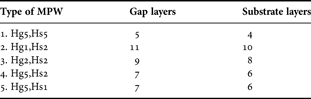
In Fig. 2, the absorption loss and effective index of the first TE and TM modes for five different MPW structures are presented. The width and height of all five MPWs are 10.7 and 4.3 mm to be comparable with the standard K-band waveguide, which is WR42. In all cases, according to the thickness of chosen standard substrates, the number of air gap and substrate layers is changed to reach the height of 4.3 mm.
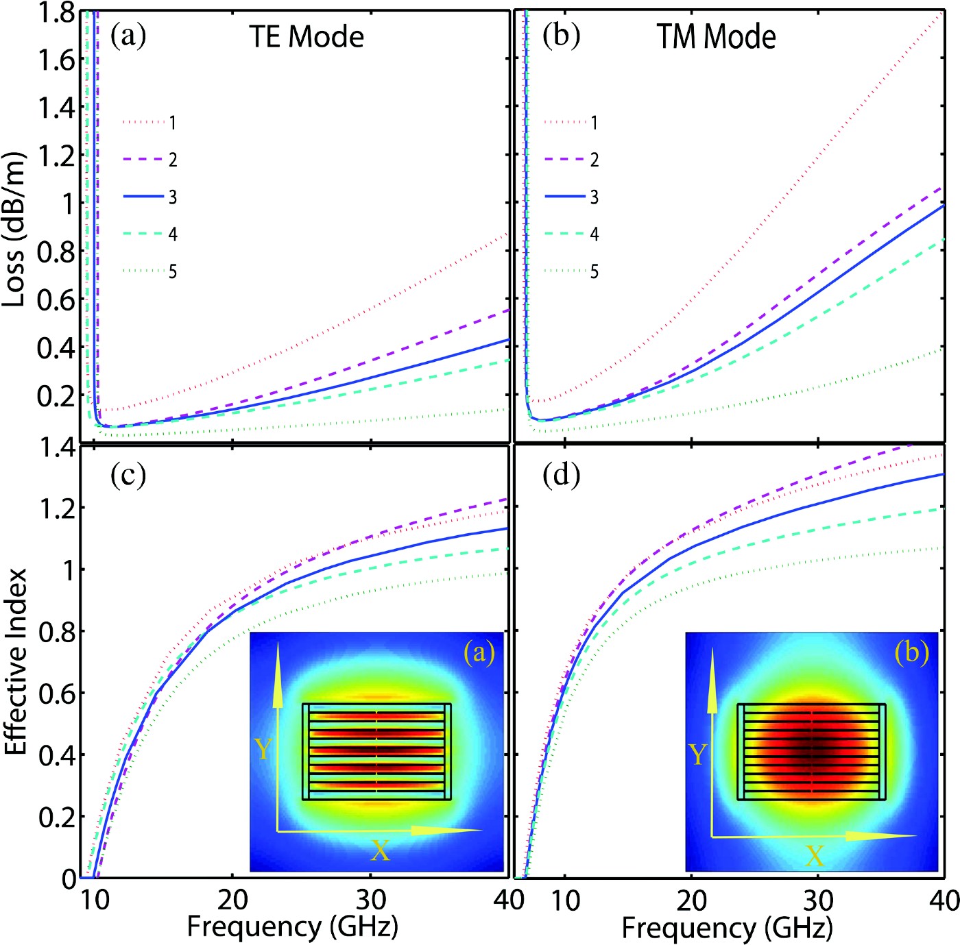
Fig. 2. The absorption loss and effective index of TM and TE modes for the five different MPW structures featured in Table 1; and curves 1, 2, 3, 4, and 5 are corresponding to the MPWs 1, 2, 3, 4, and 5 in this table.
The number of substrate layers and air gaps are indicated in Table 1. The Rogers RT/duroid 5880 is the standard substrate of our choice for all cases with the permittivity of 2.2 and dielectric loss tangent of 0.0009. Hs1/Hg1, Hs2/Hg2, and Hs5/Hg5 stand for the substrate/gap thicknesses of 0.127, 0.254, and 0.508 mm, respectively.
Table 1. The number of substrates and air-gap layers for the designed MPWs.
FDTD is the method of our choice to simulate and optimize the MPW waveguides here. FDTD, a time-domain multipurpose numerical technique, is used to solve Maxwell's equations. Since FDTD uses a broadband pulse as a source, the guiding response of the MPW waveguides over a wide range of frequencies can be obtained by running one simulation. To preform the simulation, first computational domain should be specified, and the material of each cell within the computational domain have to be defined. For our case, the material is either air or dielectric, defined by ɛ air and ɛ dielectric, respectively. Then, we specify a perfectly matched layer (PML) as a boundary condition and a source for our simulation, which can be an impinging plane wave. Since our simulation is an open-region FDTD problem, the PML formulations that technically work as an absorbing region for evanescent waves can considerably suppress the reflection from the boundary area of the simulation.
Figures 2(a) and 2(b) present the absorption losses of the first TE and TM modes for these waveguides. We characterize the modal absorption loss of the MPW waveguides by using the perturbation theory, which can be described by [Reference Snyder and Love15]
![{\rm \alpha} _{wg}={\rm \alpha} _{mat} \left[{\displaystyle{{\sqrt {{\varepsilon} _0 /{\mu} _0 } \vint\nolimits_{dielectric} \, n_r {\vert E}\vert ^2 \, dA} \over {Re\lcub \vint\nolimits_{total} \, {\vec E} \times \mathop {\vec H}\nolimits^{\ast} \cdot\; {\hat z} \, dA\rcub }}} \right]. \eqno\lpar 2\rpar](https://static.cambridge.org/binary/version/id/urn:cambridge.org:id:binary:20151022075450975-0612:S1759078711000596_eqn2.gif?pub-status=live)
where αwg is a modal propagation loss due to material absorption, while αmat is the bulk absorption loss of the dielectric. ![]() and
and ![]() are, respectively, the electric and magnetic fields of the MPW waveguide, while n r is a real part of the refractive index of the dielectric. The absorption loss decreases with increasing the air-gap thickness for the MPWs having the same substrate thickness (Cases 2, 3, and 4 in Figs 2(a) and 2(b) referring to the corresponding MPWs in Table 1). It is worth mentioning that the maximum size of air gaps in these designs are optimized for maximum field confinement. Thus, the field confinements in the air gaps decrease if the size of the optimized air gaps increase further (the results are not shown here). An intuitive study to design an optimum air-gap for maximum field confinement can be found at [Reference Nagel, Marchewka and Kurz16]. On the other hand, the absorption loss decreases, while the substrate thickness decreases in the MPWs having the same air-gap thickness (Cases 1, 4, and 5 in Figs 2(a) and 2(b) referring to corresponding MPWs in Table 1). This is because of the fact that with the thicker substrate the portion of the absorbent dielectric material in the cross section of waveguide increases, resulting in higher absorption losses in the MPW waveguides. Furthermore, our simulation shows that the effect of a change in substrate thickness on both TE and TM microwave losses is more than the effect of a change in air-gap thickness.
are, respectively, the electric and magnetic fields of the MPW waveguide, while n r is a real part of the refractive index of the dielectric. The absorption loss decreases with increasing the air-gap thickness for the MPWs having the same substrate thickness (Cases 2, 3, and 4 in Figs 2(a) and 2(b) referring to the corresponding MPWs in Table 1). It is worth mentioning that the maximum size of air gaps in these designs are optimized for maximum field confinement. Thus, the field confinements in the air gaps decrease if the size of the optimized air gaps increase further (the results are not shown here). An intuitive study to design an optimum air-gap for maximum field confinement can be found at [Reference Nagel, Marchewka and Kurz16]. On the other hand, the absorption loss decreases, while the substrate thickness decreases in the MPWs having the same air-gap thickness (Cases 1, 4, and 5 in Figs 2(a) and 2(b) referring to corresponding MPWs in Table 1). This is because of the fact that with the thicker substrate the portion of the absorbent dielectric material in the cross section of waveguide increases, resulting in higher absorption losses in the MPW waveguides. Furthermore, our simulation shows that the effect of a change in substrate thickness on both TE and TM microwave losses is more than the effect of a change in air-gap thickness.
For each MPW, the absorption loss of TE mode is about 40% lower than TM mode. This difference can be interpreted by the electric displacement field continuity, D air = D dielectric, at air/dielectric interfaces as we look at the insets (a) and (d) in Fig. 2, where the TM and TE field distributions of the Hg2, Hs2 waveguide at 24 GHz are presented, respectively. The transversal electrical field intensity of TE mode, perpendicular to the substrates, is well concentrated in the air gaps, because the continuity of the electric displacement field ɛairE airy = ɛdielectricE dielectricy satisfied at the y direction where the gap size is optimized for maximum confinement. For the TM mode, the continuity of the electric displacement field ɛairE airx = ɛdielectricE dielectricx satisfied at the x direction, where the air-gap size is too big to be able to confine the field, thus the intensity of electrical transverse field of the TM mode in substrate and gap layers is almost the same, and thus the absorption loss is higher.
Figures 2(c) and 2(d) show the effective permittivity of TM and TE modes for the MPWs, respectively. In all designs, the TE modes that are perpendicular to the horizontal substrates are more confined in the air gap region, resulting in lower effective permittivity in comparison with the TM modes. In all designs, the TM and TE cut-off frequencies are almost independent to the number and thickness of the substrates and air-gap layers, and the TM mode is the fundamental mode with lower cut-off frequency. It is obvious that the effective permittivity of both polarizations (TE and TM) increases while air-gap thickness decreases in constant substrate thickness (Cases 4, 3, and 2 in Table 1) or substrate thickness increases in constant air-gap thickness (Cases 5, 4, and 1 in Table 1), as it is shown in Figs 2(c) and 2(d).
It is very useful to compare the loss of our proposed MPW waveguide with the conventional ones operating in the same frequency range. Figure 3 shows a comparison between the losses of two dominant modes of the proposed MPW (Hg5, Hs1) with the dominant mode losses of other four conventional waveguides (the dominant modes are quasi-TEM mode for CPW and MS, and TE 10 mode for RWG and WR42) in K-band frequency range. The substrate type for the CPW, MS, and RWG waveguides is RT/duroid 5880. The CPW has the substrate thickness of 0.508 mm with the strip and slots width of 0.08 and 0.015 mm, respectively. The strip width and substrate thickness of MS waveguide are 0.37 and 0.508 mm, respectively. The microwave losses of the CPW and MS waveguides are shown in the range of 24 GHz. The microwave losses of the CPW and MS waveguides continuously increase while the operating frequency increases in our simulation. In Fig. 3, we have shown also the loss behavior of the WR42 and designed RWG with 4.3 mm substrate thickness and 6.6 mm waveguide width. Even though RWGs can be designed to have a lower loss than the CPW and MS, because of the absence of radiation loss for a desirable high frequency range, the presence of conductors in these waveguides still makes them lossy. Therefore, a fully dielectric waveguide without any conductor, the proposed MPW, is more desirable to diminish the waveguide loss considerably. The losses of the two dominant modes of the MPW are illustrated in Fig. 3. The propagating electrical field of the TE mode of this MPW is highly confined between the air gaps, resulting in a very low-loss propagation regime, compared to that of the TM mode, which is confined at substrates and air gaps (shown in the insets of Fig. 2). Notice that, these losses of TM and TE modes of the MPW are significantly less than even that of the RWG and WR42 waveguides. Moreover, the TE field distribution of MPW is more similar to that of the TE 10 mode of RWG as well as quasi-TEM mode of MS/CPW. This similarity makes MPW more conveniently integratable with these conventional waveguides. In addition to the low-loss guidance mechanism of the MPWs, in fact, it is a low-loss artificial material with adjustable refractive index that can be made of any available commercial dielectric regardless of its index value. For example, to have an enhanced filled RWG with lower loss and desirable dielectric index, we propose to use an MPW inside of a RWG instead of a real dielectric. This structure can be the proposed MPW (Hg2, Hs2) surrounded with a RWG which makes an artificial filled RWG with the dielectric permittivity of 1.56. This artificial dielectric permittivity is obtained from the average index value of the gap and substrate permittivity, where the nine substrates with the permittivity of 2.2 in Hg2, Hs2 occupy the 52.9% of the MPW cross section.

Fig. 3. The comparison of absorption losses for different waveguides including CPW, MS, RWG, WR42, and the TM/TE mode of the Hg2, Hs2 MPW.
In Fig. 4, the loss of the RWG filled with MPW is compared with a RWG filled with an imaginary material having the same permittivity of MPW (1.56) and substrate loss tangent of 0.00048 which is 52.9% of the loss tangent of RT/Duroid 5880. The widths and height of both waveguides are 10.7 and 4.3 mm, respectively. Although, the almost equal cut-off frequency of both waveguides, 12 GHz, shows that the material permittivity inside RWGs is almost identical; the presence of the sub-wavelength air gaps in the MPW lowers the loss about two times. In addition to the lower loss guidance, the presence of the EM fields in the air gaps causes to lower the effective permittivity of the waveguide as frequency increases. Consequently, this concept can be generalized to make a low-loss artificial material with permittivity of choice for the microwave waveguides.
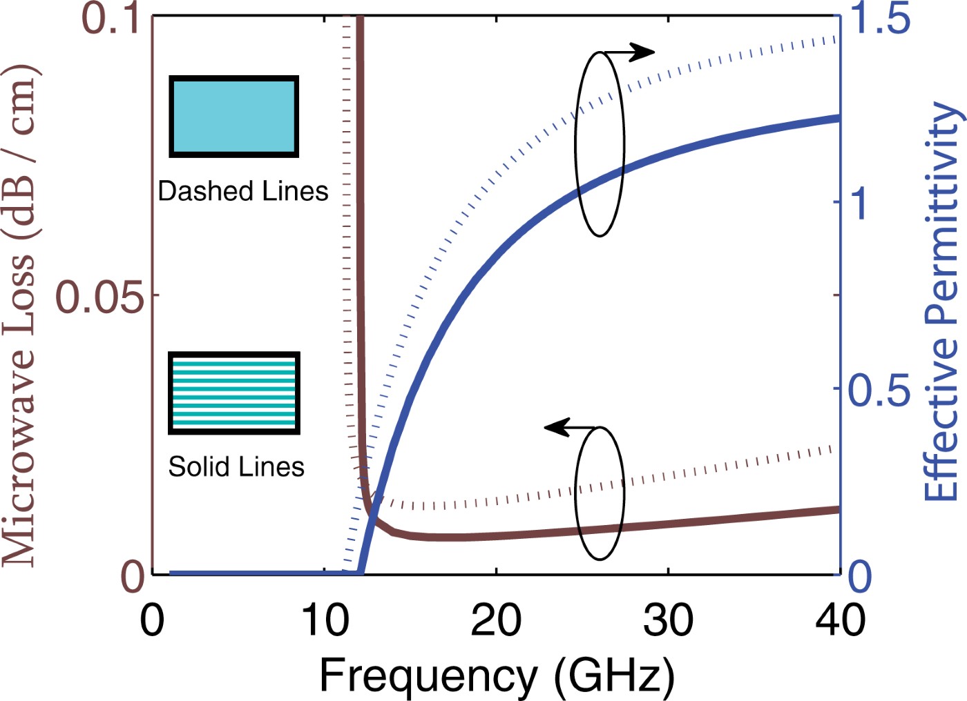
Fig. 4. The absorption loss and effective index of RWG and also MPW filled RWG. Solid lines for RWG filled with MPW and dot-lines for RWG filled with imaginary material having the index of 1.56.
IV. CONCLUSION
In conclusion, the design of a novel MPW have been introduced. Absorption loss analysis of the MPW shows that the loss of this waveguide, only composed of dielectrics, is less than that of the any other conventional microwave waveguides, usually composed of dielectrics and metals. Furthermore, we have illustrated that the transverse electric field of the MPW is considerably confined in the air gaps, resulting in low-loss transmission for the TE mode. On the other hand, even though the transverse magnetic field is less confined in the air, the loss of TM mode is still less than that of a low-loss RWG. Finally, the proposed MPW has been considered as an artificial dielectric in the structure of other microwave waveguides to overcome the lack of a low-loss dielectric material with desirable permittivity.
 Ebrahim Mortazy received the B.Sc. degree from Mazandaran University, Babol, Iran, in 1999, the M.Sc. degree from Tarbiat Modares University, Tehran, Iran, in 2001, and the Ph.D. degrees from the Ecole Polytechnique de Montreal, Canada, in 2010, all in electrical engineering. He is currently a postdoctoral research fellow with the Institut National de Recherche Scientifique (INRS), Varennes, QC, Canada. He was a faculty member of Iran Telecommunication Research Center from 2001 to 2005. His research interests are optoelectronics/electro-optics devices, microwave devices, thin-film deposition, optical modulators, photodetectors, terahertz generation and microwave photonics. Dr. Mortazy is a member of Ordre des ingenieurs du Quebec (OIQ).
 Dr Alireza Hassani received his Ph.D. (2009) in Engineering Physics from University of Montreal (Montreal Polytechnic), Montreal, Canada. His Ph.D. was devoted to design of Photonic Crystal based Plasmonic sensors for bio-sensing application as well as design of new generation of THz waveguides, called THz porous waveguides. He is holder of many prestigious Canadian and international awards and fellowships such as: the NSERC (the most prestigious Canadian postdoctoral fellowship), the FQRNT (the most prestigious postdoctoral Fellowship in Quebec province), the prestigious TEN-CIPI from Canadian Institute for Photonics Innovations, the IEEE Lasers and Electro-Optics (LEOS) Graduate Student Fellowship Awards, and the Incubic/Milton Chang grant from CLEO. He is now with the National Institute of Scientific Research (INRS-EMT), one of the national excellent labs of Canada. His current interest is design and commercializing of the photonic devices for health industry, especially photonics lab-on-chip and multiphotons biomicroscopy.
 Dr. François Légaré received his B.Sc. (1998), M.Sc. (2001), and Ph.D. (2004) in Chemistry from the University of Sherbrooke (Canada). His Ph.D. research was on attosecond science and ultrarast molecular imaging. His postdoctoral research was carried out at the Harvard School of Dental Medicine on imaging with nonlinear optical microscopy techniques tissues rich in collagen type-I proteins. He is currently Assistant Professor at INRS-EMT and his research program is focused on developing and using laser technologies and nonlinear optical phenomena for imaging applications in ultrafast molecular science and biology.
 Ke Wu is professor of electrical engineering, and Tier-I Canada Research Chair in RF and millimeter-wave engineering at the Ecole Polytechnique (University of Montréal), Montréal, QC, Canada. He also holds the first Cheung Kong Endowed Chair professorship (visiting) with Southeast University, the first Sir Yue-Kong Pao Chair professorship (visiting) at the Ningbo University, and an honorary professorship at the Nanjing University of Science and Technology and the City University of Hong Kong. He has been the Director of the Poly-Grames Research Center and the founding Director of the Center for Radiofrequency Electronics Research of Quebec (Regroupement stratégique of FRQNT). He has also hold guest and visiting professorship in many universities around the world. He has authored or coauthored over 765 referred papers, and a number of books/book chapters and patents. His current research interests involve substrate integrated circuits (SICs), antenna arrays, advanced CAD and modeling techniques, and development of low-cost RF and millimeter-wave transceivers and sensors for wireless systems and biomedical applications. He is also interested in the modeling and design of microwave photonic circuits and systems. Dr. Wu is a member of Electromagnetics Academy, the Sigma Xi Honorary Society, and the URSI. He has held key positions in and has served on various panels and international committees including the chair of Technical Program Committees, international Steering Committees and international conferences/symposia. In particular, he will be the general chair of the 2012 IEEE MTT-S International Microwave Symposium (IMS). He has served on the editorial/review boards of many technical journals, transactions and letters as well as scientific encyclopedia including editors and guest editors. He is currently the chair of the joint IEEE chapters of MTTS/APS/LEOS in Montréal, QC, Canada. He is an elected IEEE MTT-S AdCom member for 2006–2012 and serves as Chair of the IEEE MTT-S Member and Geographic Activities (MGA) Committee. He was the recipient of many awards and prizes including the first IEEE MTT-S Outstanding Young Engineer Award, the 2004 Fessenden Medal of the IEEE Canada and the 2009 Thomas W. Eadie Medal of the Royal Society of Canada. He is a Fellow of the Canadian Academy of Engineering (CAE) and a Fellow of the Royal Society of Canada (The Canadian Academy of the Sciences and Humanities). He is an IEEE MTT-S Distinguished Microwave Lecturer from Jan. 2009 to Dec. 2011.
 Mohamed Chaker received the Ph.D. degree in plasma physics from the Université de Montréal, Montréal, QC, Canada, in 1986. In 1986, he joined the Institut National de la Recherche Scientifique (INRS), Québec, QC, Canada, where he was involved with laser–matter interaction plasmas and X-ray lithography, initially as a Post-Doctoral Fellow, and, since 1989, as a Professor. In 1993, he became a Full Professor. He has been the Director of the INRS Énergie, Matériaux et Télécommunications Research Center (INRS-EMT), Montréal, QC, Canada between 1999 and 2004, and Director of the Laboratory of Micro and Nanofarication (LMN) of the INRS-EMT since 2004. He is also the Holder of the Canada Research Chair on plasmas applied to micro-and nanofabrication technologies. His current research interests include the characterization of advanced plasma sources (high-density plasmas and laser-produced plasmas) for applications to thin-film synthesis, nanometer pattern transfer, nanoparticles production, and device fabrication.


