


I. INTRODUCTION
DC power is a very limited and expensive resource in space-borne applications. Inside the spacecraft, one of the most demanding equipment in terms of DC power is the radio frequency (RF) high-power amplifier (HPA) that is used to transmit data to ground. In this context, the trends for future services (e.g. telecommunications and earth observation) call for higher data rates and, therefore, the need for higher RF output power for a given allocated bandwidth [Reference Angeletti, Coromina, Deborgies, De Gaudenzi, Ginesi and Vernucci1, Reference Hernández, Krozer, Vidkjær and Dall2]. This condition puts stringent requirements on the thermal management of the platform since the DC power dissipation in the RF power amplifier is also increased. Therefore, highly efficient solid state power amplifiers (SSPAs) are required.
In particular, switched mode power amplifiers (SMPAs) are able to offer high peak efficiency when driven by a constant envelope rectangular input signal by means of RF pulse-width modulation [Reference Colantonio, Giannini and Limiti3, Reference Besslich4].
This paper focuses on the RF pulse-width modulator and driver (PWMD) used to drive the final high-power stage (Fig. 1). The high-power output stage will be realized in a later stage of the project.

Fig. 1. Simplified SMPA transmit chain overview.
The PWMD consists of a pulse-width modulator (PWM) and a driver capable of exciting the large input capacitance of the final high-power stage. In this work, the driver has been designed on the same chip as the PWM to increase the level of integration and avoid unnecessary interfaces that might deteriorate the square shape characteristics of the signal (Fig. 1). The high-power stage output matching network reconstructs the AM information by means of a resonant matching network tuned to the transmit frequency. Several of these chains can be combined at the input and output to achieve higher output power levels and larger dynamic ranges [Reference Ghosh5].
II. TEST CHIP DESIGN
Originally, the designed PWMD is targeted to drive an 80W class-E GaN HPA in P-Band (435 MHz). In particular, the targeted output waveform from the PWMD circuit is a 4Vp-p rectangular pulse with variable duty cycle and picosecond-order rise/fall times. This sharp-edged waveform is able to efficiently switch ON and OFF the device used in the final high-power stage.
The PWMD chip was designed using IHP's 250 nm SiGe BiCMOS SGB25 V_GD process, which is currently being qualified for space applications (maximum allowed values after applying space de-rating: |Vgs| <2.5 V, |Vds| <2.5 V for the MOS and 6.3 V for the LDMOS). The chip consists of a PWM, voltage level shifters and the on-chip driver (CMOS chains P and N, LDMOS inverter; see Fig. 2). The PWM includes four CMOS inverters of gradually increasing size from 20 µm (PMOS) and 5 µm (NMOS) up to 90 µm (PMOS) and 60 µm (NMOS). At the input, the PWM duty cycle is controlled by offsetting the dc-level of the RF signal by means of the AM input signal. The modulator output signal is a PWM pulse train with a high level of Vcc_pre = +1.23 V and a low level of Vss_pre = −1.23 V.

Fig. 2. Overview of RF-PWMD chip in this work.
As the MOS transistors cannot generate a signal with the 4 V amplitude required at the output, the approach described in [Reference Calvillo-Cortes6] was used: two CMOS chains (P and N, voltage swing = 2.425 V operating between Vcc_P = +1.5 V and Vss_P = −0.975 V in the P-path and between Vcc_N = −0.025 V and Vss_N = −2.5 V in the N-path) drive the final LDMOS inverter, which generates the desired output swing. Diode voltage level shifters placed in front of the CMOS chains shift the input signal (±1.23 V) to the required voltage levels of the P and N CMOS chains. The desired output levels are set by the diode bias voltages Vd_p_top, Vd_n_top, Vd_p_bot, and Vd_n_bot.
The number of transistors and their individual sizes as part of the inverters for the CMOS chains were optimized to maximize the duty cycle range of the chip when operating on a passive load of 1.5 Ω and 30 pF, representing the 80 W high-power stage input impedance. This resulted in 12 inverters for the P-path and 11 inverters for the N-path.
As the transistor sizes associated with the MOS inverters become large, e.g. 6.5 mm (PMOS) and 3.61 mm (NMOS) for the largest inverter of the P-path, small inductances as part of the Vcc/Vss lines on- and off-chip cause significant ringing and overshoot: this phenomenon is shown in Fig. 3, which compares the impact of adding 0.1 nH with ideal Vcc/Vss supplies for the largest inverter of the P-path (11) and a smaller inverter (5). This is detrimental to the performance of the chip and can cause hot carrier injection into the gate oxide of the MOS transistors. Therefore, first of all a preliminary smaller test chip was designed using five inverters for the P-path (largest transistor size: 490 µm (PMOS) and 160 µm, NMOS) and 6 inverters for the N-path (largest inverter size 100 µm (PMOS) and 100 µm (NMOS)). The LDMOS inverter size was proportionally decreased to 810 µm (PLDMOS) and 300 µm (NLDMOS). Also, the load was scaled down according to the ratio of the original LDMOS transistor sizes to the reduced LDMOS transistor sizes. Maintaining the load RC low-pass corner frequency at approximately 4 GHz, a default load of 39 Ω and 1 pF resulted. On-chip, the CMOS chain supply voltages have been blocked twice by 5 pF and 10 Ω in series to ground. The LDMOS source voltages have been individually blocked by 5 pF and 10 Ω in series to ground. ESD protection has been applied to all pins.

Fig. 3. Comparison of the output waveforms of the largest P-path inverter 11 (solid line) and inverter 5 (dashed line) when adding 0.1 nH to ideal Vcc/Vss supply voltages.
The chip layout is shown in Fig. 4. The test Printed Circuit Board (PCB) housing the chip is depicted in Fig. 5: it contains 100 pF 0402 size and 15 pF 0201 size surface mount decoupling capacitors for all supply voltages and 0201 load components.

Fig. 4. Realized chip layout.

Fig. 5. Excerpt of the PCB layout showing the position of the SMD components. The chip interface ports for the 3D simulations are highlighted.
III. TEST CHIP MEASUREMENT RESULTS AT 435 MHZ
A) Pulse shape
Measurements of the output waveform were carried out by measuring the output signal of the 5.1 kΩ resistor (see Fig. 5) using the LeCroy 8600 A oscilloscope, having an input impedance of 50 Ω. The measured waveforms were corrected for the resulting voltage division ratio (50/5150). Fig. 6 displays results for two different values of the AM input voltage Vin (0.32 V for 50% duty cycle and 0.7 V for 18% duty cycle). The pulse rise time (20–80%) varies from 70 to 110 ps depending on the realized duty cycle. The fall time is 100 ps in both cases. However, the pulses are rounded and not flat as expected from simulations of the chip structure only (cf. Fig. 3). Therefore, a three-dimensional (3D) electromagnetic simulation of the host PCB has been carried out using Empire XCcelTM and combined with the simulations of the chip. The Surface Mount Device (SMD) components were included in the simulation setup, as shown in Fig. 5. The interface to the chip was realized by placing ports at the bond pads of the PCB. In total, the PCB comprises 52 ports. The bond wire inductances were calculated using formulas given in [Reference Grover7]. On-chip parasitics have been disregarded due to the small-sized transistors. As shown in Fig. 6, the simulation accuracy using this approach is very good.

Fig. 6. Output waveforms of the chip (measured with a load consisting of 39 Ω and 1 pF). Top: duty cycle = 50%, bottom: duty cycle = 18%. Solid lines: measurement, dashed lines: simulation.
As transistor input impedances are mainly capacitive, the output waveforms of the chip have also been tested with increasing capacitive loads. From Fig. 7, it is seen that with 3.3 and 5 pF loads the pulse shape is rectangular, whereas with 10 pF the output pulse shape becomes triangular.

Fig. 7. Measured output waveform of the chip for capacitive loads of 3.3, 5, and 10 pF, duty cycle = 50%.
B) Dynamic range
The dynamic range of the chip has been evaluated using a spectrum analyzer in zero span set to a center frequency of 435 MHz. This way the fundamental frequency component of the RF-PWMD output pulse train is reconstructed. The minimum duty cycle is 18% (Vin = 0.7 V). For larger values of Vin the pulse amplitude becomes unstable. The maximum value is 70% (Vin = 0 V). For Vin = 0.32 V, the duty cycle is 50%. In this case, a maximum dynamic range of 5.3 dB is achieved. For the sake of comparison, 1.8 dB were achieved in [Reference Calvillo-Cortes6], whereas almost 6 dB were achieved in [Reference Walling8]. These values are not sufficient to support common digital modulation schemes with modest AM dynamic range (e.g. 8-PSK or π/4-DQPSK) with required values of the dynamic range in excess of 10 dB. However, using the approach of [Reference Ghosh5] by means of combining several transmit chains the dynamic range can be improved by 6 dB provided that the dynamic range of a PWMD is larger than 3.5 dB.
IV. ENLARGED CHIP DESIGN
As the transistor sizes associated with the targeted enlarged chip aimed at driving an 80 W high-power stage are considerably larger than for the test chip, it was necessary to take into account the on-chip parasitics and the bond wires inductances. Therefore, besides carrying out 3D simulations for the PCB structures, also 3D simulations of the passive on-chip structures were carried out. These were combined with the transistor models of the MOS/LDMOS transistors.
A pre-study investigating the voltage swings of the larger inverters P7–P11, N8–N12, and the final LDMOS inverter when driving the 80 W high-power stage revealed that strong ringing is observed for the largest MOS inverters (P11) with maximum values of the gate–source voltage of up to 5 V. Only when truncating the CMOS chain to P9 and N10 and reducing the LDMOS size to 8.7 mm (PLDMOS) and 3.06 mm (NLDMOS) the maximum ratings of the chip could be complied with. Owing to the smaller LDMOS transistor sizes it was decided to use a smaller high-power stage: a 40 W transistor (UMS CHK040A) was chosen.
For the design of the enlarged chip, the 3D simulations of the CMOS chains were split up into five different simulation setups: P1–P5, P6–P9, N2–N6, N7–N10, and the LDMOS inverter. This was done to limit the number of ports as part of one 3D simulation and hence to minimize the simulation time. Fig. 8 shows the geometry of the P-path setup. The 3D simulation of the smaller inverters (P1–P5) was connected with the simulation of the larger inverters (P6–P9) by means of interface ports. Also, the LDMOS inverter was connected to both the P-path (P6–P9) and N-path (N7–N10) simulations via interface ports.

Fig. 8. Simulation setup P-path chain P6–P9 (left: total simulation setup, right: inverters P6–P9).
The transistor models were inserted with reference to their gate terminals, i.e. for each transistor the 3D simulation setup contains two ports: one gate-source port and one drain–source port. To minimize the total bond wire inductance, the chip is placed inside a cavity. Off-chip, each CMOS chain supply voltage (i.e. Vcc_P, Vss_P, Vcc_N, and Vss_N) is supplied with a 3D simulation of a supply line including four 0201 size blocking capacitors and one 0402 size capacitor. The capacitor values were optimized to minimize the ringing of the on-chip inverter waveforms.
The resulting total chip layout is displayed in Fig. 9. The chip dimensions: 2097 µm × 2083 µm. The modulator, level shifter, and inverter chains P1–P5 and N1–N6 have been re-used from test chip (highlighted by the dashed yellow frames). ESD protection has been applied to all pins. On-chip blocking was applied by capacitors and resistors: CP and CN which are 10 pF and 5 Ω each. For the LDMOS inverter 225 pF have been realized for C_LP and 275 pF for C_LN. CPand CN are referenced to GND, whereas C_LP is referenced to Vss_N and C_LN to Vcc_P, respectively. The number of bond pads was maximized for Vcc_P, Vss_P, Vcc_N, and Vss_N. Experimentally, the waveforms at the gates of the PLDMOS and the NLDMOS transistors can be monitored via Vg_PLDMOS and Vg_NLDMOS (via on-chip 5 kΩ resistors).

Fig. 9. Total chip layout.
As the harmonic balance simulations of the on-chip driver waveforms are time-consuming and convergence is not easily achieved, the investigations have been carried out for the largest inverters only (i.e. P6–P9, N7–N10, and the final LDMOS inverter). This limitation is justified by the fact that the waveform degradation is most severe for the largest inverters (cf. Fig. 3). For this purpose, the P6 and N7 were driven by appropriate square wave pulse sources. The load consists of the CHK040A transistor (Vth = −1.65 V typ., maximum allowed de-rated gate voltage range: −7.5 V– +1.5 V, Cgs = 12 pF). 5 Ω serve to stabilize the final stage at its gate. The final stage is operated in class E. In the simulations an ideal output matching network has been applied (cf. Fig. 10). The shunt capacitance part of a class E design is absorbed in the drain–source capacitance of the power stage. The output matching network was designed for optimum output power and PAE at maximum power. The drain bias voltage is 38 V.

Fig. 10. Class E output matching network: Lload = 7.06 nH, Rload = 17.5 Ω, Cfilter = 2 pF, Lfilter = 67 nH.
The simulations have been carried out with different values of the voltage swing inside the MOS chains. Besides the maximum allowed value of 2.425 V also a reduced level of 1.5 V was considered leaving more room for overshoot and ringing of the voltage waveforms, which cannot be avoided altogether. Fig. 11 displays the simulated time-domain variation of the gate–source voltage for the largest MOS inverter P9 and the final LDMOS inverter. It is evident that the waveforms are well-behaved and the voltage levels are inside the process maximum ratings.
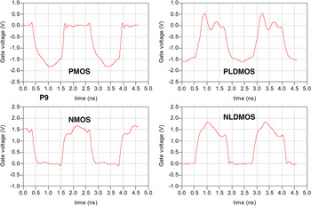
Fig. 11. Gate–source voltage waveforms for largest MOS inverter (P9, left) & LDMOS inverter, right. 1.5 V swing inside MOS chains.
For a duty cycle of 50%, excellent simulated maximum Pout/PAE values are obtained at 435 MHz: 45.6 dBm/83.3% (2.425 V swing), 45.5 dBm/83.5% (1.5 V swing) when driving the class E amplifier with the simulated output waveform of the PWMD. From this it is concluded that the voltage swing inside the MOS chains has little impact of swing on the Pout/PAE performance. The performance has been compared with (a) excitation by means of an ideal PWM pulse (4Vpp, 50% duty cycle, rise time = fall time = 100 ps) and (b) excitation by means of a sinusoidal input signal (4 Vpp). In case of (a) the achievable output power and PAE values are 45.74 dBm and 83.2% and in case of (b) they are 45.45 dBm and 75%. This shows that the PWMD is expected to generate output signals which allow for a significant improvement of PAE compared with a sinusoidal input signal.
V. ENLARGED MEASUREMENT RESULTS WITH PASSIVE LOAD
The test PCB housing the chip is depicted in Fig. 12: for Vcc_P and Vss_N eight 0201 size 100 pF blocking capacitors and two 0402 size 100 pF blocking capacitors have been provided as the peak current consumption which is the largest for these supply voltages. For Vss_P and Vcc_N four 0201 size 100 pF blocking capacitors and one 0402 size 100 pF blocking capacitor are used. For the remaining supply voltages (i.e. Vcc_pre, Vss_pre, VD_p_top, VD_n_top, VD_n_top, and VD_n_bot) only one 0201 size 100 pF and one 0402 size 100 pF capacitor have been provided. This is justified by the reduced current consumption of these voltages. The 5.1 kΩ and 50 Ω transmission lines have been utilized to measure the waveform at the load (RC). Alternatively, when contacting the load C with the 5.1 kΩ resistor the waveform at the capacitor can be measured. This position corresponds to the gate of the power-stage in the final application.

Fig. 12. Enlarged PWMD chip attachment and signal connection.
A) Pulse shape at 435 MHz
Measurements of the enlarged chip have been carried out with a passive load (default load population: 5 or 10 Ω and 12 pF–GND, 0201 size) and 2.425 V swing inside the MOS chains. Significant ringing is observed at load RC for a load of 5 and 12 ΩpF (cf. Fig. 13). The best results are achieved when increasing the resistor value to 10 Ω, using 3 × 30 Ω to realize this value and also using 3 × 4 pF to realize 12 pF. By this measure the parasitic inductance of the load is reduced. Three-dimensional simulations of the PWMD load impedance revealed that the load capacitor together with the PCB track and SMD component inductances cause a resonance at 1.3 GHz which causes the ringing observed in Fig. 13.

Fig. 13. Measured waveforms at the load RC (left) and the load C (right). 2.425 V swing within the MOS chains.
From Fig. 14 it is seen that the simulation accuracy is very good. This demonstrates that the 3D simulation approach chosen to account for the on-chip and PCB parasitics is valid and results in accurate predictions of the PWMD output waveform.

Fig. 14. Left: comparison of simulated (solid) and measured (dotted) voltage wavefoms at load C. Right: dynamic range measurement: 50% duty cycle for Vin = 0.34 V and minimum duty cycle for Vin = 0.71 V.
The measured pulse rise and fall times (20–80%) are 150 ps at the load RC (load: 3 × 30 Ω and 3 × 4 pF). At the load capacitor, which corresponds to the position of the gate of the high-power stage in the final application, the corresponding times are 300 ps (rise), 250 ps (fall).
B) Dynamic range at 435 MHz
Figure 14 shows the waveforms at 50% duty cycle (Vin = 0.34 V) at the minimum realizable duty cycle (22% at Vin = 0.71 V) before waveform collapses. This corresponds to a realizable dynamic range of 4 dB. This is 1.3 dB less than for the test chip. This degradation of the dynamic range is related to the fact that the rise and fall times of the enlarged chip are slightly larger than for the test chip. Still, the dynamic range is sufficient to enlarge the dynamic range as proposed in [Reference Ghosh5]. Other approaches [Reference Özen, Andersson and Eriksson9] aiming at driving final stage devices with output power levels of at least 10 W have realized a slightly higher dynamic range (i.e. 5.5 dB). However, in [Reference Özen, Andersson and Eriksson9] the PWMD modulator and driver only consists of a single inverter, whereas for the work presented here the driver consists of long inverter chains. This approach was chosen to optimize the signal shape whose rise and fall times improve when increasing the number of inverter stages. However, this comes at the risk of pulse swallowing within the inverter chains for small values of the duty cycle.
C) Operating RF frequency range
To test the maximum RF frequency at which the PWMD chip can be operated the RF input frequency was varied; cf. Fig. 15 (50% duty cycle and 2.5 V swing inside MOS chains, load: 3 × 30 Ω and 3 × 4 pF). The PWMD chip can be operated up to 800 MHz. Above that, the pulse train becomes instable (see the 840 MHz curve as part of Fig. 15).

Fig. 15. PWMD chip output waveforms at variable RF frequency.
VI. CONCLUSION
The design and test of an RF-PWM and driver has been described. As small inductances associated with the supply voltage lines of the transistors can have a strong impact on the signal quality and cause considerable ringing. A small test chip was designed and tested at first. It was verified that a simulation approach that combines 3D simulations of the PCB hosting the chip and the active transistor models results in an excellent fit of the simulated response with the measurement data. For the enlarged chip this design approach was extended such that the on-chip parasitics were also included by means of 3D simulations. The enlarged chip can drive a 12 pF load with a 5 Ω stabilization resistor. Owing to the inductance caused by the PCB tracks and the SMD parasitics as part of the load ringing is observed at the PWMD output. This can be improved using three 0201 components per load element and raising the load resistor value from 5 to 10 Ω. The realizable dynamic range is 4 dB. By means of combination of four transmit paths the dynamic range is expected to improve by 6 dB to a total of 10 dB [Reference Ghosh5]. The next step is the test of the enlarged PWMD chip with a 40 W class E amplifier.
ACKNOWLEDGEMENT
This work was supported by the ESA-ESTEC under TRP Contract No. 4000106261.
 Lorena Cabria received the Telecommunications Engineering and the Ph. D. degrees (with and Extraordinary Doctoral Prize) from the University of Cantabria, Santander, Spain, in 2001 and 2007 respectively. Between 2001 and 2011, she worked as a Research Associate in the RF and Microwave Group at the University of Cantabria. Currently, she is working as RF Design Engineer / Project Manager at TTI, Santander, Spain. Her main research interests include RF and microwave integrated circuits, intermodulation distortion control on RF and microwave applications, high efficiency power amplifiers and emerging wireless transmitter architectures.
 Paolo Colantonio was born in Roma, Italy on March 22, 1969. He received the Electronic Engineering degree and Ph.D. degree in Microelectronics and Telecommunications from the University of Roma “Tor Vergata”, Italy, in 1994 and 2000, respectively. In 1999 he became a Research Assistant with the University of Roma “Tor Vergata”, where, since 2002, he has been a Professor of Microwave Electronics. He authored or co-authored more than one hundred and fifty scientific papers. He authored the book High Efficiency RF and Microwave Solid State Power Amplifiers (Wiley, 2009). His main research activities are in the field of nonlinear microwave circuit design methodologies, nonlinear analysis techniques and modelling of microwave active devices.
 Elisa Cipriani received the degree in electronic engineering (M.S.), summa cum laude, in 2007, and the PhD degree in Space Systems and Technology in 2011, from University of Rome Tor Vergata. She is currently a post-doc researcher at Electronic Engineering Department of University of Rome Tor Vergata. Her main research activities concern power amplifiers theory and design, with a focus on high efficiency switching mode power amplifiers and efficiency enhancement architectures. In these fields, she is cooperating with some of the major national and international electronic industries in the design of high power amplifiers for cellular and radar applications. Dr. Cipriani is co-author of many publications presented at international conferences in the field of microwave electronics (EuMW, ISMOT, IMMIC, and MIKON). In 2008 she was awarded the Graduate Research Fellowship sponsored by Gallium Arsenide Application Symposium Association (GAAS) for the paper “Optimization of Class E Power Amplifier Design above Theoretical Maximum Frequency” presented at the European Microwave Integrated Circuits Conference 2008, Amsterdam, The Netherlands.
 Rüdiger Follmann studied electrical engineering at the RWTH Aachen, Germany. In 1994 he joined IMST, where he worked on non-linear device characterization and modelling. After receiving his PhD in 1998 from the University Duisburg, Germany, he became head of the section MMIC design at the IMST, where he developed numerous sensor and radar components. Currently he is Head of the Department RF Circuits and System Integration at IMST.
 Natanael Ayllon received the B.Sc. degree in telecommunications engineering, the M.Sc. degree in electronics engineering and the Dr.-Ing. degree in microwave engineering from the University of the Basque Country (UPV/EHU), Bilbao, Spain, in 2005, 2007 and 2011, respectively. From 2006 to 2011 he was a Research Engineer at UPV/EHU, where he was involved in linear and non-linear stability analysis of microwave circuits, MIC/MMIC design, manufacture and measurement techniques of such circuits. Since 2011, he is with the European Space Agency ESA-ESTEC, where he supports the development of High Power Amplifiers (SSPAs and TWTAs), T/R Modules and future GNSS payloads for space-borne applications.
 Indra Ghosh received the MSc degree in physics from the Unversity of Hamburg in 1192 and the Ph.D. degree in physics from Imperial College, London in 1996. After working with Forschungszentrum Jülich, Philips Research and Siemens mobile in the area of RF solutions for mobile phones he joined IMST in 2007. Here Dr. Ghosh has led numerous industrial projects in the area of mobile and satellite communications. His current position is Director Integrated Solutions.
 Amitabh Chowdhary received his Master's from Indian Institute of Technology, Kanpur in Computational Electromagnetics (Electrodynamics). He worked for Bhabha Atomic research centre and Centre for Advanced Technology in India. He worked on design and implementation of high power radio frequency systems for particle accelerators for 12 years. Later he worked for Philips semiconductors and NXP semiconductors for 10 years, where he has been responsible for Discrete Device design, MMIC design , LDMOS technology characterisation, Application support and product portfolio management. Presently he is working in European space agency as staff member (payload engineer) for last 5 years and has keen interest in GaN technology, High power Discrete devices, MMIC, SSPA, Linearisers related developments. He is also responsible for management of RF product developments related to both active and passive payload products.
 Olaf Kersten was born 1971 in Berlin, Germany. He received his diploma in communication techniques (M.Sc. degree UAS) at the FHTW Berlin in 1997. Since 1998 he has been with IMST in Kamp-Lintfort and is primarily concerned with the development of RF circuits based on GaAs and SiGe. His research interests also include the three dimensional electromagnetic field simulation of antennas and passive RF devices.
 Ulrich Altmann was born in Pretoria South Africa on 9th of November 1971. He received the Dipl.-Ing. degree in Electrical Engineering from the Technical College in Krefeld, Germany in 1998. Since 1999 he has been with IMST, Kamp-Lintfort, Germany. His main work areas include power amplifier design (GaN, CMOS, MMIC-GaAs) and RF systems engineering.


