I. INTRODUCTION
Nowadays, automobile industries demand the usage of communication systems to offer safer and smarter journey. It then buzzes the researchers and manufacturers to design vehicles with navigation and wireless communication systems. Requirements of such communications systems play a crucial role in the selection of antenna module. To address multiple services, planar antennas become the antenna of choice, since they are compact, lightweight, easy to achieve multi-band and cheap. Several solutions have been discussed to get multiband operations with single radiating element [Reference Lee, Hong, Lee, Park and Seong1–Reference Gamage, Engjom and Jensen5]. The antennas discussed in literature are either directional with circular polarized or omnidirectional with linear polarized. But, circularly polarized omnidirectional antenna helps to maintain better communication between moving vehicle [Reference Kenney6, Reference Koch7]. Thus, this research targeted designing an omnidirectional, circularly polarized penta-band planar spiral antenna [Reference Ramya, Rama Rao and Venkataraman8] to resonate at 1.2 and 1.5 GHz (navigational systems), 2.4 and 3.3 GHz (wireless communication systems), and 5.8 GHz (dedicated short range communication system (DSRC)). In general, these vehicle antennas are often connected to its radio receiver via transmission line called the feed line. Any losses in the feedline deeply affect the received signal-to-noise ratio. This feed line loss can be suppressed by integrating antenna with the low noise amplifier (LNA), which delivers necessary gain to compensate the feed line loss [Reference Malayeri9]. By integrating passive antenna with LNA further increases the receiver sensitivity, improves impedance matching [Reference Lin and Ma10], and reduces system size [Reference Valizade, Rezaei and Orouji11].
To address multiband operation, it necessitates design of multiband LNA. The traditional approach to achieve multiband LNA is the use of individual input stage for each operating frequency, resulting in more noise and large form factor. A second approach involves, designing a wideband circuit that covers entire band, amplifies strong unwanted blockers along with the desired frequency bands, resulting in poor receiver sensitivity [Reference Hossein12, Reference Parvizi, Allidina and El-Gamal13]. The third approach is designing a multiband circuit with switches to select one frequency, resulting in only one band operation at a time [Reference Meaamar14, Reference Nozahi, Mohamed, Sinencio and Entesari15]. Thus there is a need for design of a concurrent multiband LNA. A few concurrent multiband LNAs [Reference Phan and Farrell16–Reference Kao, Chiang and Yang21] have been designed in the recent past. However, concurrent multi-band LNAs with more than three bands have been hardly implemented. To overcome the above-mentioned limits, we propose a LNA with simultaneous penta-band reception with good gain and low noise figure (NF). The designed LNA employs frequency transformation methodology for multiband input matching, GaAs pseudomorphic high electron mobility transistors (pHEMT) technology for better noise reduction and simple LC network is designed for simultaneous reception. Finally, the antenna and LNA were co-designed and analyzed.
Further, the paper is organized as follows, Section II defines the design of the passive antenna and its performance analysis followed by Section III, discusses on design of concurrent penta-band LNA and its performance analysis followed by analysis of integrated antenna with LNA.
II. DESIGN AND ANALYSIS OF PASSIVE ANTENNA
A) Design principle
The microstrip is a good candidate for on-board integrated antenna, due to its compact structure, light weight, easy to achieve multi-band. We have chosen planar spiral structure, since this structure allows maximum current flow in the conducting element, thereby helps to minimize the antenna dimension. The antenna has been designed considering (a) resonant frequencies 1.2, 1.5, 2.4, 3.3, and 5.8 GHz (b) omnidirectional radiation pattern with circular polarization. In the proposed design, the arm radius decides the operating frequency. We have taken the arms radius as λg/8π. The inner and outer arm radius (R 1 and R 2) are calculated based on the upper and lower center frequencies, respectively, using equations (1) and (2) and the width of the spiral for N turns is calculated using equation (3). Figure 1 [Reference Ramya, Rama Rao and Venkataraman8] shows geometry of the passive antenna with dimensions.
 $$R_1 =\, \displaystyle{C \over {8\pi f_h}}, $$
 $$R_2 =\, \displaystyle{C \over {8\pi f_l}}, $$
 $$S =\, \displaystyle{{R_2 - R_1} \over {4N}}.$$

Fig. 1. Prototype of the passive antenna [Reference Ramya, Rama Rao and Venkataraman8].
B) Results and discussions
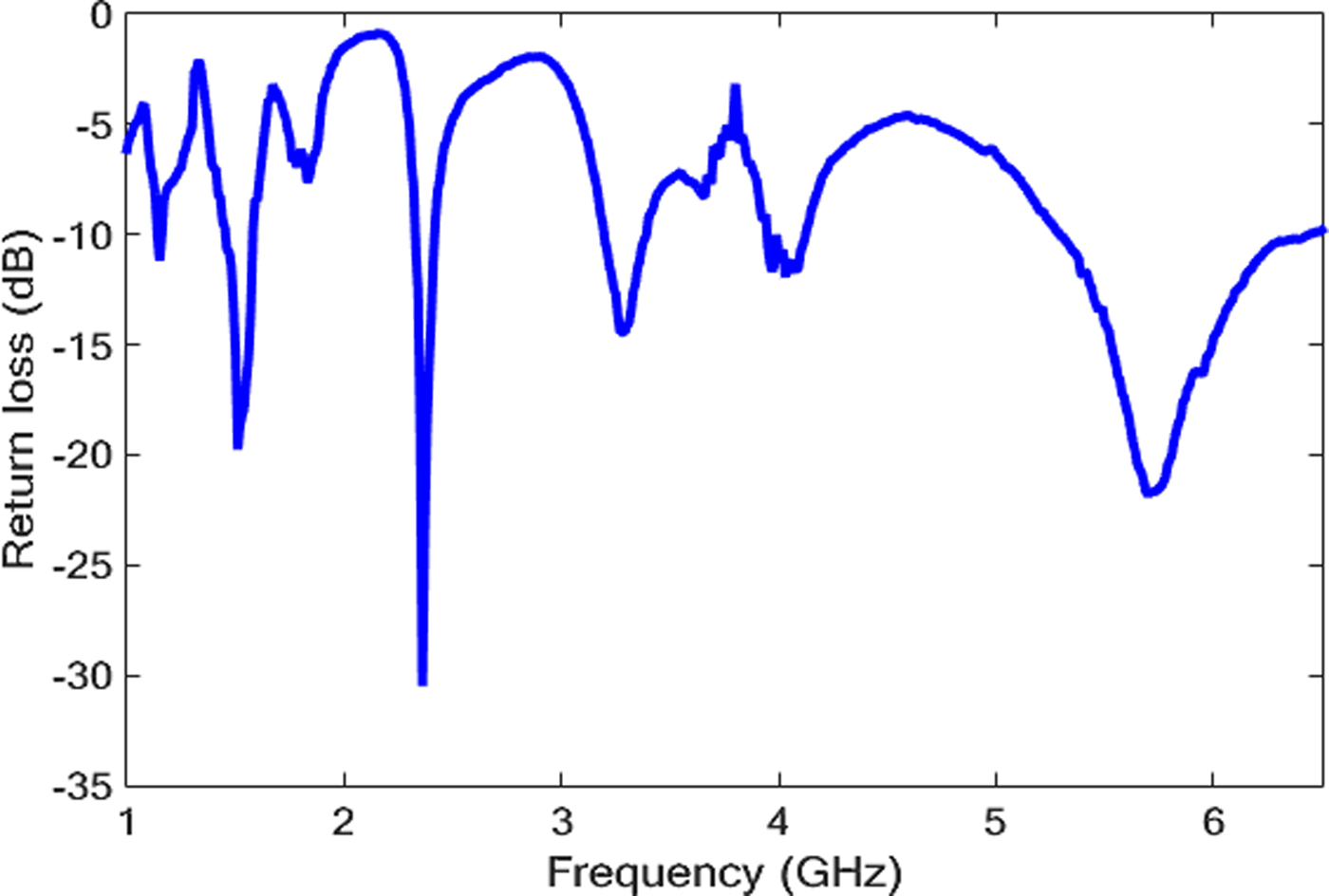
The antenna is printed on 1.57 mm thickness FR4- Epoxy substrate with the ε r = 4.4, and loss tangent (δ) = 0.02. The Keysight's N9926A Vector Network Analyzer is used to validate the antenna performances. Figure 2 shows the measured return loss of the passive antenna. According to the result, the proposed passive antenna has five resonances operating on 1.2, 1.5, 2.4, 3.3, and 5.8 GHz frequencies.

Fig. 2. Return loss of the passive antenna.
The far field measurement has been carried out using SG 64. It is a standalone antenna measurement with CTIA certifiable measurement facilities. Figure 3 shows measured E- and H-plane of the passive antenna. It shows antenna has broadside radiation pattern at desired frequencies.
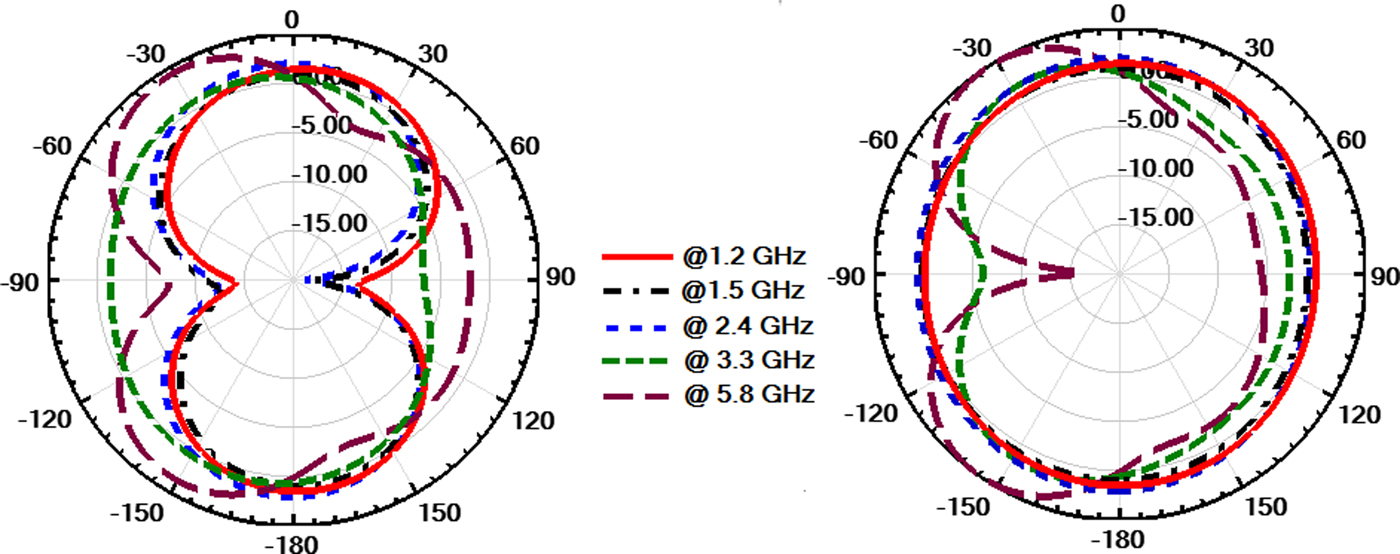
Fig. 3. E- plane and H-plane pattern of the passive antenna.
III. DESIGN AND ANALYSIS OF CONCURRENT LNA
A) Design principle
The LNA design is one of the key building blocks in communication systems. The four essential parameters in design are gain, NF, linearity, and impedance matching. As a designer, we should minimize the additional noise by allowing trade-offs, which include impedance matching, picking the proper amplifier technology, and selecting low-noise biasing conditions. Further targets to be considered are the LNA's operating bandwidth, gain flatness, stability, input, and output voltage standing wave ratio.
1) BIASING CIRCUIT
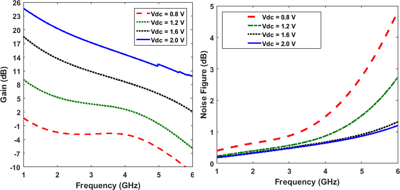
The choice of active device is the prime step in amplifier design. The bipolar junction transistor was the first active element to provide practical gain and NF at microwave frequencies. Later, the development of field-effect transistors (e.g., GaAs MESFET) provides high gain and lower NF than bipolar transistors for the higher frequencies. Currently, high-electron-mobility transistors, such as pHEMT compete for low NF and high gain at high frequencies (up to 100 GHZ) and it allows better trade-off between high linearity and low NF than bipolar junction transistors [Reference Ludwig22]. In addition, circuit topology is an important concern, which encompasses issues such as gain and impedance matching. A common source topology with inductive degeneration [Reference Shaeffer and Lee23] is used in our design. The degeneration inductance L2 ensures simplified input matching by suppressing the susceptance, thus providing better impedance and noise matching. Further, a bypass capacitor C1 is added to isolate the influences from dc power supplies and connected cables. Finally, a proper DC bias needs to be set to achieve good gain and unconditional stability over the entire frequency band. The gain and NF performances of the amplifier are analyzed by varying the bias voltage from 0.8 to 2 V. Figure 4 shows the gain and NF under different bias conditions. The proposed amplifier bias voltage is set to 2 V, since it provides good gain and linear variation over the desired bands. Also, the circuit draws 60 mA from the 2 V supply.

Fig. 4. Effects of DC biasing on Gain and NF.
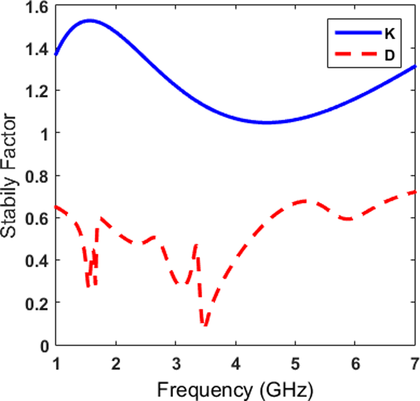
Further, the stability of an amplifier is determined using the Rollet's stability factor, K is defined as in equation (4).
 $$K =\,\displaystyle{{1 - {\rm \;} \left \vert {S_{11}} \right \vert ^2 - {\rm \;} \left \vert {S_{22}} \right \vert ^2 - {\rm \;} \left \vert \Delta \right \vert ^2} \over {2{\rm \;} \left \vert {S_{12} S_{21}} \right \vert}}, $$
where Δ = |S 11 S 22 S 12 S 21|, in addition to the auxiliary stability factor D can be defined as in equation (5).
 $$D = 1 + {\rm \;} \left \vert {S_{11}} \right \vert ^2 - {\rm \;} \left \vert {S_{22}} \right \vert ^2 - \left \vert \Delta \right \vert ^2. $$
For unconditional stability, K > 1 and D > 0 [Reference Ludwig22]. Figure 5 shows the value of K and D of the designed amplifier, which proves the unconditional stability over the entire band.

Fig. 5. Stability analysis of the proposed LNA.
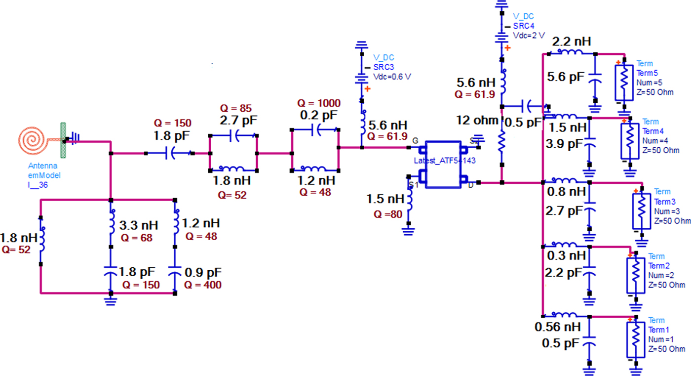
Figure 6 shows the schematic of the biasing circuit. The values of L1, L2, L3, R1, and C1 are 5.6, 1.5, 5.6 nH, 12 Ω, and 0.5 pF, respectively.
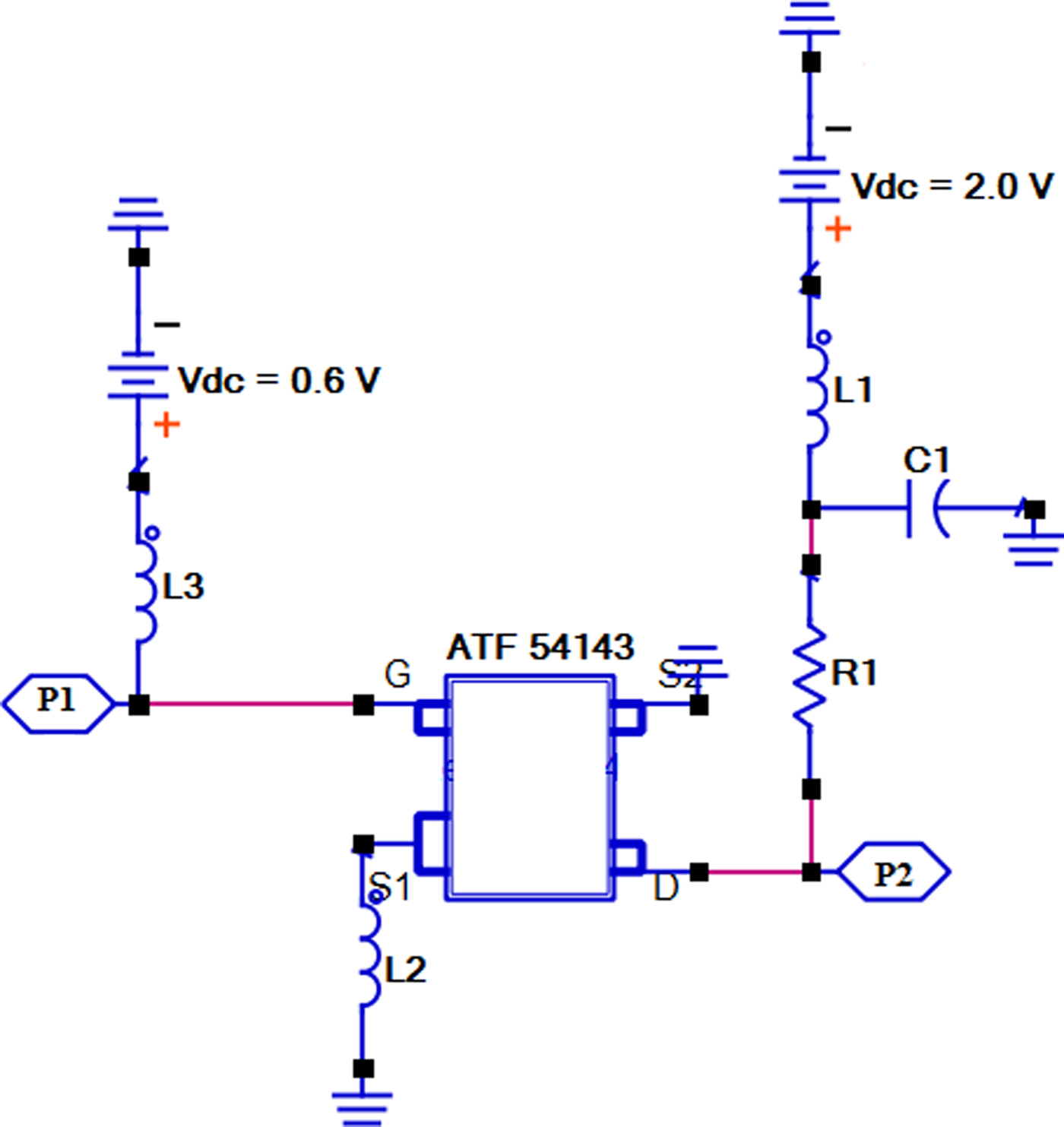
Fig. 6. Schematic of the proposed amplifier.
2) IMPEDANCE MATCHING
To accomplish maximum power transfer, it requires complex conjugate matching. In general, adjusting the source impedance or the load impedance is called impedance matching.
Input matching
One of the approaches to achieve impedance matching is filter design. In our work, to achieve multi-band impedance matching at the input port, we employed frequency transformation method [Reference Roy24]. The basic LC network used for multi-band matching network is shown in Fig. 7.
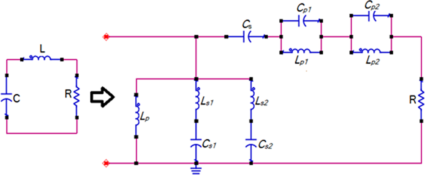
Fig. 7. Input matching circuit.
One appropriate transformation for this case is given in equation (6).
 $$S =\, \displaystyle{{g_0} \over s} + \displaystyle{{g_1 s} \over {(s^2 + q_1 )}} + \displaystyle{{g_2 s} \over {(s^2 + q_2 )}}.$$
The impedance of L (=R1) is transformed as in equation (7).
 $$SL_1 = {\rm \;} \displaystyle{{(g_0 R_1 )} \over s} + \displaystyle{{(g_1 R_1 )s} \over {(s^2 + q_1 )}} + \displaystyle{{(g_2 R_1 )s} \over {(s^2 + q_2 )}}.$$
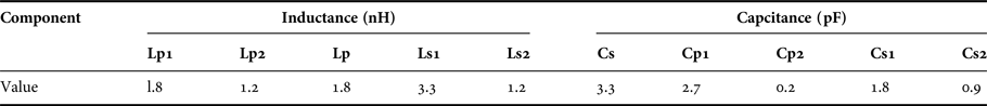
The right-hand side of the equation (7) signifies a series connection of the capacitance, C s = 1/g0R1 and parallel combination of the LC, L p1 = g 1 R 1/q 1, L p2 = g 2 R 1/q 2, C p1 = 1/g 1 R 1, and C p2 = 1/g 2 R 1. To find the values of unknown variables, we continued solving by substituting S = j1 and s = j ω in equation (6) with the roots ω 5, −ω 4, ω 3, −ω 2, and ω 1.
 $$(\omega + \omega _1 )(\omega - \omega _2 )(\omega + \omega _3 )(\omega - \omega _4 )(\omega + \omega _5 ) = 0,$$
 $$\eqalign{& \omega ^5 + \omega ^4 (g_0 + g_1 + g_2 ) - \omega ^3 (q_1 + q_2 ) \cr &\quad - \omega ^2 (g_0 q_1 + g_0 q_2 + g_1 q_2 - g_2 q_1 ) + \omega (q_1 q_2 ){\rm } + g_0 q_1 q_2 = 0.} $$
By equating both equations (8) and (9) we get,
 $$g_0 + g_1 + g_2 = \omega _1 - \omega _2 - \omega _3 + \omega _4 - \omega _5, $$
 $$\eqalign{q_1 + q_2 & = \omega _1 \omega _2 + \omega _2 \omega _5 - \omega _1 \omega _5 - \omega _2 \omega _4 + \omega _1 \omega _4 + \omega _4 \omega _5 \cr & \quad + \omega _2 \omega _3 - \omega _1 \omega _3 - \omega _3 \omega _5 + \omega _3 \omega _4,} $$
 $$\eqalign{g_0 (q_1 + q_2 ) + g_1 q_2 - g_2 q_1 & = \omega _1 \omega _2 \omega _5 - \omega _1 \omega _2 \omega _4 - \omega _2 \omega _4 \omega _5 \cr & \quad + \omega _1 \omega _4 \omega _5 + \omega _1 \omega _2 \omega _3 + \omega _2 \omega _2 \omega _5 \cr & \quad - \omega _1 \omega _3 \omega _5 - \omega _2 \omega _3 \omega _4 + \omega _1 \omega _3 \omega _4 \cr & \quad + \omega _3 \omega _4 \omega _5,} $$
 $$\eqalign{q_1 q_2 & = - \omega _1 \omega _2 \omega _3 \omega _5 + \omega _1 \omega _2 \omega _4 \omega _5 + \omega _1 \omega _2 \omega _3 \omega _4 \cr & \quad + \omega _2 \omega _3 \omega _4 \omega _5 - \omega _1 \omega _3 \omega _4 \omega _5,} $$
 $$g_0 q_1 q_{2} = \omega _1 \omega _2 \omega _3 \omega _4 \omega _5. $$
By solving the above equations, we obtained g 0, g 1, g 2, q 1, and q 2 as 13.69 × 10⁹, 4.70 × 10⁹, 10.49 × 10⁹, 1.1038 × 10²⁰, and 5.375 × 10²⁰, respectively. By substituting g 0, g 1, g 2, q 1, and q 2 values, we calculated the capacitance and inductance values. Here, the L and C values collectively decide the desired penta band. Table 1 lists the optimized values of inductance (nH) and capacitance (pF) used. The insertion loss provided by the designed input matching circuit was checked with S parameter simulation, is plotted in Fig. 8. The insertion loss is found to be below 5 dB at all desired frequency bands making it suitable for furtherance of LNA design.

Fig. 8. Insertion loss profile of input matching circuit.
Table 1. Input matching circuit components list.
Output matching
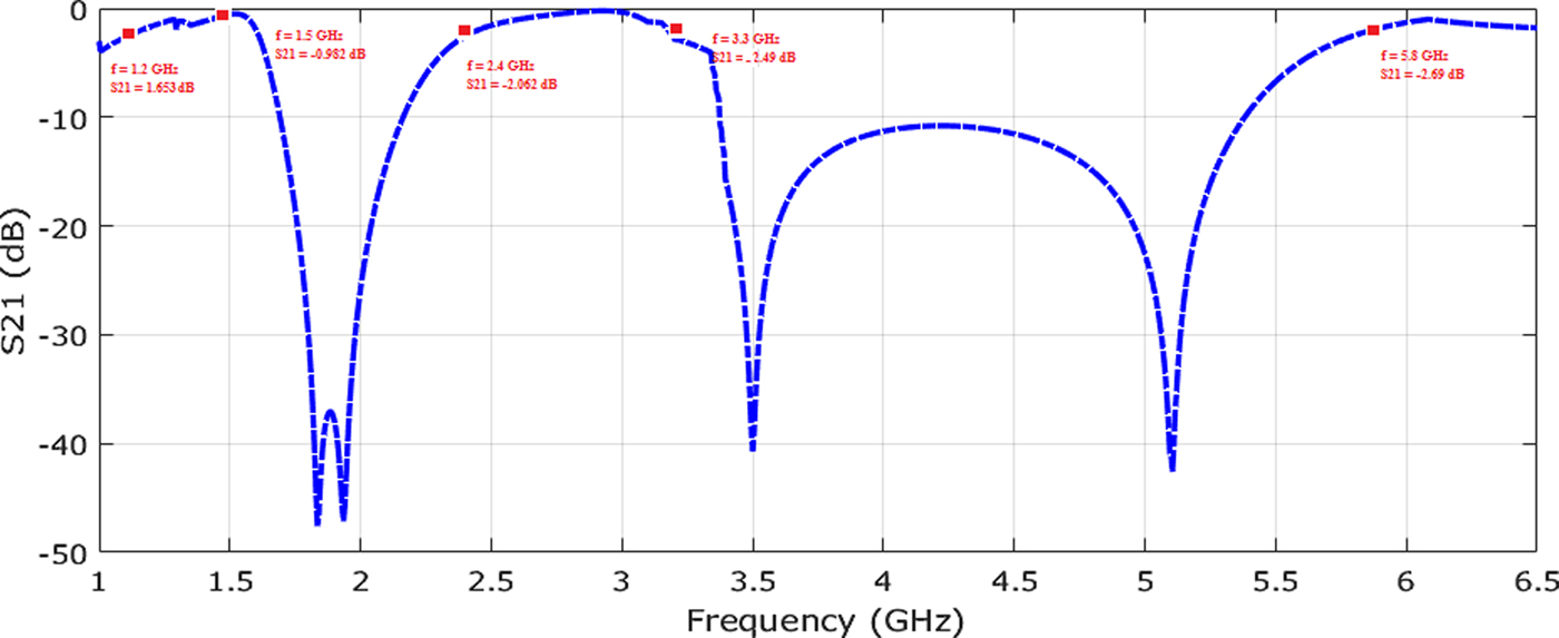
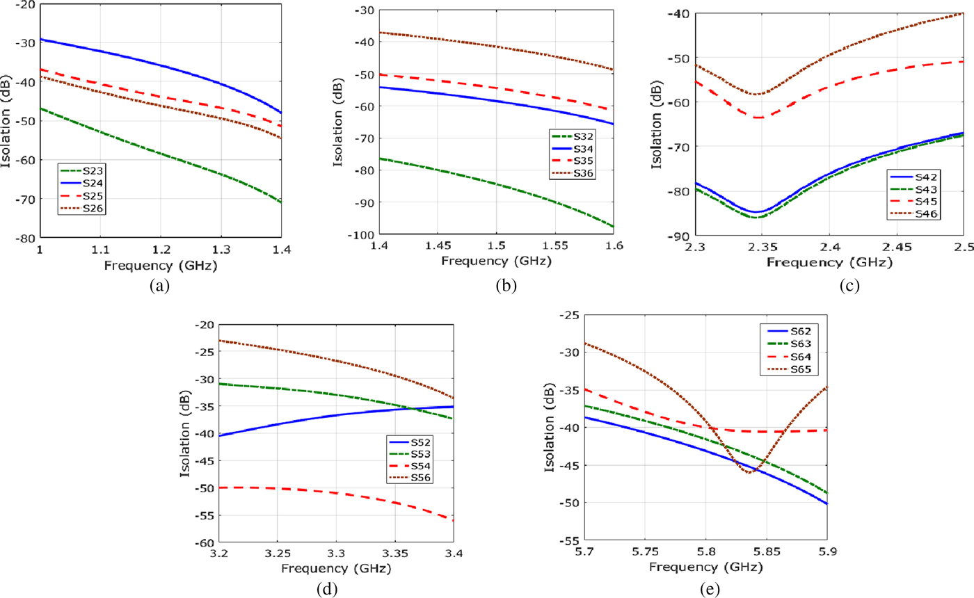
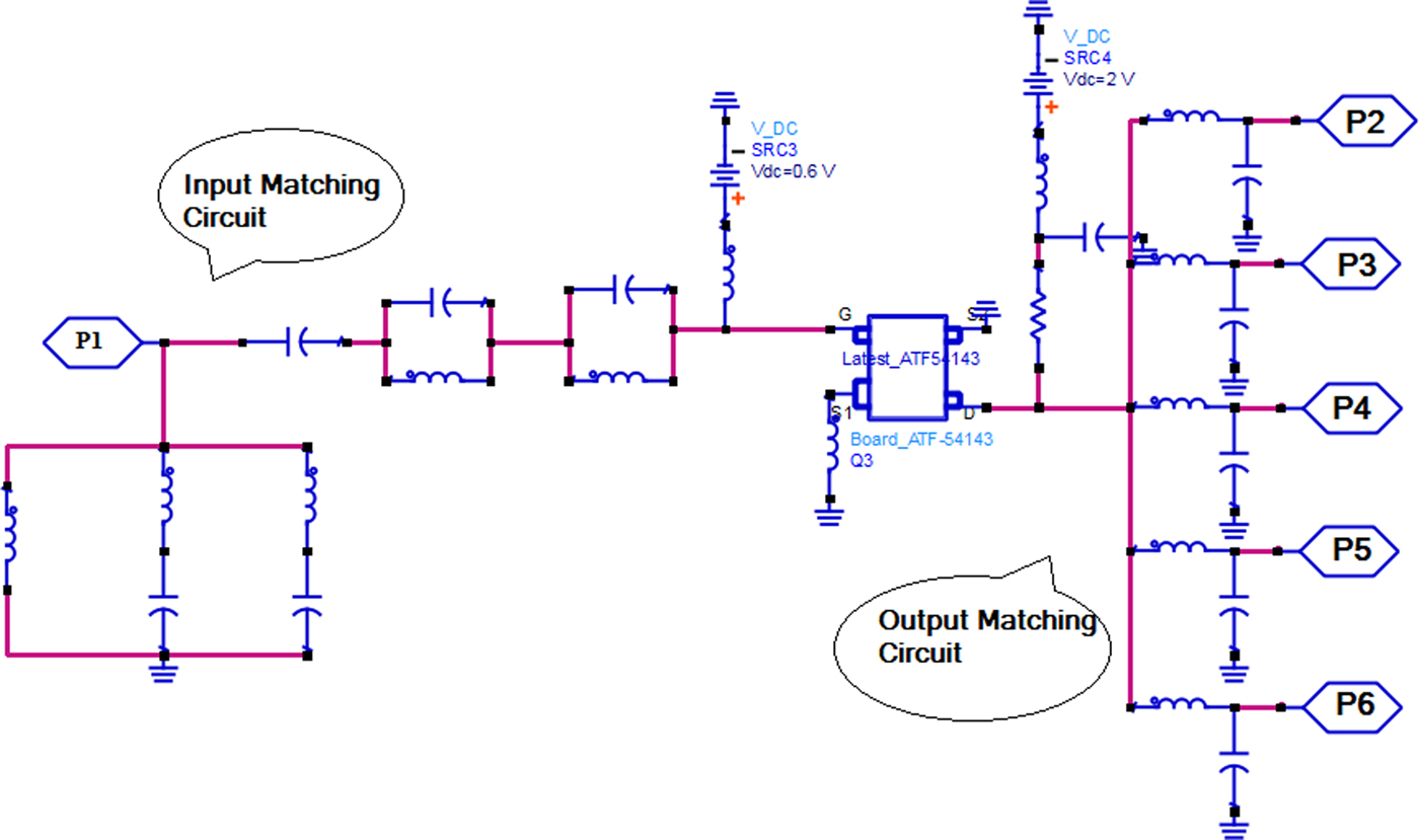
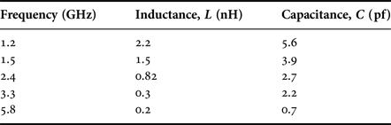
In general, conjugate matching is used for narrow band LNA design to achieve maximize the gain. With additional third-order intercept point (IP3) constraint imposed on the LNA, the trade-off between IP3 and gain need to be considered. The load−pull techniques [Reference Tuijtelaars25] are used to determine an output match that provides an appropriate trade−off between gain, OIP3, and P1 dB in the same way as for a power amplifier. In order to achieve better linearity with good gain, utilized a load-pull technique in our proposed design. The load-pulling method sweeps impedance of the whole Smith chart and plots contours of constant gain and IP3 numbers. It allows adjusting independently the resistive and reactive components. We found the optimum impedance of the circuit at each desired frequency individually, the point where the gain does not degrade as much and the IP3 is still respectable. The optimum impedance attained at 1.2, 1.5, 2.4, 3.3, and 5.8 GHz are 25.3514 − j13.895, 24.457–10.361, 30.705 − j11.895, 36.384 − j9.163 and 16.512 + j163, respectively. Using ADS's smit chart tool, matched the obtained optimum impedance to 50 Ω impedance with respect to corresponding frequencies. Then performed optimization to get desired output and isolation among each other frequencies and validated the isolation between each frequencies with S parameter analysis (Isolation loss). Figure 9 shows the isolation loss among each output ports and isolation lass observed to be better than 25 dB corresponds to each output ports. To achieve simultaneous reception of multi-band signal, with the obtained optimum impedance, distinct impedance matching circuit at all desired frequency is designed with simple LC circuit. Figure 10 shows the LC Output matching network and Table 2 gives the inductance and capacitance value used for the design to match with 50 Ω at all the desired frequencies. Figure 11 shows the circuit diagram of the proposed LNA with matching circuits. At higher frequencies while doing prototype, there will be a transmission line effect. Hence, we optimized and simulated the design considering transmission lines with layout design utilizing ADS's co-simulation tool. The layout design of proposed LNA is shown in Figure 12.

Fig. 9. Isolation between output ports. (a) at port 2, (b) at port 3, (c) at port 4, (d) at port 5, and (e) at port 6
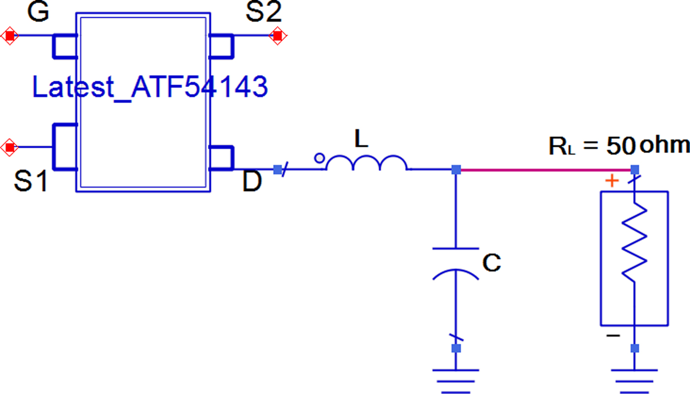
Fig. 10. Output matching circuit.

Fig. 11. Schematic of concurrent penta-band LNA with the biasing circuit.

Fig. 12. Layout of concurrent penta-band LNA with the biasing circuit.
Table 2. Output matching circuit component list.
B) Results and discussion
The ATF-54143 from Avago Technologies is picked as an active component for the proposed LNA design. It is operated in enhancement-mode GaAs pHEMT technology. The other passive components, capacitors, and inductors are with chip packing from AVX, Kyocera group of company and TOKO, INC. The entire LNA is on a FR4 board with a relative dielectric constant of 4.4 and thickness of 1.57 mm and draws 60 mA from the 2 V supply. Figure 13 shows the prototype of the penta-band LNA.

Fig. 13. Prototype of penta-band LNA.
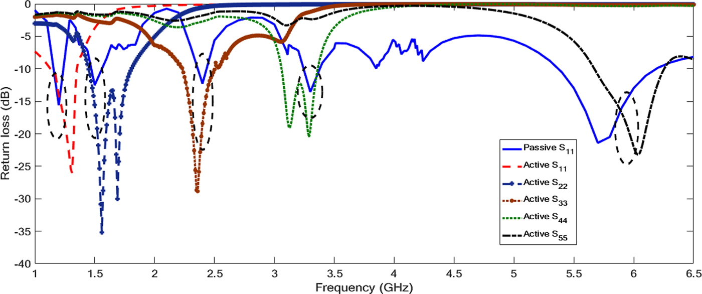
In LNA design the impedance matching, gain, NF and linearity are the essential parameters. Hence, we mainly motivated on analyzing the mentioned characteristics. Figure 14 shows the measured return loss at input and output ports. As could understand, both input and output return loss are better than 12 dB across all desired five bands and operates simultaneously at 1.2,1.5 GHz (navigation), 2.4 and 3.3 GHz (wireless communication), and 5.8 GHz (DSRC). It shows an efficacious design of our input and output matching circuit.
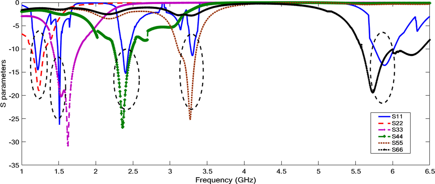
Fig. 14. Input and output return loss of penta-band LNA.
The measured gain of the penta-band LNA with respect to each output port is plotted in Fig. 15. At all, working frequencies achieved gain >10 dB. It shows, a flat gain is obtained over the all desired working bands except at 1.2 GHz. The simulated NF of the penta-band LNA with respect to each output port is plotted in Fig. 16. NF <2 dB is observed at all desired frequencies.
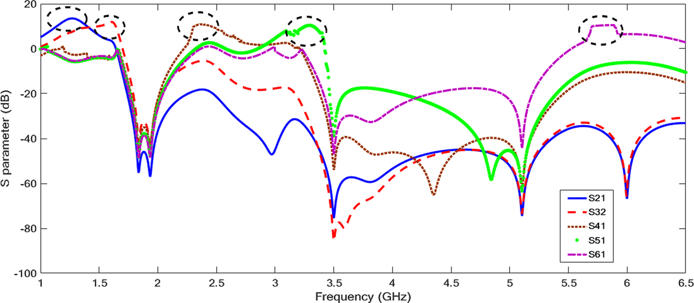
Fig. 15. The Gain of the proposed LNA at desired frequencies.
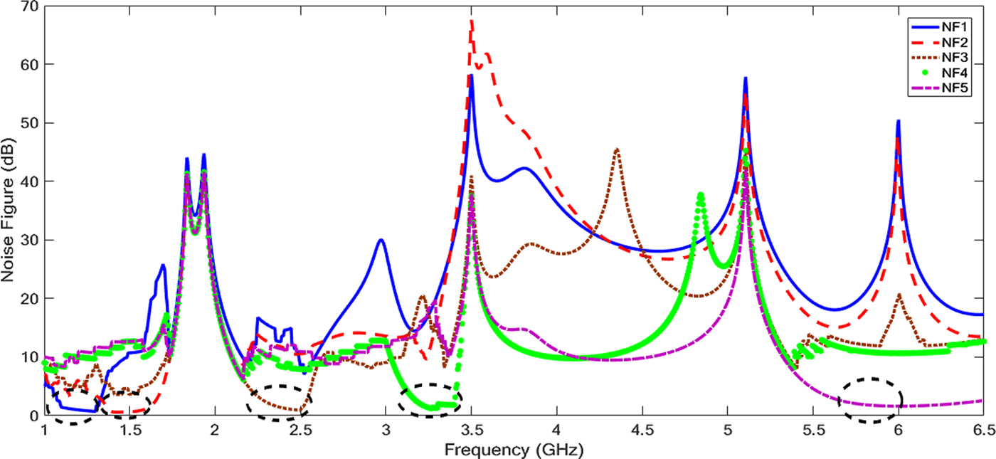
Fig. 16. The NF of the proposed antenna at desired frequencies.
Gain compression and IP3 are significant nonlinear characteristics of RF circuits and help in proving circuit's linearity and dynamic range. Intermodulation distortion (IMD) behavior is examined using a two-tone harmonic balance test with 1 MHz spacing. Figure 17 shows the IMD analysis of our LNA. We obtained −1.061, −1.063, 0.0428, 2.684, and 5.403 dBm at working frequencies 1.2, 1.5, 2.4, 3.3, and 5.8 GHz, respectively. This verifies the linear characteristics of the LNA. Table 3 encapsulates the performance of the proposed penta-band LNA.
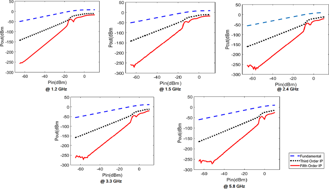
Fig. 17. IMD behavior analysis of penta-band LNA.
Table 3. The performance of Penta-band LNA.
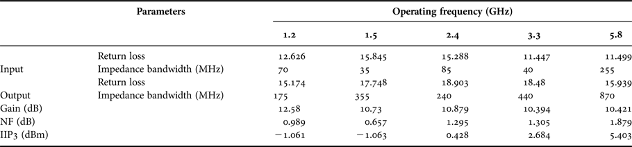
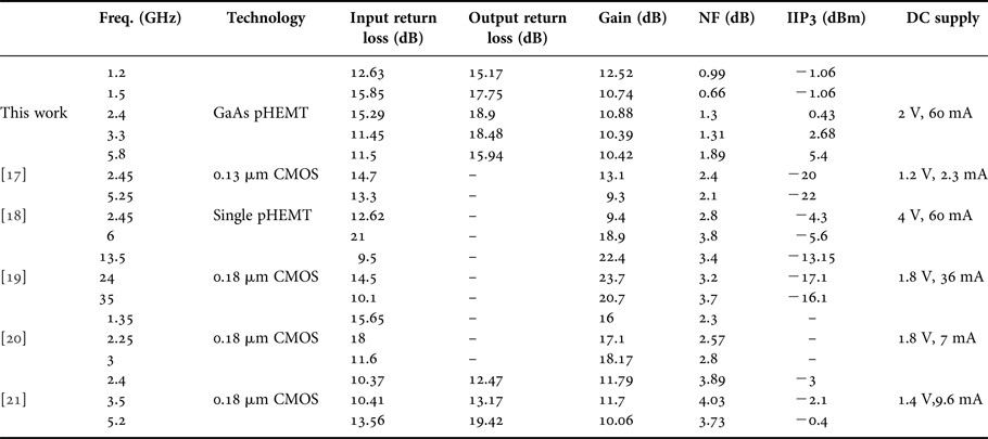
Table 4 summarizes the performance of the proposed concurrent penta-band LNA and those of published concurrent penta-band LNAs. As can be seen, this work point up lowest NF and good linearity performances in all operating bands. Though the gain of proposed LNA is slightly lesser than other LNAs, it has an acceptable gain greater than 10 dB, better linearity, and better input/output return loss lesser than 15 dB in all bands.
Table 4. Performance summary of proposed concurrent penta-band LNA and existing concurrent Penta-band LNAs.
IV. DESIGN AND ANALYSIS OF INTEGRATED ACTIVE ANTENNA (IAA)
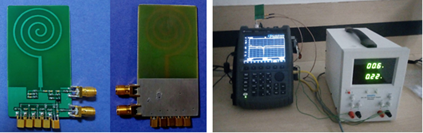
Two key components in the design of IAA are omnidirectional planar spiral microstrip antenna and LNA. Each of them was designed individually before being integrated as one to form an active integrated antenna as discussed earlier. Figure 18 shows the circuit schematic of IAA. The input matching circuit optimization is done using Keysight's Advanced Design Systems to ensure conjugate matching of reflection coefficient of the proposed antenna and LNA thus providing larger impedance bandwidth and compactness at the band of interest. Figure 19 shows the prototype and measurement set up of IAA. Here, the receiver ports are connected with Molex MMCX (ST JACK PCB) connectors. For measurement purpose MMCX PLUG to SMA PLUG adapter has been used. The Keysight's N9926A Vector Network Analyzer is used to validate the antenna performances and regulated power supply is used to supply bias voltage.

Fig. 18. Schematic of proposed IAA.

Fig. 19. Photograph of proposed IAA and measurement set up.
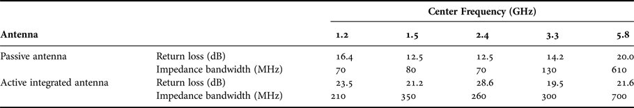
The antenna resonates at five desired frequency bands, 1.2, 1.5, 2.4, 3.3, and 5.8 GHz. The return loss comparison of passive antenna and IAA is shown in Fig. 20. We infer that with IAA it is possible to achieve better impedance matching, which reflects as better return loss. Table 5 gives the performance comparison of passive and integrated active antenna. It evidences proposed active integrated antenna has an improved bandwidth and better return compared with passive antenna.

Fig. 20. Comparison of passive antenna and IAA return loss.
Table 5. Performance comparison of passive antenna and IAA.
V. CONCLUSIONS
This paper describes the design and analysis of the penta-band LNA with active antenna, which operates concurrently at all desired frequency bands of 1.2, 1.5, 2.4, 3.3, and 5.8 GHz. The distinct LNA design helps to achieve low NF (<2 dB) with good linearity. With the proposed IAA return loss more than 19 dB and impedance bandwidth more than 200 MHz was achieved at all bands. The result proves that the proposed integrated antenna design helps to achieve better return loss and improved impedance bandwidth compared with passive antenna module. This integrated antenna is simple in its design and could easily be redesigned to meet the requirements of rapidly growing vehicular wireless applications.
ACKNOWLEDGEMENTS
The authors are grateful to the service supported by the Green Pearl Electronics and Amphenol Omni-connect India Private Limited, Chennai, India in circuit assembling and measurements.
 Ramya Vijay received her M. Tech. Degree in Information Communications Technology from Visvesvaraya Technological University, India in 2010 and is currently pursuing her Ph.D. degree in Telecommunication engineering, SRM University. Her main research interests are design and analysis of antenna and propagation for vehicular communication.
 Thipparaju Rama Rao is a Professor of Telecommunication Engineering at SRM University, India, and has long-standing research experience on Radio Communications. Earlier, he worked at Aalborg University, Denmark as a Research Professor, at Universidad Carlos III de Madrid, Spain, and at the University of Sydney, Australia, as a Visiting Professor. Professor Rama Rao has been receiving significant funding from the Government of India, to develop high performance millimeter-wave antennas at 60 GHz and associated transceiver circuit for gigabit wireless applications. He is also working on inter-satellite radio link investigations at millimeter-waves with funding from the ISRO and developing wearable antennas for wearable device applications for DRDO. He is a member of IEEE, WWRF, IET, ACM, and IETE. So far, he has supervised ten Ph.D. students and authored 50+ papers in reputed journals and 90+ in various conferences. His research interests include Antennas & Its Applications, Broadband & Mobile Cellular Telecommunications.
 Dr. Revathi Venkataraman is currently working as Professor in Department of Computer Science Engineering, SRM University, India. She received her Ph.D. from SRM University, Tamil Nadu, India. She has authored more than 30+ papers in reputed journals/transactions and international/national conferences and her research interests include Wireless Sensor Networks, Trust Computing, Security enhancements and privacy considerations for IoT. She has received funding from Defence Research Development Organization and has developed many use cases and security modules for wireless protocols.
 Dr. Murugiah Sivashanmugham Vasanthi graduated in Electronics from Bangalore University, India in 1994 and completed her post graduation in Communication Systems from Anna University, Chennai, India in 2004. She received her Ph.D. degree on the topic “Investigations on Radio Frequency Transceiver issues for Wireless Sensor Communications” from SRM University, India. She is currently working as Assistant Professor in the Department of Telecommunication Engineering, Faculty of Engineering & Technology, SRM University, India. Her major research interests include design of wireless RF transmitters and receivers and energy efficient transceiver design techniques. Dr. M. S. Vasanthi is a member of the IEEE Communication Society, Life member of Indian Society for Technical Education (ISTE), Institute of Electronics and Telecommunication Engineers (IETE) and member of the Indian Science Congress Association (ISCA).