I. INTRODUCTION
As device manufacturers try and maintain Moore's law, the physical limits of usual techniques and materials in electronics become more and more difficult to circumvent. Great hopes lie in the use of new materials, such as carbon nanotubes (CNTs) or graphene. They present a high conductivity, resistance to electromigration, fast time response. However, efforts have mainly been focused on realizing CNT components such as field-effect transistors (FETs) or sensors often overlooking their connection to more conventional electronics. Those devices are intrinsically small and high-impedance and metal-CNT contacts are still to date high-resistance and difficult to reproduce. A wireless connection to these components would be highly beneficial by remediating to problems of high-precision contacting and impedance matching especially if the same CNTs can be used to accomplish the component function and to radiate.
When applied to the case of antennas, CNTs could also help miniaturization from a different perspective. In fact, the ever increasing needs in connectivity and high data rate for portable devices equate with the integration of multiple antennas with a non-negligible footprint. Antennas need to be resonant to offer good radiation performance, which sets a minimum length of about a quarter wavelength at nominal frequency – centimeters for Wi-Fi. However, CNTs present a high kinetic inductance [Reference Burke, Li and Yu1] that results on slow-wave propagation along their axis and thus a resonant antenna size reduction of up to 50 [Reference Burke, Li and Yu1, Reference Hanson2].
II. CNT MODELLING
A) Models
We rely on two complementary approaches to model CNTs integrated in electronic components. Firstly, a circuit approach, derived from [Reference Burke, Li and Yu1, Reference Burke3, Reference Burke4], secondly, an electromagnetic (EM) approach [Reference Franck, Baillargeat and Tay5] based on [Reference Slepyan, Maksimenko, Lakhtakia, Yevtushenko and Gusakov6]. These models are inherently limited to the case of metallic single-wall carbon nanotubes (m-SWCNTs) of limited diameter (a max = 6.8 nm) studied at frequencies up to 30 THz – below interband transition regime [Reference Slepyan, Maksimenko, Lakhtakia, Yevtushenko and Gusakov6, Reference Shuba, Slepyan, Maksimenko, Thomsen and Lakhtakia7]. In these conditions, semiconducting CNTs contribution can be neglected as their conductivity is 2 to several orders of magnitude smaller than that of the metallic ones [Reference Slepyan, Maksimenko, Lakhtakia, Yevtushenko and Gusakov6] and both species are typically present in similar quantities in unsorted CNTs. There exist appropriate models [Reference Shuba, Slepyan, Maksimenko, Thomsen and Lakhtakia7, Reference Naeemi and Meindl8] to deal with the cases that exceed these limits and they can be implemented following the same approaches. However, the current description is focused on the most interesting case for antennas. Indeed, kinetic inductance decreases with increasing CNT diameter and number of shells [Reference Naeemi and Meindl8] thus lessening the shortening effect we seek by using CNTs in antennas.
The circuit model relies on a transmission line approach where the traditional electrostatic capacitance, magnetic inductance and resistance are completed with a kinetic inductance – predominant in CNTs – and a quantum capacitance [Reference Burke3, Reference Burke4]. Once derived, a circuit model allows quick analysis of simple structures and we use it to make physical sense of our results on monopole and dipole antennas. Nonetheless, in the case of most realistic antennas or to study radiation and feed structures, a three-dimensional (3D) EM simulation is necessary. The available EM model for CNTs was however incompatible with finite-element analysis of more than a few CNTs. It describes each CNT as a shell with given surface conductivity [Reference Hanson2, Reference Slepyan, Maksimenko, Lakhtakia, Yevtushenko and Gusakov6], which makes it extremely difficult to mesh and solve because of the many scales involved. CNT diameters are in the 0.1–6.8 nm range, CNT lengths and microelectronic components in the 0.1–1000 µm range and there can be anywhere between a single CNT and billions of CNTs.
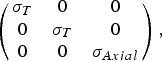
To address this matter we have developed a mesoscopic model based on an effective medium approach and the model in [Reference Slepyan, Maksimenko, Lakhtakia, Yevtushenko and Gusakov6]. SWCNTs are modeled using a material with anisotropic complex EM properties as originally described in [Reference Franck, Baillargeat and Tay5]. We use published values for the phenomenological constants. The complex conductivity of an array of CNTs aligned along the z-axis in Cartesian coordinates can be written:
 $$\left({\matrix{ {\sigma _T } & 0 & 0 \cr 0 & {\sigma _T } & 0 \cr 0 & 0 & {\sigma _{Axial} } \cr } } \right)\comma \;$$
where σ T is the transverse conductivity and σ Axial the axial conductivity. In the cases studied here the aligned CNTs are excited in common mode, separated by a dielectric, and their lateral spacing is large enough to prevent CNT-to-CNT transverse conductivity as defined in [Reference Franck, Baillargeat and Tay5]. Hence, σ T = 0 and, for a cross-sectional CNT density D NT, the complex axial conductivity is:
 $$\sigma _{Axial}=\sigma _{lin\comma 0} {\rm \; }D_{NT} {\rm \; }\zeta \lpar u\rpar \comma \;$$
where
 $$\sigma _{lin\comma 0}=\displaystyle{{8e^2 v_F } \over {h\nu }}=\displaystyle{{24e^2 b\pi } \over {h^2 }}\displaystyle{{\gamma _0 } \over \nu }=A\gamma _0 \tau$$
is the DC linear conductivity over a single SWCNT. It is linearly dependent on the phenomenological values γ0 and τ = ν −1, the overlap integral in the tight-binding description and the plasmon lifetime in the SWCNTs used, and taken to be 3 eV and 3 ps respectively for the numerical applications in this paper. The complex frequency dispersion profile and the normalized frequency are respectively:
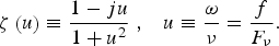 $${\rm \zeta }\left(u \right)\equiv \displaystyle{{1 - ju} \over {1+u^2 }}\; \comma \; \; \; u \equiv \displaystyle{\omega \over \nu }=\displaystyle{f \over {F_\nu }}.$$
Note that the conductivity is predominantly complex only for f > F ν = 1/2πτ = 53 GHz for the chosen value of τ which is for excellent CNT quality. The quality of the CNTs used is thus a prime concern to ensure the feasibility of resonant antennas.
B) Implementation
The circuit model can be used to derive analytical formulas, which allow a better understanding of a structure. In the case of monopole and dipole structures we have derived and implemented these formulas in an Excel sheet to allow direct comparison with the EM results, further study of the trade-offs we will outline in the following sections and performance prediction before additional EM simulation [Reference Franck, Baillargeat and Tay9]. The circuit model can also be implemented in Agilent's ADS [Reference Brun10] for more complicated structures.
The EM model is implemented in HFSS (Ansys) and EMXD (developed by Michel Aubourg at XLIM) – two frequency-domain 3D EM solvers both based on the finite-elements method. The implementation in EMXD allowed the validation of the model thanks to a point-by-point definition of the mesh in the open-source mesh generator GMSH and to non-ambiguous definition of complex conductivity in EMXD. HFSS, as a commercial distribution, is more widely available and a more versatile simulation suite.
It is then possible to select CNTs among other conventional materials while keeping control over the model parameters. This modeling approach has been validated by direct comparison with published theoretical and experimental results [Reference Hanson2, Reference Yang11]. Its equivalence to the model it is derived from (individual hollow tubes) has been demonstrated (cf. Fig. 1) while considerably cutting the simulation time and required memory. It is well suited for the study of mesoscopic configurations like those presented in the following section where the previous method would fail.

Fig. 1. Schematic illustration of the effective medium model and radial electric field distribution in a CNT monopole showing the equivalence of the hollow tube model (left) and the effective medium (right).
III. STUDY OF SIMPLE DESIGNS
As a first step to understand the trade-offs involved in designing CNT-based electrically-short resonant antennas, a parametric study on m-SWCNT monopoles was undertaken [Reference Franck, Baillargeat and Tay9, Reference Franck, Baillargeat and Tay12]. Indeed, if a single SWCNT is expected to slow waves down by a factor of 50 [Reference Burke, Li and Yu1, Reference Hanson2], it should also be outlined that it presents a much too high input impedance to be connected to usual 50-ohm electronics and to radiate effectively. A SWCNT has typical resistivity of a few kΩ/μm multiplied by a length of tens to hundreds of micrometers in our application with an additional contact resistance of a few kΩ [Reference Burke3, Reference Buttiker and Christen13, Reference Lan, Srisungsitthisunti, Amama, Fisher, Xu and Reifenberger14] if ohmically contacted to a metal. It is thus necessary to use multiple CNTs in parallel to reduce and tune the input impedance of this antenna.
The chosen structure is a simple quarter-wavelength monopole. It consists of a vertical metal rod over a ground plane. In our case the metal rod is replaced by a bundle of CNTs. Then we vary the number of CNTs, N CNT and their length, L CNT. It appears that simply adding CNTs in parallel does not work. The resonance frequency scales inversely with L CNT but it shifts higher when CNTs are added in parallel thus degrading the size reduction we are after [Reference Franck15].
Indeed putting N CNT CNTs in parallel results in dividing the overall impedance and thus the kinetic inductance by N CNT: Z total = Z CNT/N CNT = R CNT/N CNT + jωL k/N CNT. Neglecting the magnetic inductance and resistance, the propagation velocity along the CNTs can be written:
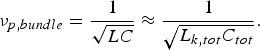 $$\nu_{p{\rm\comma }bundle}=\displaystyle{1 \over {\sqrt {LC} }} \approx \displaystyle{1 \over {\sqrt {L_{k\comma tot} C_{tot} } }}.$$
Moreover, because the total capacitance has relatively small variations with N CNT, we obtain:
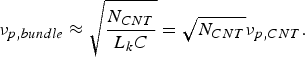 $$\nu_{p\comma bundle} \approx \sqrt {\displaystyle{{N_{CNT} } \over {L_k C}}}=\sqrt {N_{CNT} } \nu_{p\comma CNT}.$$
Hence, as a first approximation, the impedance is inversely proportional to N CNT and proportional to L CNT, whereas the resonance frequency is proportional to  $\sqrt {N_{CNT} } $ and inversely proportional to L CNT. A trade-off thus needs to be found between size reduction, operating frequency and input impedance (cf. Fig. 2). For an antenna with good size reduction <100–1000 CNTs should be used. For it to be well-matched to 50 Ω, short CNTs thus need to be used and this leads to working at extremely high frequencies: 200 GHz and higher. Lower frequencies and good size reduction are possible at higher impedance.
Fig. 2. Illustration of the trade-offs in terms of size reduction (left), impedance match (right, the usual return loss in dB is replaced by a linear fraction of accepted power better suited to comparing slightly mismatched antennas) and resonance frequency (the two curves highlighted through the case when S11=−5 dB)
The next section describes experimental considerations and additional parametric studies led toward realizing a real electrically short resonant antenna from CNTs. The trade-offs explained here are maintained in these planar dipole structures.
IV. EXPERIMENTALLY FEASIBLE DESIGNS
The experimental realization of these antennas is a complex task. The study presented in the previous section demonstrates the need for long high-quality SWCNTs in specific quantities which takes us to the limits of current CNT fabrication techniques. There are a few types of CNT fabrication methods, each with their particular advantages and restrictions. To observe experimentally a size reduction on a resonant antenna, these need to be considered along with simple antenna designs.
We will study monopole and dipole antennas where the axial propagation of electrons corresponds best to CNTs. The simplicity of the structure also ensures correct interpretation of the results.
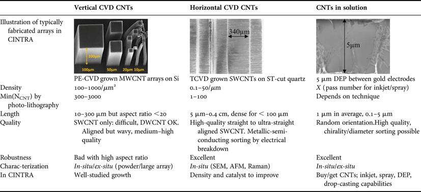
As base material, three types of CNTs can be used. Dense vertical CNT arrays can be obtained by thermal (T) or plasma-enhanced (PE) chemical vapor deposition (CVD); with typical densities of 1010–1011/cm2. Substrate-lattice-aligned horizontal CNTs can also be obtained by CVD on specific substrates such as quartz [Reference Kocabas, Shim and Rogers16] then, optionally, transferred, even at wafer scale [Reference Patil17]; reported densities range up to 50/μm [Reference Ding, Yuan and Liu18] but are usually from 0.1 to 10/μm – we have achieved 1/μm so far. Solution-processed CNTs can be deposited by a variety of methods rather than in-situ grown. Additionally photolithography is preferable for its simplicity and scalability for catalyst and electrode patterning and imposes a lower resolution limit of about 2 µm. These methods are compared in Table 1.
Table 1. Different CNT types for the fabrication of an electrically short resonant antenna.
We conclude that only CVD-grown CNTs provide us with the necessary lengths for our application. Tunneling junction transmission through multiple solution-deposited CNTs would dampen the wave. Vertical CNTs allow the fabrication of long CNTs but, for low N CNT, involve high-aspect-ratio standing structures difficult to realize. This fabrication process being well mastered in CINTRA monopole designs relying on it are under study [Reference Brun, Franck, Coquet, Baillargeat and Tay19]. The lattice-aligned horizontal CNTs seem to be the best logical choice with high-quality ultra-straight SWCNTs easier to connect and characterize.
The proposed design thus relies on CNTs grown by TCVD on an ST-cut quartz wafer. The first fabrication step is the patterning of metal catalyst lines. Usual lithography techniques can be used in conjunction with ebeam evaporation or spin-coating of a solution of metallic ions [Reference Zhou, Rutherglen and Burke20]. We adopted the technique described in [Reference Li21, Reference Cao22] which consists in scratching the substrate with a metallic object. CNTs are then obtained by CVD growth, before optional O2 plasma etch of unwanted CNTs and eventually the patterning and evaporation of metal electrodes.
The proposed antenna is illustrated in Fig. 3 while the fabrication process is demonstrated by the fabrication of a CNT characterization structure: a coplanar waveguide (CPW) cut by a gap bridged by a few CNTs (Fig. 4). A CPW feed of the proposed antenna is under study. A full parametric study of the antenna has been led [Reference Franck, Baillargeat and Tay23, Reference Franck, Baillargeat and Tay24]. As expected, trends similar to those of the ideal monopole arise (cf. Fig. 5): the size reduction is only dependent over the N CNT used: K red ≈ 50/√N CNT, while f ≈ (1600/L CNT)*√N CNT and Z in ≈ (400*L CNT)/N CNT in (μm, GHz, Ω).
Fig. 3. CNT dipole on quartz substrate that would be realized by lattice-aligned CVD growth then O2 plasma etching.
Fig. 4. Demonstration of the fabrication process by the fabrication of Au/Ti CPW gap electrodes over CVD grown CNTs.
Fig. 5. Simulated characteristics of 50-Ω-fed planar SWCNT-based dipoles as a function of (N CNT, L CNT). (a) Resonance frequency and input impedance. (b) Size reduction and return loss. Dipole lengths are 40 (▴), 80 (•), 160 (X), 320 (♦), and 640 (■) μm with 4 µm gap.
Here the study is limited to VNA measurable frequencies – up to 300 GHz. When limited to these frequencies our abacus shows that the input impedance necessarily exceeds 200 Ω for configurations of less than 256 CNTs, which coincides with a reduction factor K red ≈ 4. Hence to operate with 50-Ω electronics at technologically relevant frequencies, one should not expect to reduce the size of their CNT resonant antenna more than four times with respect with the metal one.
Another, maybe more interesting, application of these antennas is an asymmetric wireless link acting like an impedance transformer between high-impedance nanocomponents directly connected to/incorporating an impedance-matched CNT antenna and usual microelectronics connected to a classical directive antenna [Reference Franck, Baillargeat and Tay24].
V. CONCLUSION
We have described convenient simulation tools for the study of CNT-based electrically short resonant antennas. We have outlined trends and design rules as well as fabrication techniques and initial designs for these antennas. Finally, we have discussed possible applications of these antennas. They seem to be an interesting solution for the developing field of RF above 100 GHz. They can also be used to wirelessly connect high-impedance nanocomponents to conventional electronics. Design and fabrication in this direction are ongoing.
ACKNOWLEDGEMENT
This research is co-funded by the French DGA and CNRS.
 Pierre Franck received the Diplôme d'Ingénieur (Master of Engineering) from Institut d'Optique Graduate School, ParisTech, Palaiseau, France in 2010 and the MSc in Applied Optics and Photonics from Imperial College London, London, United Kingdom in 2010. He worked on femto-second lasers at CEA Saclay and human-computer interaction at Imperial College. He is currently working towards the Ph.D. degree at the CNRS-International-NTU-THALES-Research-Alliance (CINTRA) in Singapore and XLIM in Limoges, France. His current interests are in design, modeling, fabrication and characterization of carbon-nanotube-based electronic and optoelectronic components with a focus on antennas.
Dominique Baillargeat received the Ph.D. degree in 1995 from the University of Limoges, France. From 1995 to 2009, he was associate professor then professor at XLIM Research Institute, University of Limoges. From 2009 to 2013, he was director of the CNRS- International-NTU-THALES-Research-Alliance (CINTRA) in Singapore. From 2013, he is director at XLIM in Limoges, France.
His research work is mainly in the following areas: (1) EM simulation and hybrid modeling coupling electromagnetic, circuits and thermal analysis, synthesis and electromagnetic optimization techniques. (2) Design and (nano)packaging of millimeter wave and optoelectronics modules, based on innovative (nano)technologies/(nano)materials. He authored or co-authored more than 150 technical papers in journals or conferences.
Prof. Baillargeat acts as expert for the French Research Agency (ANR) and French Ministry of Research . He acts as reviewer for IEEE MTT, IEEE MWCL and EuMW.
 Tay Beng Kang received his degree in engineering (1985) and M.Sc. (electrical engineering, 1989) from the National University of Singapore and his Ph.D. from the Nanyang Technological University of Singapore in 1999. He became a full university professor in 2006 and is currently the Program Director for the Nanoelectronics Materials & Devices Research Group. He is concurrently holding the appointment of Associate Dean (Research), College of Engineering. NTU, Singapore.
Much of his research work has been devoted to thin film technology especially in tetrahedral amorphous carbon, metal oxides, nanocomposites and carbon nanotubes. To date, he has published more than 300 international journal papers. He is currently active in nano-engineering carbon-based hybrid systems. He is the co-inventor of 28 international patent applications. The research team was awarded the ASEAN Outstanding Engineering Award and National Technology Award in 1997 and 2000 respectively for outstanding R&D contributions on a new Filtered Cathodic Vacuum Arc Technology.