I. INTRODUCTION
Personal and wireless communication, remote sensing, radar and aero-spatial applications, require front-end electronics with superior performance in terms of bandwidth, output power, low noise and power handling. These demands on one-side require a critical assessment and advance of design methodologies employed so far for microwave and millimeter-wave system development and, alternatively push researchers to investigate new devices and technologies capable of naturally satisfying system requirements.
In such a panorama switching electrical functions for signal routing are demanding. RF-MEMS switches have demonstrated very attractive performances at microwave frequencies using different topologies (cantilever, rotary, and air bridge [Reference Bouchaud and Wicht1–Reference Melle4]) and could represent a valid solution to overcome the limitation exhibited by conventional RF devices, enabling circuits with new levels of performance not achievable otherwise [Reference Bouchaud and Wicht1, Reference Chiao5]. In particular RF-MEMS represent a feasible solution to obtain very low power dissipation and insertion loss, high isolation and linearity respect to “solid state” technologies (pin-diode and FET (Field Effect Transistor)-switches) [Reference Rebeiz6, Reference Rebeiz, Tan and Hayden7]. For these reasons, the feasibility to integrate MEMS and HEMT in a single fabrication process plays a key role in the implementation of the future generation of high-performance low-cost Transmit/Receive modules. MMICs fabrication on AlGaN/GaN epilayer on Si substrates utilizes active devices (HEMT) and passive components (transmission lines, resistors, inductances, and capacitors), requiring metallic thin film deposition, thick plating metallization, dielectric deposition, chemical wet, and dry-etching. Such manufacturing steps are also used in RF-MEMS fabrication, although process optimizations should require adjustments to improve switch mechanics and device reliability [Reference Petersen3, Reference Melle4, Reference Rebeiz6, Reference Chen, Baughn, Yao and Goldsmith Charles8, Reference Wang, Chow, Volakis, Saitou and Kurabayashi9]. Therefore, in this paper, we have shown the possibility to fully integrate the process fabrication of RF-MEMS switches with the GaN-HEMT manufacturing technology.
II. RF-MEMS INTEGRATION ON GaN HEMT FABRICATION STEPS
In this paragraph the details of the integrated process used in the MEMS/LNA-MMIC fabrication are illustrated. Both capacitive shunt and ohmic series MEMS switches have been realized simultaneously to LNA-MMIC on the same GaN on Silicon (GaN/Si) 4-in substrate.
We have developed a LNA-MMIC layout presenting two different amplifier topologies:
1) two stages amplifier (4 × 75 µm and 6 × 100 µm FET) named BLX63;
2) three stages amplifier (4 × 75 and 6 × 100 µm FET) named TLX633.
A wafer picture at the end of fabrication process is presented in Fig. 1 where it is possible to recognize different rows related to (a) LNA, (b) RF-MEMS, and (c) passive and discrete device.

Fig. 1. GaN/Si wafer at the end of fabrication process.
The process flow adopted for our fabrication substrate is schematically represented in Fig. 2 [Reference Crispoldi, Pantellini, Lavanga, Nanni and Romanini15]. First of all the AlGaN/GaN surface is deoxidized in order to obtain a high-quality ohmic contact (based on Ti/Al/Ni/Au) for the GaN-HEMT devices. Successively, a dielectric SiN layer (0.3 µm) is deposited on to the substrate (Fig. 2(a)). On this dielectric layer the RF-MEMS bias lines are fabricated to reduce the current leakage towards the substrate. The isolation of active HEMT area is obtained by F+ ion implantation. Then a Ni/Au gate contact (L G = 0.5 µm) is deposited through the SiN layer as shown in Fig. 2(b).

Fig. 2. Flow diagram of the technological RF-MEMS and HEMT process (the picture is not in scale).
Following, the gate contact is passivated by a second thin SiN layer and after this step the RF-MEMS device fabrication starts. The first step is the NiCr deposition used to make the bias network and thin films MMIC resistors. A 0.3-μm-thick SiN is then used to protect the Direct Current (DC) actuation pads, thus preventing any short-circuit or breakdown with the MEMS membrane, and the bias lines, as depicted in Fig. 2(c).
The next step is the interconnection metal level (Ti/Pt/Au/Ti), which is used for patterning the coplanar wave (CPW) transmission lines and the bottom electrode of MIM capacitors, both related to MEMS and to HEMT. Then a 0.25 µm thick SiN is deposited to form the dielectric of the RF-MEMS and MIM capacitors (~230 pF/mm2). Next, a Ti/Au layer is evaporated, realizing the upper floating electrode on the top of the dielectric (for shunt capacitive RF-MEMS switches) in order to fix the capacitance in the down state. At the same time this Ti/Au layer forms the dimples for ohmic switch, in order to improve the contact resistance between the bridge and the signal line (Fig. 2(d)). A 3 µm thick photoresist is then spin-coated and patterned as sacrificial layer for the suspended MEMS membrane and HEMT air-bridge deposition.
An additional Ti/Au/Ti thin film is evaporated as a seed layer for the next electroplating process step as shown in Fig. 2(e). After the Ti wet-etch, a first plating step is used for the realization of the suspended MEMS membrane in thick plated Au (1.0 µm), see Fig. 2(e). Following, a second plating step is introduced for thickening the CPW and RF lines along with the air-bridge connections and top MIM metallization as presented in Fig. 2(f). The same layer is also used to fabricate drain and source pad. The suspended membrane holes definition, of 10 µm diameter, and the seed-layer removal have been obtained with a selective wet-etching. Finally, the sacrificial layer removal and membrane release is achieved by a plasma ashing in O2 at 400 W. In Fig. 3 an optical image of RF-MEMS prototype and GaN-LNA is presented, whereas particular of air-bridge membrane and cantilever switch are shown in Fig. 4.

Fig. 3. RF-MEMS unit cell (lower panel), GaN HEMT two-stages (intermediate panel) and three-stages (upper panel) LNAs.

Fig. 4. Shunt (left) and cantilever (right) switch fabricated on GaN/Si substrates.
III. DC AND RF-MEMS PERFORMANCE
In order to verify the performances of the MEMS switches, both the series ohmic cantilever and the shunt capacitive air-bridges have been realized in coplanar technology and measured in the 0–50 GHz frequency band. Two DC-block of 1.6 pF each, have been placed in series of the 1.2 mm long CPW transmission line.
The on-wafer RF measurements have been performed by using a RF-probe station, ALESSI 6100, a vector network analyzer, Agilent E8364B, and using a specific Trough Reflect Line (TRL) calibration kit on GaN/Si substrate. Since the measurement reference planes are taken at the probe position, the measured S-parameters include the contribution given by two DC blocks and the CPW lines. In particular according to HP Advanced Design System Software (ADS) MOMENTUM full wave simulations the DC blocks attenuate the RF signal from DC up to 10 GHz and introduce a loss contribution of about 0.3 dB @ 20 GHz (with an ideal SiN dielectric with ɛr = 6.5). The S-parameters have been collected in order to evaluate the insertion loss and the isolation related to ohmic series and shunt capacitive MEMS in the down (actuated) and up (non-actuated) state.
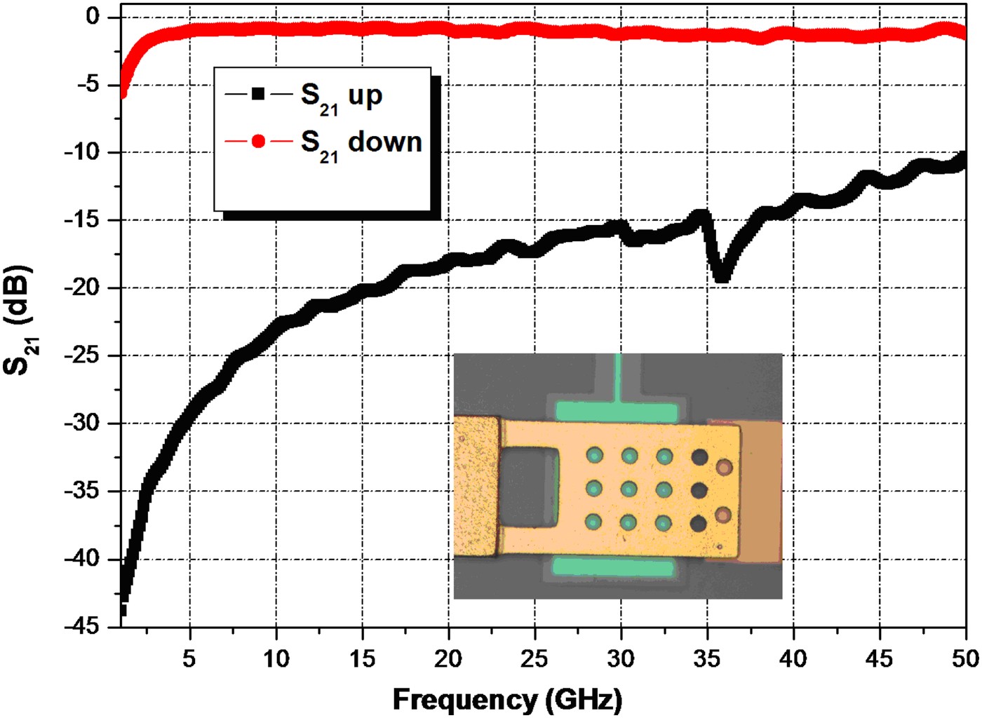
Figure 5 shows the performances obtained for the ohmic series switch in up and down state: insertion loss of circa 1 dB and isolation higher than 15 dB in the frequency band 5–35 GHz have been measured.

Fig. 5. S21 parameter for ohmic-cantilever switch in the “on–off” state.
Such a pretty high-insertion loss in down position (i.e. “on state”), is somewhat due to the series DC-blocks and partially due to the non-zero contact resistance of the MEMS switch.
In order to better quantify the contribution of the contact resistance, the latter has been measured by using a DC setup. Values around 9 Ω have been obtained, indicating that are needed technological and design improvements, such as the optimization of the contact dimple area, height, number, material, and roughness, in the future developments.
To preliminary evaluate the process yield of our ohmic series switch fabrication process we measured the on-wafer distribution of linear performances for these RF-MEMS. All device samples have been RF tested resulting in 62.5% working devices. As presented in Fig. 6, we observed a variation of 7 and 30% for insertion loss and isolation, respectively. Such a spread in the isolation performances could be probably related to the gradient residual stress of the cantilever beam and therefore it is mandatory to improve the beam metallization scheme and sacrificial layer removal in the future process optimization.

Fig. 6. Best and worst S21-parameter for ohmic switch in the “on–off” state.
The performances of the shunt capacitive air-bridge MEMS switches are displayed in Fig. 7. An insertion loss of about 1 dB, and isolation higher than 15 dB in the frequency band 20–45 GHz have been obtained. Also for the capacitive MEMS a pretty high loss has been observed. In this case this is not due to any contact resistance but the loss seems to be dominated by the DC-blocks loss. Preliminary measurements of the CPW lines with and without DC blocks let estimate a DC-block loss contribution of about 0.6 dB @20 GHz. This value is two times higher than the simulated one mainly because no dielectric loss has been accounted in the simulations.

Fig. 7. S21-parameter for pure capacitive switch in the “on–off” state.
In the On-state the switch shows a peak of maximum isolation around 42.5 GHz, corresponding to a Cdown/Cup ratio of four. This indicated the presence of surface roughness and bridge-shape factor, which prevent the intimate contact between the movable membrane and the RF line underneath.
In order to obtain a more repeatable and higher down-state capacitance value a Ti/Au metal plate (also called floating metal [Reference Rottemberg, Jansen, Fiorini, De Raedt and Tilmans10]) has been deposited on the top the SiN dielectric, below the suspended membrane. Figure 8 depicts the performance of a similar shunt switch with the floating metal:
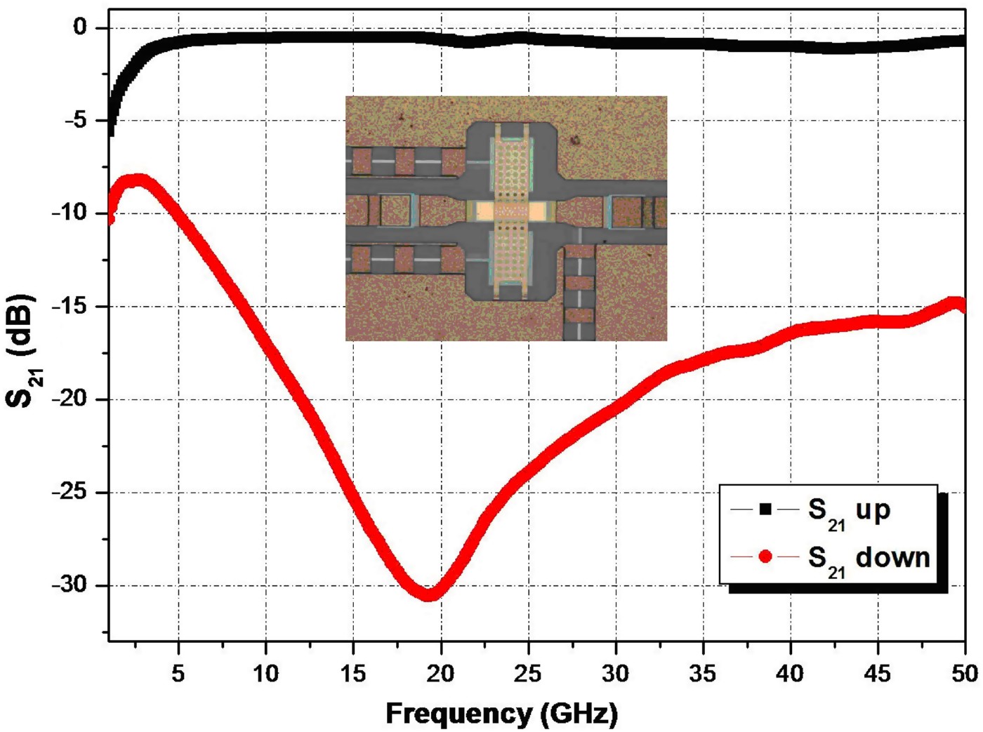
Fig. 8. Capacitive switch S21-parameter with floating metal in “on–off” state. C on/C off ratio
An insertion loss less than 1.5 dB, and isolation higher than 15 dB in the frequency band 10–50 GHz.
Note that the floating metal does not introduce any additional loss in the Off-sate (up-state); on the other hand, in the On-state it allows to realize higher C down/C up ratio up to 15. These results confirm that without floating metal electrode we are not able to obtain a planar contact between the metallic membrane and SiN dielectric layer. The main drawback is that sometimes it is difficult to maintain stable contact between the membrane and the floating electrode most likely due to electrostatic charge accumulation. In summary, the actuation voltages needed to switch the ohmic cantilever MEMS are 30–40 V, whereas for air-bridge capacitive membrane MEMS are 50–60 V. Respect to the actuation voltages, it is worthwhile to mention that the values utilized both for capacitive and ohmic RF-MEMS are fully compliant to the typical DC bias requirement for GaN-HEMT applications and this compliance could be particularly useful for future GaN-based T/R module.
IV. GaN-HEMT PERFORMANCE
Discrete GaN-HEMTs, with a gate periphery (Wg) equal to 1 mm (10 µm × 100 µm), have been utilized as test device for RF active device performance evaluation.
S-parameters of GaN-HEMT devices have been measured to evaluate the small-signal performance in terms of gain (G max and H21) and maximum operating frequency (F max and F t). Taking into account the device power ratings, the S-parameters have been measured with a maximum test frequency of 40 GHz and a typical bias point of V DS = 10 V and I DS = 20% I DSS. As shown in Fig. 9, we have obtained for the GaN-HEMT devices, fabricated with integrated RF-MEMS, a small-signal performances, that is, F t and F max, comparable to the our standard GaN/SiC HEMT process [Reference Ciccognani11]. In fact the small reduction observed in F t is caused mainly to higher gate-source capacitance observed in our DC testing and not to the change introduced during the MEMS fabrication process.

Fig. 9. GMax (continuous line) and H21 (dotted line) measured for GaN HEMT-MEMS on Silicon (black) compared to our standard GaN/SiC HEMT (red).
To evaluate output power performances, an extensive load-pull campaign has been completed on these test devices. Such measurements have been performed in pulsed bias condition through the pulse duration of 100 µs and the 10% duty cycle. The non-linear characterization has been performed at 3 GHz with a pulsed drain bias varied from V DS = 20 V up to V DS = 40 V and I DS@20% I DSS.
Such a characterization shows a significant high power densities, circa 6.5 W/mm at 3 dB gain compression @ V DS = 40 V. As for small signal performance, output power results confirm that integration of RF-MEMS with GaN-HEMT device could be achieved without significant deviation from our standard GaN/SiC HEMT performance (Fig. 10), [Reference Ciccognani11].

Fig. 10. Power density obtained for 1 mm gate periphery (10 µm × 100 µm) GaN device for GaN HEMT-MEMS on Si (black line) and a standard GaN/SiC-HEMT (red line).
Although the high drain bias conditions utilized during our test, up to 40 V, it is worth noticing that HEMTs have shown a robust behavior, not affected from leakage or current reduction after test measurements.
V. GaN-LNA PERFORMANCE
The S-parameters of the two LNAs have been measured to evaluate the small-signal performance in terms of gain and noise figure. To maximize the gain and noise performances of the amplifiers, the S-parameters have been measured with a maximum test frequency of 40 GHz and a typical bias point of V DS = 5, 10 e 15 V and I DS = 20% I DSS.
In Fig. 11 we report the two stages LNA gain in the frequency ranges 6–10 GHz varying V DS voltage. The LNA gain for V DS > 5 V is circa 12 dB with a small ripple of 0.5 dB in said band.
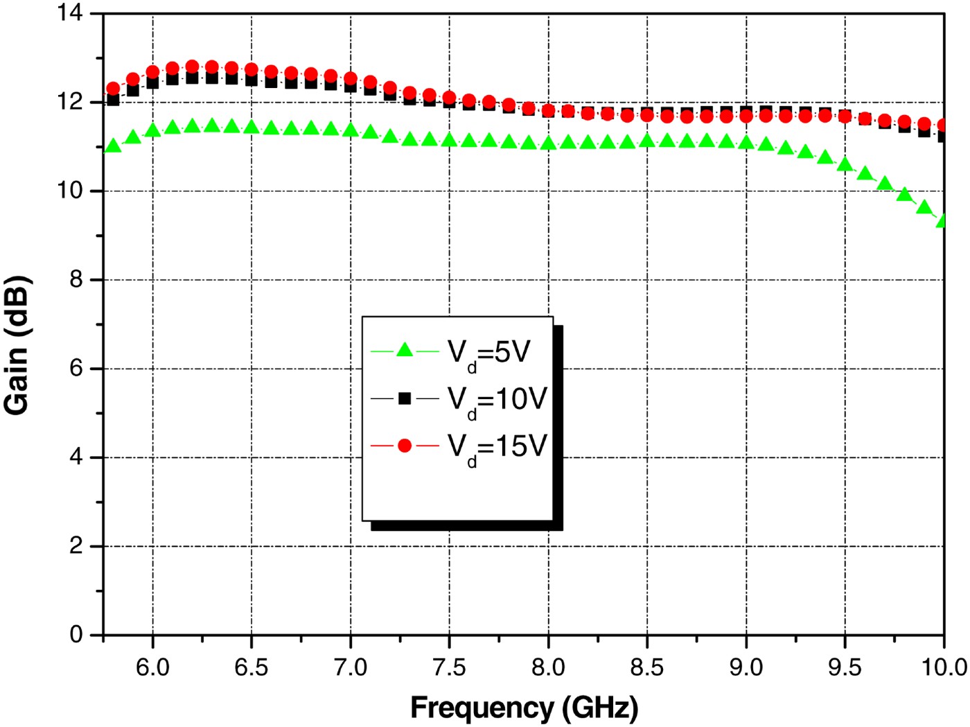
Fig. 11. Two stages LNA gain in the frequency range 6–10 GHz for three different V DS: V DS = 5 V (green); V DS = 10 V (black); V DS = 15 V (red).
As a significant LNA figure of merit, [Reference Bettidi12], we have evaluated the dissipated power in CW condition obtaining 0.6 W and 1 W for V DS = 10 V and V DS = 15 V, respectively.
In Fig. 12 the three stages LNA gain are shown in the frequency ranges 7–10 GHz, varying V DS voltages. The LNA gain continuously increase varying V DS and for V DS =15 V is circa 12 dB in the center band with a large ripple of 3 dB in the band limit.

Fig. 12. Three stages LNA gain in the frequency range 6–10 GHz for three different V DS: V DS = 5 V (magenta); V DS = 10 V (blue); V DS = 15 V (cyan).
For the three stages the dissipated power in CW condition is 1 W and 1.8 W for V DS = 10 V and V DS = 15 V, respectively.
On the basis of these results we have identified as more performing MMIC the two stages LNA. On-wafer noise measurements have been performed exploiting the noise figure analyzer Agilent N8975A.
The two stages LNA noise figure and correspondent gain are reported in Fig. 13, in the frequency center band. In particular, in the frequency range 7–8.5 GHz, we have measured a very flat Gain, circa 12 dB, and NF, circa 4 dB, for V DS = 10 V (best results are 2-stages LNA with NF less than 1.8 dB with 18 dB gain in X-Band on GaN/SiC [Reference Krausse, Quay, Kiefer, Tessmann, Massler and Leuther13]).

Fig. 13. Two stages LNA gain (black line) and NF (red line) for V DS = 10 V and I DS = 20% I DSS.
Such results show:
1) Two-stages LNA: a noise figure two dB higher than our standard GaN/SiC HEMT process [Reference Bettidi, Corsaro, Cetronio, Nanni, Peroni and Romanini14]
2) Three-stages LNA: the linear gain is comparable to the 2-stages one
All these issues are related to the passive components models on GaN/Si substrate not yet optimized to properly predict accurately the RF losses up to 10 GHz. As a result, passive components manufactured on the wafer, see Fig. 1, will be characterized in order to model correctly their losses on GaN/Si. By means of such a characterization and modeling activity, we expect to achieve comparable performances obtained for GaN/SiC substrates.
VI. CONCLUSION
Fully integration of GaN HEMT-MMIC and RF-MEMS has been shown on GaN/Si substrates. The whole process flow and the relevant RF results demonstrate the capability to integrate GaN LNA and RF-MEMS devices in a single process obtaining very encouraging results for both functions. Further improvements in the modeling and in the MEMS layout design, will rapidly bring towards new full integrated MMIC/RF-MEMS functionality. On the basis of these results GaN/Si technology could represent a viable solution to develop high-performance and low-cost applications.
ACKNOWLEDGEMENT
This research activity is partially funded by national research program FIRB RBIP068LNE.
 Flavia Crisplodi was born in May 1979. Master Degree in Physics at University of Rome “La Sapienza”, September 2004. Ph.D. in Physics at University of Modena on February 2009.
Fellowships at University of Perugia, 2009. Research Contract at “OPTEL” Reasearch Institute in Brindisi, 2010. Post Doctoral Fellowship at University of Roma “Tor Vergata”, 2010–11.
 Simone Lavanga was born in Rome on 1973. Master Degree in Physics, specialization in Condensed Matter Physics, obtained at the University of Rome LA SAPIENZA (July1999).
PhD in Microsystems Engineering obtained at the University of Rome TOR VERGATA (March 2003). Present position since 2001: MMIC Process Development Engineer in the GaAs Foundry division of the company Selex Sistemi Integrati S.p.A.
 Paolo Romanini was born in Rome, Italy, on 1973. He received the Degree in Physics from the University of Rome La Sapienza. Since 2002, he has been with Selex Sistemi Integrati S.p.A., Rome, Italy. His current research interests are processing, and characterization of III–V devices, high-resolution lithography, thin-film deposition, and etching techniques. In particular, he is involved with AlGaN–GaN HEMT technology for high-power high-frequency applications.
 Antonio Nanni was born in Pavia, Italy, on May 27, 1978. He received the M.S.Eng. degree in electronics engineering (summa cum laude), in 2004, and the Ph. D. degree in Telecommunications and Micro-Electronic at the University of Roma Tor Vergata. Since 2009 he is working at Selex Sistemi Integrati and his current work is focused on noise and power characterization and modeling of microwave active devices for high-performance applications and extreme operating conditions. During 2005 GAAS Conference, Antonio Nanni won a fellowship.
 Alessio Pantellini obtained his M.S. degree in Electronic Engineering (with honors) in 2007 from “Roma Tre” University, Rome, Italy. He is actually a Ph.D. student of “Roma Tre” University on the area of “Electronic: from nanostructures to systems”, and he joined Selex Sistemi Integrati from the beginning of 2009, where his research focus on design, fabrication, characterization, and development of GaN/GaAs-based devices, especially power switch devices.
 Claudio Lanzieri is currently the head of GaAs Foundry of Selex Sistemi Integrati S.p.A.He has been working in the GaAs technologies since ‘80. Since 2005 he is responsible for the production in Selex of GaAs MMICs and the development of GaN processing techniques.
 Paola Farinelli was born in Assisi, Italy, on September 19, 1978. She received the Laurea degree (with distinction) in electronic engineering from the University of Perugia, Italy, in 2002. In 2002 she joined the Department of Electronic and Information Engineering of the University of Perugia as a PhD student. In 2003 she conducted research work at the “Institut de Recherche en Communications Optiques at Microondes (IRCOM)”, Limoges University, (France). From November 2004 to May 2005 she has been a visiting researcher at VTT Millilab (Finland). In January 2006 she received the PhD degree and she is currently working at the University of Perugia as a contract researcher. Her research activity includes the electromagnetic modeling and design of reconfigurable RF-MEMS devices such as SPDT switches, phase shifters, power dividers, filters.
 Leonardo Rizzi received the Master of Science degree in Microelectronic Engineering from Politecnico di Bari, Italy, in 2002, with a thesis on “Characterization of pixel detector analog front-end of Alice experiment at CERN-LHC”. In 2002–03 he cooperated in INFN – section of Bari, Italy, within the Silicon Pixel Detector Group, where he developed packaging techniques of silicon pixel detectors with electronic front-end and the subsequent electrical characterization of the pixel matrix analog section. Since July 2003 he's been employed in Optel, Brindisi (Italy), a national consortium of research in microelectronic of III-V group semiconductors. These researches, for industrial purposes, were developed in the framework of microelectronics fabrication technology of sensors (gas, pressure, and temperature), micromachining semiconductor (silicon and silicon carbide) and ultimate in RF-MEMS circuits. This latest research field includes microwave/millimeter-wave devices integrated with high-density power amplifiers devices as P-HEMT on gallium nitride, for X-band and K-band radar communication technology.