


Introduction
The need for low-profile high-gain antennas has been the motive for the rapid development in artificial surfaces. Perfect electric conductors provide poor backing-ground performance for horizontal antennas. Perfect magnetic conductors (PMC) on the other hand provide in-phase images for horizontal radiators. Hence, the antenna can be placed arbitrarily close to it, which eliminates the large physical separation. PMCs do not exist in nature; however, their performance can be realized in a limited frequency range by artificial surfaces [Reference Sievenpiper, Zhang, Broas, Alexopolus and Yablonovic1–Reference Mosallaei and Sarabandi3]. One of those structures is artificial magnetic conductors (AMCs), which are periodic structures that provide high impedance behavior for normally incident plane waves. In case of oblique incidence, the surface can be considered alternatively as an electromagnetic band gap (EBG) structure that suppresses surface modes [Reference Yang and Rahmat-Samii4].
Current AMCs either exhibit large pitches, which compromise the homogeneity of the surface [Reference Wu and Yang5], or bulky size, which results in either thick substrates or large spacing between the AMCs and the antennas [Reference Saad and Ford6–Reference Kamoda, Kitazawa, Kukutsu and Kobayashi8]. To miniaturize their sizes, several techniques, such as interdigital capacitors [Reference Malekpoor and Jam9, Reference de Cos, Álvarez, Hadarig and Las-Heras10], lumped components [Reference Liu, Ford and Langley11], and interleaved conductors [Reference Vallecchi, Langley and Schuchinsky12], were investigated.
The position of the antenna with respect to the AMC is also a critical design parameter. While theoretically the antenna can be placed as close as desired to the AMC, practically there is a significant coupling between the antenna and the constituent unit cells, which alters the driving impedance of the antenna. To reduce this coupling, the height separating the antenna and the surface should increase at the cost of the profile of the assembly.
The placement of the AMC with respect to the substrate also introduces additional losses and causes a degradation in the radiation efficiency of the antenna, e.g. in complementary metal–oxide–semiconductor (CMOS) technology, it was shown in [Reference Ibrahim, El-Henawy and Safwat13] that conventional AMCs could not achieve the loss performance of a quarter wavelength grounded substrate.
To mitigate the losses of the silicon substrate in CMOS technology, one of the authors recently proposed a polarization-independent AMC. The unit cell consisted of a dielectric sandwiched between two metal patches placed on the top metal layers [Reference Ibrahim, El-Henawy and Safwat13]. That configuration, which was recently modeled in [Reference Presse and Tarot14], provided large capacitance, confined the electric field in the dielectric and reduced the fringing field in the silicon substrate. Moreover, and due to the combination of the antenna and AMC, a dual band operation was obtained, and it was possible to merge these two bands into a single wide one. In order to conform to the Design Rules Check, the square patches were replaced by square rings, which did not compromise the performance. This shows that the methodology can be adopted for different unit cell geometries. Unfortunately, it was not feasible to scale down the dimensions in [Reference Ibrahim, El-Henawy and Safwat13] to low frequencies, as the substrate thickness had to be close to λ s/4, where λ s is the wavelength of the plane wave in the substrate, and the concept was not confirmed experimentally.
This paper proposes a stack layer that allows the implementation of the double-layer AMC at a low frequency (2 GHz) on a lossy substrate. The center frequency is chosen away from the crowded 2.4 GHz ISM band, to mitigate the interference in the measurements as some of the testing was performed outside the anechoic chamber. The proposed structure is mechanically robust, and it is compact as it has a thickness of 0.051 λ, the free space wavelength. To the authors’ knowledge, this stack layer does not exist in the literature as it combines different substrates of different electrical characteristics. This paper also utilizes this proposed surface in the realization of a dipole antenna that has a high radiation efficiency on FR4 substrate, as shown in Fig. 1.

Fig. 1. Metal layers and dielectrics of the proposed structure. (a) Isometric. (b) X–Z cross section. (c) Y–Z cross section. (b) and (c) are zoomed to the feeding to illustrate the gaps between the patches.
Dipole above double-layer AMC
AMC design
Conventional AMC, shown in Fig. 2(a), consists of square patches on conductor-backed substrate. The pitch is p, the square patch is of side length L p, and the substrate thickness is h 1. The equivalent circuit model when the AMC is excited by a normally incident plane wave is depicted in Fig. 2(b) [Reference Ibrahim, El-Henawy and Safwat13]. The conductor backed-substrate is modeled by a short-circuited lossy transmission line, and the metal patches are modeled as a lumped capacitor, C, whose expression was provided in [Reference Luukkonen, Simvoski, Granet, Goussetis, Lioubtchenko, Raisanen and Tretyakov15]. The substrate is characterized by the following parameters, ε0εr is the permittivity of the substrate, tan δ is the loss tangent, μ 0 is the free space permeability, and T SUB is the substrate thickness. Hence, the input impedance at the surface η in is given by (1)–(3):
 $$\eta _{in} = \eta _2\tanh \lpar {\gamma_2T_{SUB}} \rpar $$
 $$\eta _2 = \; \displaystyle{{\,j\omega \mu _0} \over {\gamma _2}}\; $$
 $$\gamma _2 = \; j\omega \sqrt {\mu _0\varepsilon _0\varepsilon _r} \sqrt {1-j\,{\rm tan}\; \,\delta} $$
where ω is the angular frequency, and η 2 (the intrinsic impedance) and γ 2 (the complex propagation constant) are given by (2) and (3), respectively.

Fig. 2. Conventional AMC. (a) Unit cell layout. (b) Transmission line model when the AMC is excited by a normally incident plane wave. (c) Analytical versus EM simulated reflection coefficients. The solid lines represent the EM simulations and the dotted lines represent the analytical solution. The EM simulations are carried on by HFSS V.15. The simulation environment is a box which encloses the unit cell, with two opposing lateral faces assigned as perfect-E and the other two lateral sides perfect-H, and the top face assigned a wave port to ensure the normal incidence of a plane wave.
Equations (1)–(3) indicate that increasing the thickness of the substrate increases the losses as it is equivalent to extending the length of the lossy transmission line in the circuit model. Figure 2(c) compares the electromagnetic (EM) simulations and the analytical results for a unit cell realized on FR4 substrate (ε r = 4.4 and tan δ = 0.02), with p = 12.5 mm, and for three values of the substrate height h 1, 6, 7.5, and 9 mm. For each value of h 1, L p is adjusted to maintain the resonance at the design frequency, 2 GHz. The EM simulations exhibit an opposite trend and the losses decrease by increasing the thickness of the substrate. This can be explained as there are three sources for the losses; the propagation losses modeled by the lossy transmission line, the losses due to the fringing of the electric field between the patches in the same layer, which is illustrated by the resistor R f in the proposed model depicted in Fig. 2(b), and finally, the fringing of the electric field between the patches and the ground plane, which reduces as the substrate thickness increases.
To mitigate for the losses due to fringing, this paper proposes placing a low-loss substrate above the FR4 and replacing the single layer of patches by two layers of patches that sandwich a low-loss dielectric as shown in Fig. 3. The use of the double-layer AMC provides a large capacitance, whose expression was given in [Reference Presse and Tarot14], leading to the confinement of the electric field in the low-loss substrate and reducing the fringing of the electric field to the ground. Meanwhile, it keeps the FR4 platform as it offers several advantages such as its low cost and abundance in contrast to the high cost of the low-loss substrates, moderate value of dielectric constant, which provides compactness compared to the air substrates with spacers. In addition, the air backed substrates, particularly thin ones, are more prone to bending against pressure, which causes deviation in the performance and may lead to their fracture, hence this structure is more mechanically reliable.

Fig. 3. The proposed double-layer unit cell.
To highlight the differences between the single- and double-layer AMCs, three unit cells are designed and simulated on ANSYS HFSS ver. 15 using an incident plane wave and the corresponding perfect electric and perfect magnetic boundary conditions. The unit cells are designed to provide a high impedance behavior with 0° reflection phase at 2 GHz.
The bandwidth of operation is defined to be the frequency range at which the reflection phase lies between −90 and 90°. Table 1 shows the dimensions of the cells in comparison. The first case (AMC 1) is a double-layer AMC with a pitch size p = 12.5 mm. The FR4 thickness, h 1, is 3 mm, the low-loss substrate is Arlon DiClad 880 (ε r = 2.2 and tan δ = 0.0009) of thickness, h 2, 0.508 mm. This substrate, which should be very thin to maximize the capacitance between the two layers of patches, is chosen as it is the thinnest available at our facility. For the other two cases, single-layer AMCs are considered. AMC 2 has the same FR4 thickness, h 1, of 3 mm, and p and L p are set to 17.5 and 17.45 mm, respectively, to obtain the resonance at 2 GHz. For AMC 3, h 1 is set to 6 mm, p is kept unchanged at 12.5 mm, and L p is set to 12.33 mm to keep the same resonance frequency. To include the conductor losses, the conductors are modeled as copper traces of 17.5 µm thickness.
Table 1. Dimensions of the investigated AMCs (in mm).

Figure 4, which shows the simulated reflection coefficients of the unit cells, confirms the predictions. Comparing AMC 1 and AMC 2, the two unit-cells have the same substrate thickness, i.e. the same inductance, therefore for the same resonance frequency the two configurations of patches provide the same capacitance. AMC 1 provides this capacitance while it consumes only half the area. Moreover, the magnitudes of the reflection coefficients indicate higher losses of 2.23 dB in the single-layer structure (AMC 2) compared with 0.59 dB of the double-layer structure (AMC 1).

Fig. 4. Reflection coefficients of the investigated unit cells. (a) Magnitude. (b) Phase.
Comparing AMC 1 and AMC 3, the reflection phase shows a wider bandwidth of operation provided by AMC 3. This is due to the larger inductance of the thicker substrate. However, this improved bandwidth comes at the cost of a larger profile of almost twice the thickness. Like AMC 2, AMC 3 exhibits higher losses of 1.14 dB compared with the 0.59 dB of AMC 1. It is worth noting that the lower losses of AMC 3 compared with AMC 2 are due to the reduced fringing electric field between the ground plane and the capacitive layer as aforementioned. The performance of the double-layer AMC for three different values of the FR4 substrate thickness, h 1 = 3, 4.5, and 6 mm, is also investigated. Figure 5 shows that increasing the substrate thickness leads to a marginal improvement in the losses. As the thickness increases from 3 to 4.5 mm there is an improvement of 0.15 dB only. Further increment leads to the saturation of the diminishing of the losses. This demonstrates that the large capacitance introduced by the double-layer structure shifts the main source of losses from the fringing field to the ground to be the fringing fields between the patches. Figure 5(b) also shows that increasing the substrate thickness increases the operational bandwidth as well. Large substrate thickness can be realized by stacking layers of FR4 substrates upon each other. Unfortunately, this may lead to rapidly diminishing the improvement in the losses, imperfections in the mechanical fastening of the stack, and the presence of air gaps between the layers. To mitigate these effects and facilitate the feeding of the antenna through the AMC, the 3-mm thickness of FR4 is chosen with a bandwidth of 280 MHz and 0.59 dB losses. Increasing the thickness of the FR4 substrate causes an increase in the weight. The chosen small thickness provides a reliable mechanical design as the weight of the antenna above the AMC is placed on the connector as will be shown in later sections.

Fig. 5. Reflection coefficient of the proposed double-layer AMC on different substrate thickness. (a) Magnitude. (b) Phase.
AMC loaded dipole
Placing the dipole at the same metal layer as the AMC connects the unit cells. Hence, a dielectric layer that separates the dipole form the AMC is inserted. This layer is chosen to be an Arlon Foam Clad substrate with a thickness, h 3, of 2.692 mm, and a permittivity, ε r, of 1.2, as this small permittivity will not distort the dipole radiation pattern. The design procedure of the AMC loaded dipole starts by designing the dipole and the AMC, separately. A co-design step then comes on, where the dipole and AMC are combined, and the dimensions of the dipole are tuned to achieve a wideband operation. These steps, which are depicted in Fig. 6, are briefly described hereafter.
Step 1: All metal layers are removed, and a 2 GHz dipole antenna is designed on the top metal layer (metal layer 5). Figure 7 shows that a good matching is achieved at 100 Ω port impedance when L dip = 6.6 cm and W dip = 6 mm.
Step 2: The AMC surface, described in the previous section, is added. The number of the unit cells is set to 12 × 8 so that the surface area is large enough compared with the dimensions of the dipole.
Step 3: Two vias that go through the whole structure are inserted to feed the dipole. These vias are excited differentially at metal layer 1 using a 100 Ω-lumped port. The AMC loaded dipole provides a dual band operation. They are centered at 2 and 2.34 GHz and they do not overlap. The dimensions of the dipole are then optimized to merge these two bands into a single wideband one as shown in Fig. 7. The optimized dimensions are L dip = 6.8 cm and W dip = 8 mm, and the average input resistance across the band of operation is 100 Ω.
Step 4: A balun that connects the dipole to the SMA connector is inserted on the lowest metal layer (metal layer 1), as shown in Fig. 1. The substrate is FR4 of thickness, h 0, 1.5 mm. The balun provides an output differential impedance of 100 Ω to match the dipole over the entire operating bandwidth of the antenna and has an input impedance of 50 Ω. Figure 8 shows its design [Reference Zhang, Guo, Ong and Chia16], while Table 2 depicts its dimensions. The EM simulations show that this balun provides an impedance bandwidth from 1.5 to 2.7 GHz with an output amplitude imbalance better than 0.26 dB and phase imbalance better than 3° across the band of operation. Figure 7 shows the performance of the AMC loaded dipole after adding the balun. The bandwidth extends from 1.89 to 2.2 GHz. The discrepancy between the EM simulations of the AMC loaded dipole with and without balun is due the fluctuations of the output impedance of the balun.

Fig. 6. Design procedure of the proposed dipole above AMC.

Fig. 7. Magnitude of the reflection coefficient of the dipole above AMC at design steps 1, 3, and 4.

Fig. 8. Schematic of the wideband feeding balun. The red square corresponds to 100 Ω.
Table 2. Dimensions of the balun (in mm).

Fabrication and measurements
Figure 9 shows the fabricated structure. The feeding vias provide two functions, the first is to excite the dipole, and the second is to provide alignment between all the layers, both in their relative positions to each other and their orientation, which is demonstrated by the cross sections of the structure in Figs 1(b) and 1(c). To minimize the misalignments between the different layers, the through-holes are drilled in each layer individually. After that, the stack is aligned and examined for mismatches. The vias are then inserted through the stack which holds the positions of the layers relative to each other. The presence of small shifts can be taken into consideration in the design. In this case, wider through-holes are drilled and the vias are replaced by thicker ones which is not detrimental to the frequency response of the antenna at low frequencies. Figure 10 depicts the measured reflection coefficient. It exhibits a 10-dB impedance bandwidth from 1.927 to 2.267 GHz (16.2%) and shows a good agreement with the simulated one, also shown in Fig. 10. The minor discrepancy between the simulations and measurements, which is in the form of a 50 MHz frequency shift, is attributed to the fabrication imperfections. These imperfections include the etching tolerances, misalignments between the patches, deviation in the substrates permittivity, stack layer misalignments, the presence of the air gaps between different layers, and via and soldering parasitic effects. To account for this shift in the measurements of the radiation patterns, they are plotted at the frequency of the first minimum. This frequency is 1.97 GHz in the simulations, while it is 2.03 GHz in the measurements.

Fig. 9. Fabricated AMC loaded dipole. (a) Metal layer 4 before assembly. (b) Metal layer 3 before assembly. (c) Metal layer 5 after assembly. (d) Metal layer 1 after assembly.

Fig. 10. Simulated and measured |S 11| of the proposed AMC loaded dipole antenna.
The measured radiation patterns in Fig. 11 show very good agreement with the simulations. The measured and simulated directivity, shown in Fig. 12(a), are also in a very good agreement. The radiation efficiency, which is measured using the modified Wheeler cap method [Reference Wheeler17, Reference Geissler, Litschke, Heberling, Waldow and Wolff18], is depicted in Fig. 12(b). There is an excellent agreement between measured and simulated ones. The peak simulated, and measured radiation efficiencies are 74.3 and 72.5%, respectively, which correspond to peak gains of 8.19 and 8.1 dB, respectively, across the band of operation. This is larger than that reported in the literature [Reference Yang, Tam, Choi, Che and Hui19–Reference Joshi, Lepage, Sarrazin and Beguad21] as depicted in Table 3, such that at the frequencies corresponding to the maximum gains the antennas are well matched. In addition, the EM simulations with the lossless balun in Fig. 12(b) indicate that feeding the dipole above AMC by the FR4 balun reduces the gain of the assembly by more than 1 dB across the band of operation. These losses in the balun can be mitigated by different feeding configurations, e.g. [Reference Mostafa, Abuelfadl and Safwat22], however they may add more complexity to the design. Figure 12(c) depicts the simulated and measured realized gains, they exhibit very good agreement with peak values of 7.85 and 7.55 dB, respectively. The 3-dB variation bandwidth in the realized gain is from 1.81 to 2.32 GHz in the simulations and from 1.89 to 2.55 GHz in the measurements.
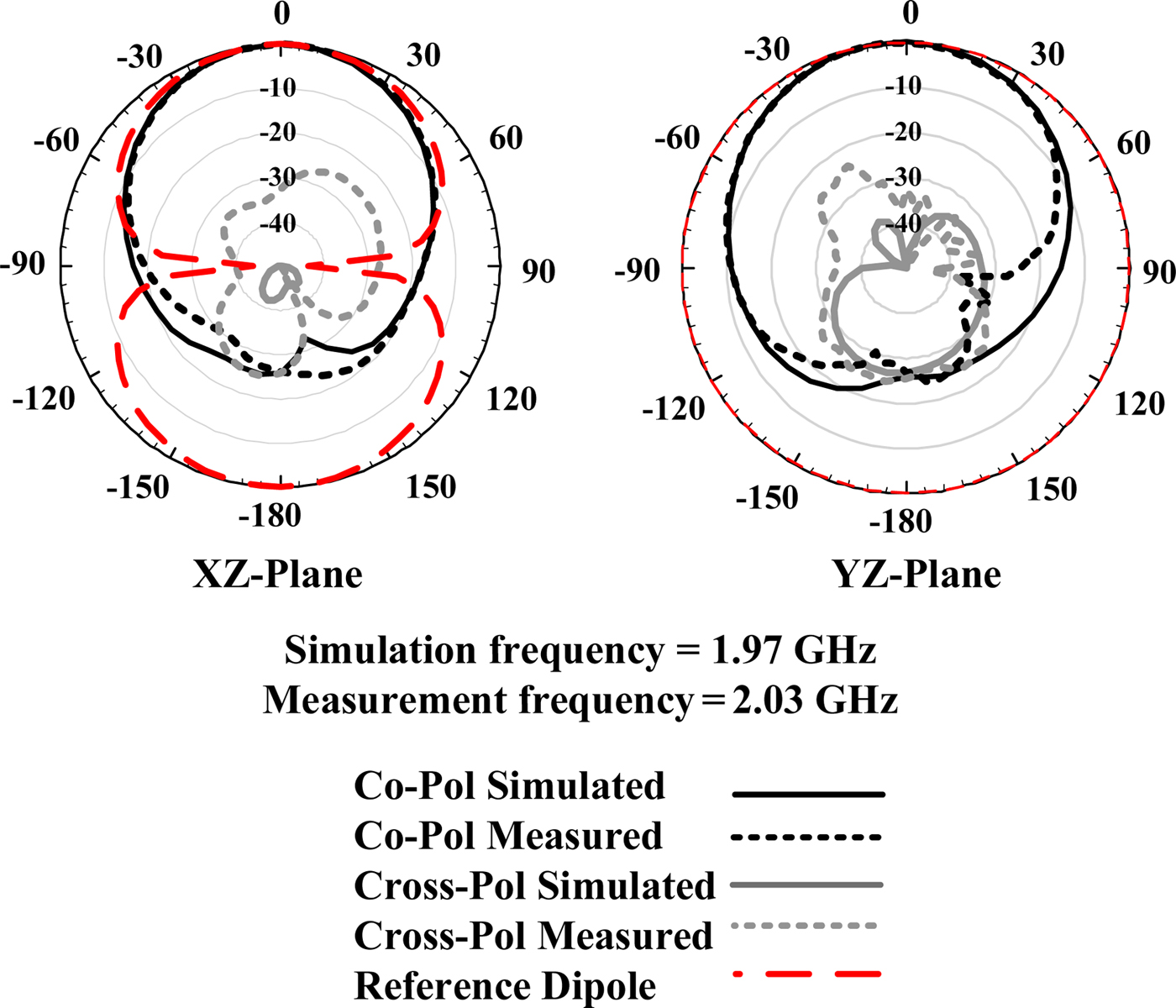
Fig. 11. Simulated and measured radiation patterns of the proposed AMC loaded dipole antenna.

Fig. 12. Simulations versus measurements of the proposed AMC loaded antenna. (a) Directivity. (b) Efficiency. (c) Realized gain.
Table 3. Comparison with relevant work.

Conclusion
In this paper, a methodology for the design of wide-band high-gain low-profile antennas on lossy substrates in the low frequency range was proposed. The methodology can be adopted for different unit cell geometries, as the introduction of the AMC layer controls the fringing fields and the losses in the commercial PCB substrate. A high efficiency antenna was implemented by placing a dipole above a double-layer AMC. The dipole was fed by a 50 to 100 Ω balun. The fractional operating bandwidth achieved the value of 16.2%, 1.927 to 2.267 GHz, while the peak gain was 8.1 dB. This gain would increase to 9.56 dB if a lossless balun was used as proved by the EM simulations. The whole assembly had a small profile of λ × 0.67λ × 0.051λ, where λ is the free space wavelength at 2 GHz. The structure was fabricated, and a very good agreement was achieved between the simulations and measurements.
Author ORCIDs
Amr M.E. Safwat 0000-0001-5273-9307.
Acknowledgement
This project was supported financially by the Science and Technology Development Fund (STDF), Egypt, Grant No. 14933.
 Mohamed A.G. Elsheikh was born in Cairo in 1993. He received his B.Sc. (with honors) degree in electrical engineering from Ain Shams University, Cairo, Egypt, in 2016. Since his graduation, he was appointed as a Teaching/Research Assistant by the Faculty of Engineering, Ain Shams University. His research interests include passive and active microwave circuits, antennas, and novel electromagnetic materials and devices.
 Amr M.E. Safwat received his B.Sc. and M.Sc. degrees in electrical engineering from Ain Shams University, Cairo, Egypt, in 1993 and 1997, respectively, and his Ph.D. degree in electrical engineering from the University of Maryland, College Park, MD, USA, in 2001. From 2001 to 2002, he was with Cascade Microtech Inc., OR, USA. In 2002, he joined the Electronics and Communication Engineering Department, Ain Shams University, where he is currently a full professor and department chair. His current research interests include metamaterial, microwave passive planar structures, and microwave photonics. Dr. Safwat was a recipient of the Egyptian encouragement state prize for engineering sciences, in 2007 and 2014, and the first class medal of excellence from the president of Egypt in 2017.
 Hadia El-Hennawy received her B.Sc. and M.Sc. degrees from Ain Shams University, Cairo, Egypt, in 1972 and 1976, respectively, and her Doctorate of Engineering (Dr.-Ing.) degree from the Technische Universitat Braunschweig, Braunschweig, Germany, in 1982. Since 1992, she has been a Professor of communication engineering with the Electronics and Communications Engineering Department, Ain Shams University. In 2004, she became a Vice-Dean for graduate study and research. In 2005, she became the Dean of the Faculty of Engineering, Ain Shams University. Her research interests include microwave devices and subsystems, as well as filters and antennas for modern radar and wireless communications applications.


