Introduction
Design of wideband antennas is no-doubt, a research topic of high interest in the field of wireless communications. Various types of wideband antennae, from fractal to monopole, from defected ground structures (DGS) to slotted geometries, etc., designed by antenna researchers all over the globe, have gained huge popularity in this field. To overcome the common disadvantage of multipath fading and to utilize the advantage of diversity of pattern, Multiple-Input-Multiple-Output (MIMO) technology had been proposed. Later, it was combined with ultra-wideband (UWB) technology to achieve the advantageous features of both. The MIMO technology, however, suffers from the serious disadvantage due to the mutual coupling effect between the different radiating structures located in vicinity. The effect tends to become more severe with the increase in compactness of the structure. Hitherto, decoupling structures of various types have been presented in articles [Reference Mak, Rowell and Murch1–Reference Ren, Hu, Yin and Fan5] for reducing the coupling effect among the adjacent radiating elements. Different types of decoupling elements and floating parasitic structures have been proposed in these works. However, the space occupancy is large and the antenna configuration in most cases become much complex. Moreover, for eliminating the interferences arising from systems with narrow frequency bands like WLAN (5.15–5.85 GHz) and WiMAX (3.3–3.7 GHz), various effective frequency band-notching structures have been proposed by researchers in antenna design. Band-notched features can be realized by incorporation of arc-shaped slots [Reference Chacko, Augustin and Denidni6] or Rectangular Complementary Split Ring Resonator (RCSRR) slots [Reference Gao, He, Wei, Xu, Wang and Zheng7] or by insertion of open-ended stubs in the antenna element [Reference Lee, Kim, Ryu and Woo8]. A highly efficient UWB–MIMO antenna having “G-shaped” structure with band-notched feature has been presented in [Reference Toktas9]. In [Reference Li, Chu, Li and Xia10] a MIMO diversity antenna with multiple frequency band-notched features has been designed using parasitic strips and slots in the radiating element. In most of the aforesaid designs, notches are created by modifying the radiators. Lately, an UWB–MIMO antenna combined with band-notched feature is reported in [Reference Liu, Cheung and Yuk11]. The antenna has a dimension of 22 mm × 36 mm. To the authors’ knowledge, it is one of the tiniest UWB–MIMO antennas along with a band-notched feature.
In this paper, an extremely wideband, isolation-enhanced, low-profile MIMO diversity antenna with dual-frequency band-notching characteristics has been studied. The dimension of the proposed design is even tinier than the antenna proposed in [Reference Liu, Cheung and Yuk11]. It has a compact size of only 20 mm × 20 mm (0.08 λ o × 0.08 λ o), where λ o is the wavelength of free space in correspondence to the first resonant frequency, i.e. 1.2 GHz. The antenna designed herein is about 49.5% tinier than the design in [Reference Liu, Cheung and Yuk11]. Table 1 shows the comparison among notable band-notched UWB–MIMO antennas in terms of size and performance.
Table 1. Comparison table of notable band-notched MIMO antennas

Two staircase-shaped radiating elements matched to 50 Ω feed line impedance have been designed to obtain wideband characteristics as well as orthogonal radiation patterns. A RCSRR structure is introduced in each antenna element for obtaining a band-notched frequency centered at 3.5 GHz. A parasitic element, having shape of English letter “T”, has been incorporated in the mid-position, inclined at an angle of 45° for isolation enhancement. Dual “L-shaped” slits have been incorporated in the ground plane for obtaining a second notched-band centered at 5.5 GHz. The successive design stages have been discussed in the next section.
Antenna design and simulation
Three antennas namely, Antenna A, Antenna B, and Antenna C have been designed here. The process starts with the design of Antenna A (Fig. 1), having two radiating structures and a “T-shaped” parasitic strip. Antenna A has a low-profile structure, having a dimension of 20 mm × 20 mm (0.08 λ o × 0.08 λ o). The substrate utilized here is FR-4, which has a depth of h = 1.25 mm and a dielectric constant of ~4.4. The structure possesses two stepped radiators fed by two orthogonally fed microstrip lines matched to 50 Ω impedance. A wave port is defined at the end face of a sub-miniature ver. A (SMA) connector, designed and simulated in CST Microwave Studio Suite™ in order to excite the antenna. The same has been reflected in Figs 1–3. Stepped radiating structures help in generating multiple resonant frequencies, which subsequently come closer to each other forming a wide bandwidth [Reference Cho, Kim, Choi, Lee and Park12]. Compared with conventional center feeding techniques, the proposed offset-feed is helpful in providing a broader impedance bandwidth [Reference Jan and Kao13]. The radiating elements are placed perpendicular to one another for obtaining good isolation and diversity in antenna polarization. Lying between the antenna elements, there is a parasitic structure, which plays a significant role in minimization of the mutual coupling. A parasitic strip having a shape of English letter “T” is placed at an angle of 45° with the antenna elements for minimization of the mutual coupling effect. The “T”-shaped structure has been proven useful in providing enhanced isolation characteristics and was firstly employed in [Reference Toktas and Akdagli14]. The inserted parasitic strip consists of two sections: one portion of the strip is along the diagonal and the other is placed in a direction which is perpendicular to the diagonal strip. Introduction of the parasitic element plays a significant role in isolation enhancement. The surface current flowing from one port to another is obstructed due to the presence of the stub, which acts as a decoupling element, resulting in isolation improvement. Dimensions of the strip have been optimized to achieve desired isolation levels. An isolation level of ≤−20 dB has been obtained. The antenna ground plane with an etched rhombic slot has been placed on the rearmost position of the substrate. This type of ground structure is called a DGS, which helps in control of bandwidth, impedance matching, and surface-wave suppression [Reference Rehman, Sheta and Alkanhal15]. The prime objective of selecting this particular rhombus-like shape is that it yields a comparatively wider bandwidth and lesser tolerance on the alignment of mass for printing purposes.
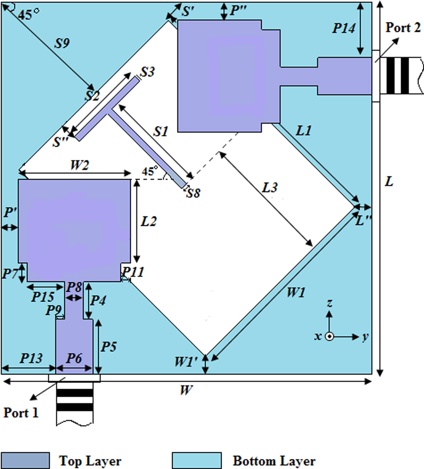
Fig. 1. Layout of UWB–MIMO antenna (Antenna A).

Fig. 2. Layout of single band-notched UWB–MIMO antenna (Antenna B).

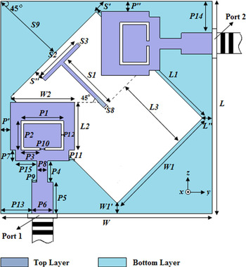
Fig. 3. Layout of proposed UWB–MIMO dual band-notched antenna (Antenna C).
Next, our challenge is to introduce a frequency band notch for the 3.3–3.7 GHz WiMAX band. For this purpose, a “RCSRR” structure has been introduced in the antenna elements. Figure 2 displays Antenna B with a RCSRR slot. The slot length for the notch-band center frequency (f c) can be approximately calculated as,
 $$G = \displaystyle{c \over {4{\rm \;} \,fc{\rm \;} \surd \varepsilon _{eff}}}$$
 $$\varepsilon _{eff} = \displaystyle{{\varepsilon r + 1} \over 2},$$
where “c” represents the speed of light wave in free space, ε eff represents effective electrical-permittivity, and “G”, the outer perimeter of the RCSRR slot is equal to (P1 + 2 P2 + 2 P3). The value of G is calculated to be 13.0 mm, for effectively generating the notch band centered at 3.5 GHz.
Each etched slot behaves like a parallel circuit that acts as a short for the concerned frequency point. It may be noted that the notch frequency can be tuned by varying the dimension of the parameter G, which has been discussed later. Antenna C (Fig. 3) is a modified form of its predecessor Antenna B, with dual-band-notching structures incorporated. The frequency response of Antenna C, i.e. the proposed antenna has been shown in Fig. 4. A rhombic slot has been etched from the ground plane along with dual “L-shaped” slits in order to realize another band notch centered at 5.5 GHz. The effect of introduction of the slits in the ground plane has been discussed in the next section. It may be mentioned here, that the notched band frequency can be adjusted by fine tuning of the length of slits. The simulated frequency responses of the designed antennas, namely Antenna A, Antenna B, and Antenna C have been displayed in Fig. 4. It can be seen that Antenna A is showing an ultra-wide frequency response with no band-notch frequency point(s). Antenna B is showing an ultra-wide frequency response with a single-frequency band notch, whereas, Antenna C, i.e. the proposed antenna is showing an ultra-wide frequency response with dual-frequency band notches. The effect of insertion of the decoupling structure on antenna frequency response (S 21) has been depicted in Fig. 5. After several parametric variations and simulations in an electromagnetic simulation-based software tool CST Microwave Studio™ environment, the antenna geometry has been refined to achieve an extremely wide impedance bandwidth along with two frequency band notches for WLAN frequency band (5.5 GHz) and WiMAX frequency band (3.5 GHz). Simulated results have been compared with measured values in the next section. Detailed parametric specifications of the three antenna structures: Antenna A, Antenna B, and Antenna C have been provided in Table 2.

Fig. 4. Simulated S 11 versus frequency plot of Antenna A, Antenna B, and Antenna C.

Fig. 5. Simulated S 21 versus frequency plot of proposed antenna (Antenna C).
Table 2. Parametric dimensions of Antennas A, B, and C

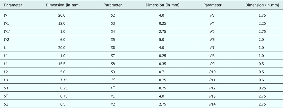
To study the effect of the band-notching structure, i.e. the RCSRR slot, the parameter G is varied and its effect on antenna frequency response has been observed. From Fig. 6 it is noticed that as G increases, the notched-band frequency is lowered. It may be viewed that the change in parameter G does not have a significant effect on the other notched frequency band. For achieving the maximum rejection around a center frequency of 3.5 GHz, the value of G selected, is equal to 13 mm.

Fig. 6. Frequency response of Antenna C for different values of parameter G.
A pair of open-ended slits having a shape of English letter “L”, incorporated in the antenna ground plane, is the cause of generation of the second band notch. The notched band can be finely tuned by altering the slit dimensions. From repeated simulation results, it is found that the parameter of the slit should be selected as, G′ = S4 + S5 = 3.25 mm, for obtaining a notched frequency band centered at 5.5 GHz (Fig. 7).

Fig. 7. Frequency response of Antenna C for different values of parameter G’.
Fabrication, measurement, and analysis
Prototype of the MIMO diversity antenna proposed (Antenna C) is fabricated (Fig. 8). Antenna responses have been measured using a Vector Network Analyzer (VNA) N5-230A. Figure 9 shows the plot of S-parameter (S 11) versus frequency. An extremely wide impedance bandwidth of 18.2 GHz (1.2–19.4 GHz) has been obtained except two frequency band notches centered at 3.5 and 5.5 GHz due to incorporation of effective frequency band-notching structures.
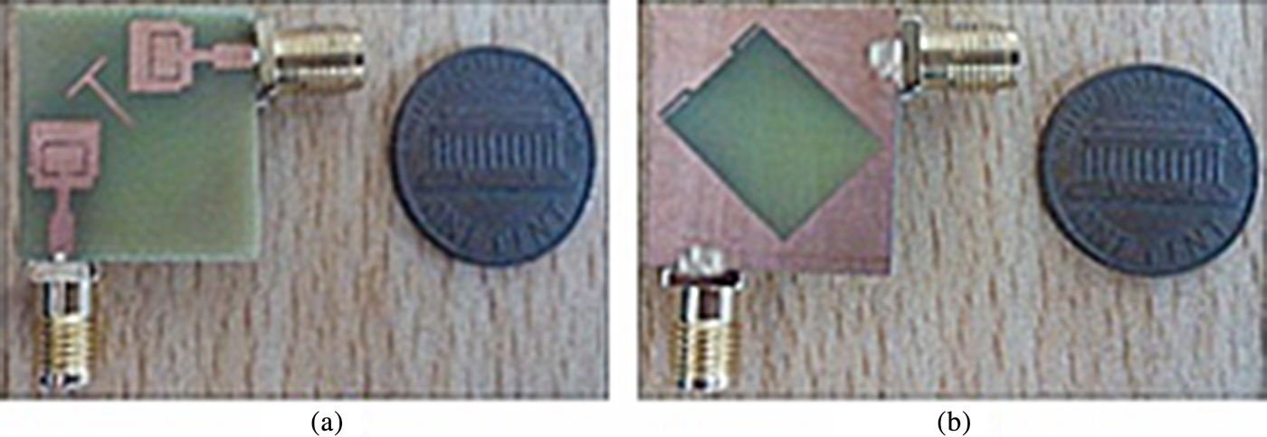
Fig. 8. Fabricated prototype of proposed Antenna C: (a) top view, (b) bottom view.

Fig. 9. S-parameter response of Antenna C (simulated and measured).
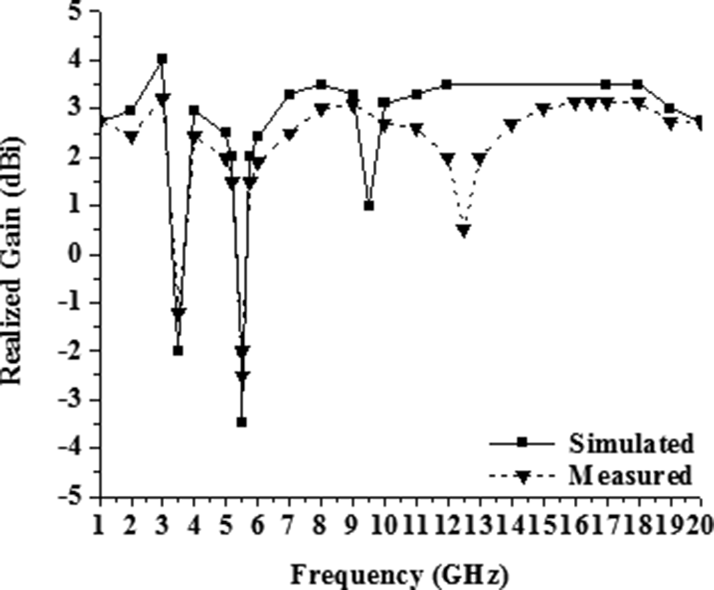
The measured s-parameter (S 21) of the MIMO antenna is depicted in Fig. 9. It is seen that, S 21 is ≤−20 dB throughout the entire bandwidth. Figure 10 displays the realized gain of Antenna C. It may be observed that there is a drastic fall in the antenna gain at the notched frequency bands, whereas, a decent gain has been maintained at the other frequency zones. Impedance matching of an antenna is an extremely crucial matter of concern. To study the impedance-matching characteristics of our designed antenna, we have plotted the input impedance curves (real and imaginary) versus antenna frequency. The input impedance curves of the antenna for the entire impedance bandwidth have been shown in Fig. 11. It can be observed that parallel resonance is exhibited by the imaginary part, while the real part exhibits high resistance approximately around 50 Ω except at the frequency band notches. The effect of the insertion of the parasitic strip can be further explained from the antenna surface current distribution pattern as depicted in Fig. 12. The “T-shaped” strip excites a half wave resonant mode. Due to the incorporation of the parasitic element, the induced surface current is enhanced, thereby creating another path between the radiating structures. As observed from the figure, the current flowing in a direction from Port I to Port II is obstructed by the presence of the stub, which plays a significant role in minimization of the mutual coupling effect between antenna elements. It may be mentioned here that both the ports are matched approximately equal to 50 Ω load impedance.

Fig. 10. Realized gain of proposed antenna (simulated and measured).
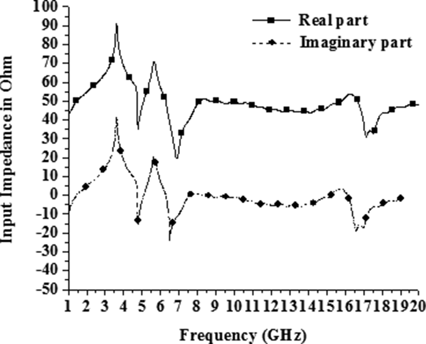
Fig. 11. Measured input impedance curves of Antenna C.
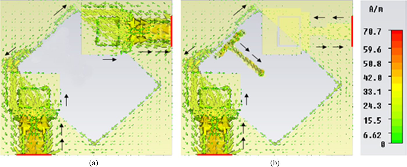
Fig. 12. Surface current distribution pattern of proposed antenna (a) without stub (b) with stub.
The radiation pattern of the staircase-shaped radiating elements for the highest and lowest frequency points has been depicted in Fig. 13 in 3D. The maximum gain obtained is equal to 2.73 dBi. Figure 14 shows the XY, XZ, and YZ planes 2D radiation patterns of the antenna at 1.2 GHz (lowest frequency) and 19.4 GHz (highest frequency) with Port I in excitation mode and Port II matched to 50 Ω load. For symmetry in geometrical structure and for placing the antenna elements at right angles to each other, the radiation patterns of both the ports are somewhat identical rotated by angle of 90°.
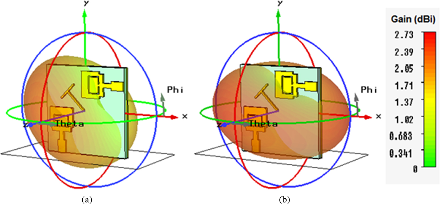
Fig. 13. Simulated 3D radiation pattern of proposed antenna: (a) 01.2 GHz (lowest frequency), (b) 19.4 GHz (highest frequency).

Fig. 14. Measured 2D radiation pattern of proposed antenna at the lowest (01.2 GHz) and highest (19.4 GHz) frequency points.
The antenna surface current distribution pattern at various frequency point(s) has been depicted in Fig. 15. The existence of band-notching structures causes a disturbance in the distribution of antenna surface current as depicted in Figs 15(b) and 15(c), thereby reducing the gain at the notched frequencies below the 0 dBi level: −2.0 dBi at the WiMAX band (3.3–3.7 GHz) and −3.5 dBi at the WLAN band (5.15–5.85 GHz).
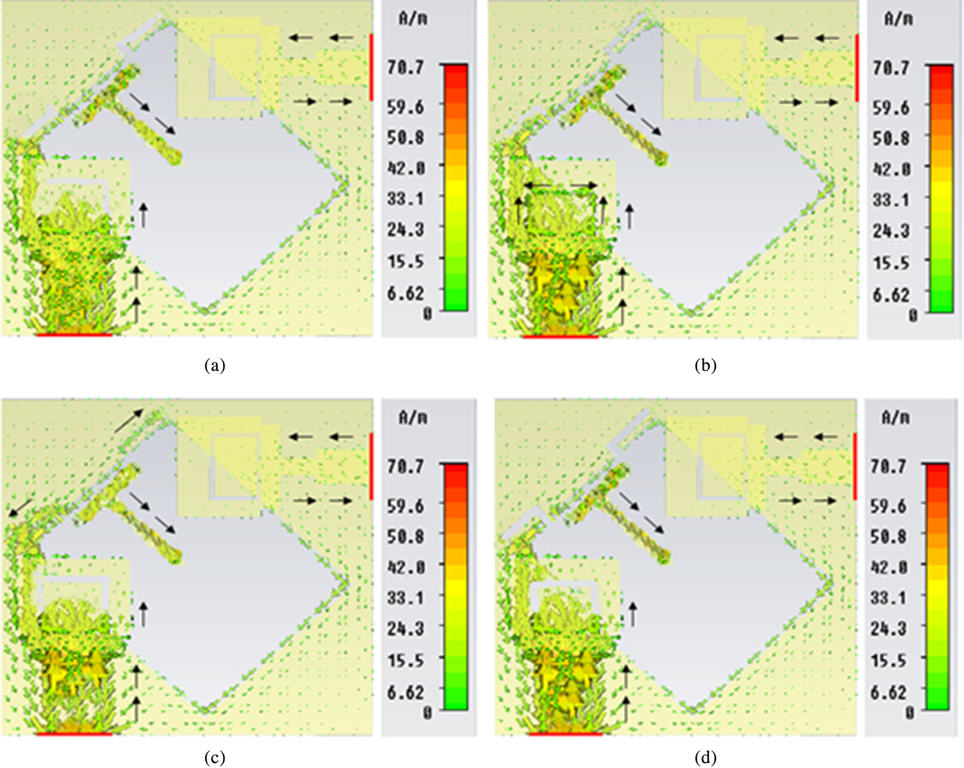
Fig. 15. Surface current distribution pattern of proposed antenna at: (a) 01.2 GHz, (b) 03.5 GHz, (c) 05.5 GHz, and (d) 19.4 GHz.
The diverse capability of a MIMO antenna can be determined with the help of “Envelope Correlation Coefficient” (ECC). Two methods are prevalent to compute the ECC. One is the method involving the “3D Radiation Pattern”. ECC can also be computed involving the “S-parameters”. The “3D Radiation Pattern” method is a bit complicated. So, the “S-parameter” method is commonly used due to its simplicity.
The ECC for Rayleigh Fading Channel (RFC) is expressed as,
 $$Q_e\, = \,\,\vert {Q_c} \vert ^2,$$
where Ϙ c is the “Complex-Correlation-Coefficient” [Reference Najam, Duroc and Tedjini16]. If multipath-environment is chosen for the operation of the system, ECC can be computed using the S-parameters as,
 $$Q_e = \displaystyle{{ \vert s_{\,jj}^{^\ast} s_{\,jk} + s_{kj}^{^\ast} s_{kk} \vert ^{\,2}} \over {\lpar {1- \vert s_{\,jj} \vert^{\,2}- \vert s_{kj} \vert^{\,2}} \rpar \;\lpar {1- \vert s_{kk} \vert^{\,2}- \vert s_{\,jk} \vert^{\,2}} \rpar }},$$
where j = 1 and k = 2, respectively [Reference Najam, Duroc and Tedjini16]. As shown in Fig. 16, the value of ECC is below 0.25, which is chosen as the threshold value in this case. It may be observed that at the notched frequency bands this threshold value is violated.

Fig. 16. Envelope Correlation Coefficient (ECC) of proposed antenna (simulated and measured).
Time domain analysis is also an important aspect to judge the applicability of the MIMO antenna. The Group Delay factor, Ψ g can be expressed as,
 $$\Psi _g\, = \,-\,\displaystyle{{\Delta \gamma} \over {\Delta \delta}}, $$
where Δγ and Δδ are the phase deviation and frequency deviation of the signal transmitted [Reference Najam, Duroc and Tedjini16]. Signal distortion occurs due to variation in group delay. Antenna C and its replica are placed at some distance apart for group delay measurement. The group delay plot of the antenna proposed has been displayed in Fig. 17. It is somewhat constant with some ripples obeying a certain limit ≤0.25 ns except at the notched frequency points. Ripples arise due to the noise effect. Figure 18 displays the anechoic chamber up for the measurement of the antenna responses. The size of the chamber is 6.5 m × 5.5 m × 3.0 m consisting of pyramid type urethane foam radio wave absorbers. Typically, frequencies ranging from 1 to 20 GHz can be measured. The shielding effectiveness is 50 dB (min) at 1.0 GHz and 40 dB (min) from 2 to 20 GHz. The results may be at times good for some frequencies, whereas for some frequencies the results may turn worse. It may happen due to reflection from the walls or due to some problems in the transmitting antenna. In such cases, one may try to bring the source and test antennas closer for achieving accurate results.

Fig. 17. Group delay of proposed antenna (simulated and measured).
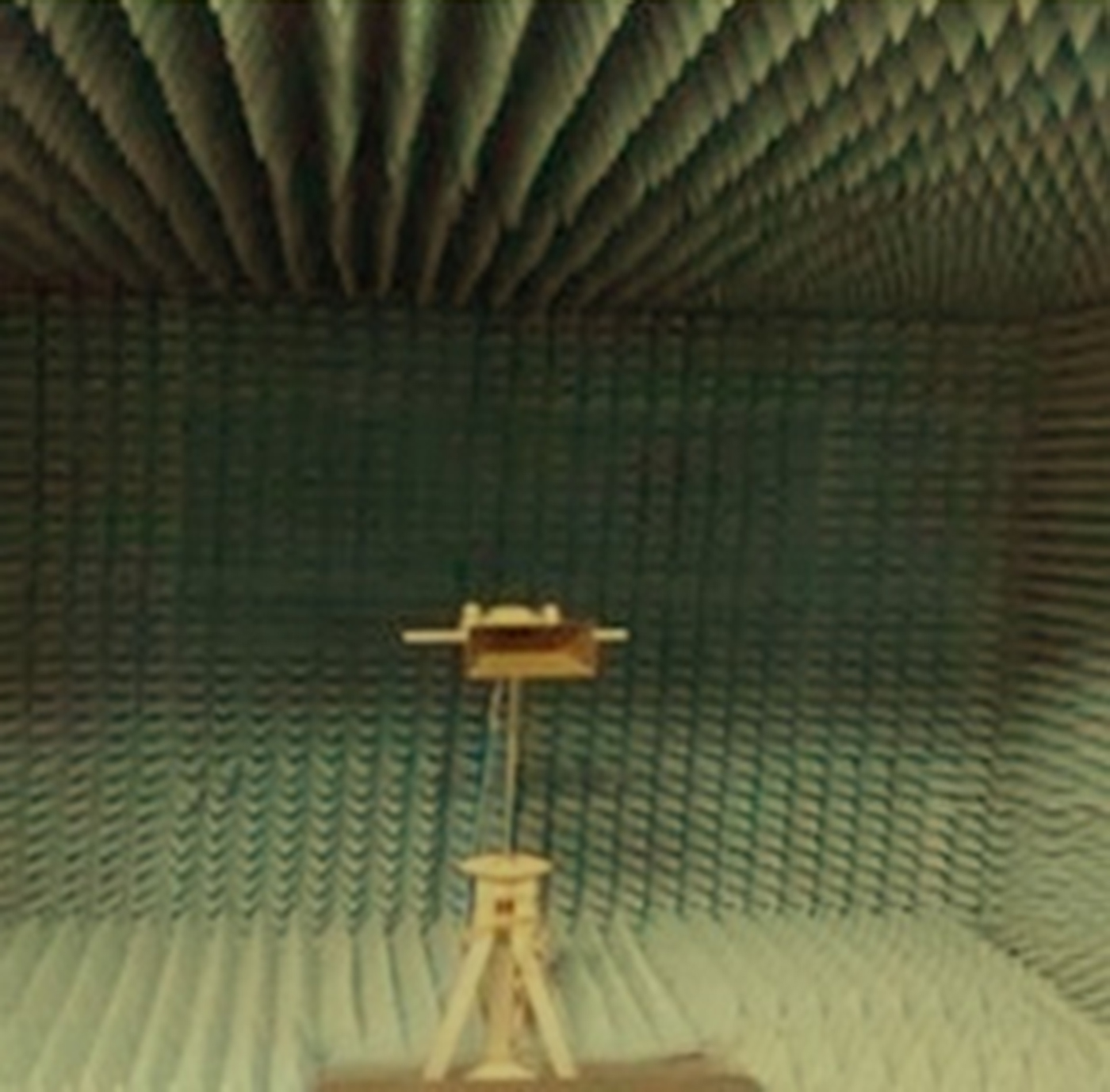
Fig. 18. Anechoic chamber for antenna measurement (Department of ETCE, Jadavpur University, Kolkata).
Conclusion
The antenna proposed here has a compact dimension of 20 mm × 20 mm. An extremely wide impedance bandwidth of 18.2 GHz (1.2–19.4 GHz) is achieved along with orthogonal radiation patterns and decent gain levels. It is one of the tiniest UWB–MIMO antennas available till date. Band-notching structures are incorporated and finely tuned to realize two band notches for blocking the undesired interference arising from the WLAN frequency band (5.5 GHz) and the WiMAX frequency band (3.5 GHz). Isolation between ports is enhanced by the addition of a simple parasitic structure between antenna elements. Super compactness and extremely wide impedance bandwidth are the key features of the proposed antenna. Satisfying all necessary specifications, the MIMO diversity antenna is no-doubt an efficient contender for communications supporting an extremely wide impedance bandwidth.
Author ORCIDs
Ankan Bhattacharya, 0000-0003-2350-1687; Rafael F. S. Caldeirinha, 0000-0003-0297-7870.
Acknowledgement
Two personalities who deserve to be acknowledged are Dr. Santosh K. Chowdhury, retired Professor of Jadavpur University, Kolkata, and Dr. Pranab Paul of Microline India, Kolkata, for their precious advices and provision of facilities for fabrication and measurement.
 Mr. Ankan Bhattacharya obtained the B.Tech. and M.Tech. degrees in Electronics and Communication Engineering from West Bengal University of Technology in 2010 and 2012 respectively. He is a Ph.D. Research Scholar in the Department of Electronics and Communication Engineering at the National Institute of Technology, Durgapur, West Bengal, India. He is also associated with Mallabhum Institute of Technology, Bishnupur, India. He is a Life-Member of FOSET (Forum of Scientists, Engineers and Technologists), Member of IEEE (Institute of Electrical and Electronics Engineers), and Member of Applied Computational Electromagnetics Society (ACES). His area of research is design and development of compact slotted antennas for wireless applications. His research articles have been published in many national and international journals and conferences.
 Dr. Bappadittya Roy obtained the B.Tech. and M.Tech. degrees in Electronics and Communication Engineering from West Bengal University of Technology, West Bengal, India in 2008 and 2011, respectively. He received his Ph.D. degree in Electronics and Communication Engineering from the National Institute of Technology, Durgapur, West Bengal, India. He is associated with Madanapalle Institute of Technology and Science, Madanapalle, India as a Senior Asst. Prof. of Electronics and Communication Engineering Department. He is a member of IEEE (Institute of Electrical and Electronics Engineers). His research areas are microstrip antennas, fractal antennas and mobile communication. He has received many national and international travel grants and has traveled abroad for seminars, conferences, and workshops. He has published several articles in reputed journals and conferences.
 Prof. (Dr.) Rafael F. S. Caldeirinha was born in Leiria, Portugal, in 1974. He received the B.Eng. (Hons) degree in Electronic and Communication Engineering from the University of Glamorgan, UK, in 1997. In 2001, he was awarded a Ph.D. in Radiowave Propagation by the same University. He is currently Head of the Antennas & Propagation (A&P-Lr) research group at Instituto de Telecomunicações, Leiria, Portugal, and a Coordinator Professor in Mobile Communications at the School of Technology and Management (ESTG) of the Polytechnic Institute of Leiria (IPL), Portugal. Prof. Caldeirinha has authored or co-authored more than 90 papers in conferences and international journals, one book chapter, and four contributions to ITU-R Study Group which formed the basis of the ITU-R P.833-5 (2005) recommendation. He is a member of the editorial board of the International Journal of Communication Systems, IJCS (New York, Wiley), Program Chair of WINSYS International Conference between 2006 and 2012, Appointed Officer for Awards and Recognitions of the IEEE Portugal section in 2014, Chair of the IEEE Portugal Joint Chapter on Microwave Theory & Techniques – Antennas & Propagation – Electron Devices since 2016, and a Senior Member of IEEE and a Fellow Member of IET.
 Prof. (Dr.) Anup Kumar Bhattacharjee received his B.E. degree in Electronics and Telecommunication Engineering from B.E. College Shibpur (presently Indian Institute of Engineering Science and Technology, Shibpur), Howrah, India in 1983. He received the M.E. and Ph.D. degrees from Jadavpur University, Kolkata, India in 1985 and 1989, respectively. Presently he is associated with the National Institute of Technology, Durgapur, West Bengal, India as a Senior Professor of Electronics and Communication Engineering Department. His research areas are electronic devices and circuits, microwave devices, microstrip antennas, embedded systems, VLSI systems, mobile communications, satellite communications, etc. He has successfully supervised over 13 Ph.D. students and has published over 120 articles in national and international journals, magazines, and conferences.