


Introduction
With the upcoming deployment of 5G-and-beyond wireless communications technologies in the near future, for which higher data rates will be necessary to provide advanced services and functionalities to the final user (e.g. virtual reality, augmented reality, or holographic video calls among many others), new satellite communications networks are expected to play a fundamental role [Reference Pham, Fang, Ha, Piran, Le, Le, Hwang and Ding1, Reference Rappaport, Xing, Kanhere, Ju, Madanayake, Mandal, Alkhateeb and Trichopoulos2]. Indeed, they are intended to serve as key support to terrestrial networks in those scenarios in which they may become saturated, due to the highly demanding traffic and capacity requisites resulting from an ever-growing density of users. As such, several initiatives for the development of co-integrated 5G-and-beyond/satellite networks have been initiated worldwide (e.g. see Table I in [Reference Lin, Huang, de Cola, Wang, Wang, Guizani and Wang3]), where the European Union is playing a major role through different projects promoted by the European Space Agency. In this scenario, the launching of large constellations of lightweight satellite units that may assure ubiquitous coverage will be essential, as fairly attested by the recent “nano/pico-satellite” and “CubeSat” revolution and related markets [Reference Hossain, Mirza, Soh, Jamlos, Sheikh, Al-Hadi and Akkaraekthalin4, Reference Bouça, Matos, Cunha and Carvalho5]. On the other hand, due to the current saturation of the electromagnetic spectrum as a very scarce resource, it will be mandatory for these co-integrated 5G-and-beyond/satellite communications systems to operate in various non-contiguous regions of the radio spectrum in order to accommodate their high-data-rate necessities that may reach up to 100 Gb/s [Reference Petrov, Kürner and Hosako6].
As radio frequency (RF)-hardware-enabling technologies for these next-generation wireless systems, the development of compact-size/low-volume RF circuits with multi-band operation is concentrating large interest. In the case of passive filtering components, planar implementations are gaining more attention in satellite communications scenarios for applications where commonly involved high-RF-power-handling requisites can be alleviated as in receiver RF front-ends. They also offer benefits in terms of easier integration with other RF components, such as amplifiers. Hence, a variety of research studies about microwave planar filtering devices aimed at satellite communications systems have been already reported, such as those in [Reference Llorente-Romano, García-Lampérez, Salazar-Palma, Daganzo-Eusebio, Galaz-Villasante and Padilla-Cruz7–Reference Gómez-García, Muñoz-Ferreras, Jiménez-Campillo, Branca-Roncati and Martín-Iglesias9]. They have addressed different research topics, such as the design of co-integrated planar-filter/3-dB-hybrid networks for Ku-band input multiplexers, the engineering of lossy intermediate-frequency (IF) planar filters with ultra-wide stopband, or the conception of passband-flattened/bandwidth-electronically reconfigurable IF planar filters that may allow us to replace more conventional and bulkier switchable-filter-bank-based RF pre-selectors.
Regarding multi-band multiplexers that may be exploited as multi-frequency channelizers in future satellite communications scenarios with multi-band-operation capabilities, much less research efforts have been made when compared to their single-band counterparts for which the technical literature is very wide [Reference Carceller, Soto, Boria, Guglielmi and Gil10–Reference Gómez-García, Yang, Muñoz-Ferreras and Psychogiou15]. For example, in [Reference Liu, Zhu, Wen, Zhang, Sun and Xu16], a super-conducting quad-band diplexer with dual-band channels using spiral-stub-loaded resonators was reported. Although it features remarkable performance in terms of in-band insertion loss for such narrow-band passbands as a benefit of the super-conductor technology, its suitability for frequency-contiguous-channel designs is not addressed. This is also the case of the six-band multi-path-stepped impedance resonator-based microstrip diplexer with three-band channels described in [Reference Chen, Wu, Dai and Su17] and the octo-band-stepped impedance resonator-based microstrip diplexer with four-band channels presented in [Reference Tu and Hung18], whose channelizing transfer functions are not spectrally allocated in a fully adjacent way. Therefore, there is a lack of multi-band planar diplexers allowing a flexible positioning of their channelizing filters including frequency-contiguous designs, while also featuring sharp-rejection filtering capabilities through multi-transmission zero generation.
In this study, a type of planar multi-band diplexer with sub-sets of spectrally imbricated passbands is reported. Their channelizing bandpass filters exploit a class of multi-resonant filtering stage with multi-passband/multi-notched-band sub-cells. Moreover, although particularized here in an octo-band microstrip diplexer, this concept can be extended to multiplexer designs with an arbitrary number of channels and passbands per channel and to different RF technologies.
The organization of the rest of the paper is as follows. In Section “Theoretical foundations,” the theoretical foundations and RF-operational principles of the devised approach of a multi-band diplexer with sub-sets of spectrally imbricated passbands are detailed by using a coupling–routing–diagram formalism. Here, the generation of additional transmission zeros by means of cross-coupling techniques is also proposed and exemplified. In Section “Experimental results,” a microstrip proof-of-concept prototype of an octo-band diplexer with pairs of frequency-contiguous passbands allocated within the 1.5–2.5 GHz band is manufactured and characterized for experimental-demonstration purposes, and properly compared with main state-of-the-art diplexer developments. Finally, a summary and the most-relevant concluding remarks of this study are provided in Section “Conclusion.”
Theoretical foundations
Operational principle
The normalized coupling–routing–diagram and conceptual operational principle of the proposed architecture of a multi-band diplexer with sub-sets of frequency-contiguous transmission bands is detailed in Fig. 1. Note that, for the sake of simplicity of the theoretical explanations provided below, the particular case of an octo-band diplexer with four-band channelizing bandpass filters is considered in this study. Nevertheless, this channelizer approach can be directly generalized to diplexer implementations featuring a higher number of transmission bands per channel, as well as to multiplexer realizations with more than two channels. As shown in Fig. 1, each channelizing bandpass filter consists of the in-series cascade connection of various replicas of a constituent multi-resonant filtering stage composed of two different sub-cells, as follows:
• A dual-passband sub-cell that creates the two main transmission bands – centered at the normalized frequencies $\Omega _1^{l}$
 and $\Omega _2^{l}$ $( \Omega _1^{l}< \Omega _2^{l})$ for the lower channel and $\Omega _1^{u}$ and $\Omega _2^{u}$ $( \Omega _1^{u}< \Omega _2^{u})$ for the upper channel – in the filtering transfer function of each channel.
• A dual-stopband sub-cell that produces two notched bands – centered at the normalized frequencies $\Omega _{n1}^{l}$
and $\Omega _{n2}^{l}$ $( \Omega _{n1}^{l}< \Omega _{n2}^{l})$ for the lower channel and $\Omega _{n1}^{u}$ and $\Omega _{n2}^{u}$ $( \Omega _{n1}^{u}< \Omega _{n2}^{u})$ for the upper channel as transmission-zero frequencies –, so that each of them splits each of the two main previously referred transmission bands into two sub-passbands.


Fig. 1. Multi-band diplexer concept with sub-sets of frequency-contiguous passbands (particular case of octo-band diplexer made up of two K-stage channelizing quadruple-band bandpass filters whose passbands are imbricated by pairs). (a) Normalized coupling–routing–diagram [black circles: resonating nodes; gray circles: zero-susceptance non-resonating nodes (NRNs); white circles: unitary source (S) and loads of the lower (Ll) and upper (Lu) channels; continuous lines: couplings; Y 0 = 1/Z 0: reference admittance for normalization; J variables: normalized admittance inverter constants; Ω (in rad/s): normalized frequency; $\Omega _1^{l},\; \, \Omega _2^{l}$ and $\Omega _1^{u},\; \, \Omega _2^{u}$
 : normalized resonant frequencies of the dual-passband sub-cells in lower and upper channels; $\Omega _{n1}^{l},\; \, \Omega _{n2}^{l}$
 and $\Omega _{n1}^{u},\; \, \Omega _{n2}^{u}$
 : normalized resonant frequencies of the dual-stopband sub-cells – i.e. transmission zeros – in lower and upper channels]. (b) Conceptual operational principle.
In this manner, by means of the splitting phenomenon of the transmission bands of the dual-passband sub-cell through the dual-stopband sub-cell, a quad-band filtering response per channel is generated. Furthermore, as illustrated in Fig. 1(b) and despite this technique is general for other situations, the sub-sets of split sub-passbands corresponding to the lower and upper channels can be spectrally imbricated for multi-band contiguous channel diplexer designs. Note that in the case that one single resonating node is used in the multi-passband sub-cell – i.e. single-passband sub-cell – or if the overall passbands before splitting that are centered at $\Omega _1^{u}$ and $\Omega _2^{l}$
 are designed to be frequency contiguous, a multi-band diplexer in which all the sub-passbands after splitting become spectrally adjacent – i.e. not only by sub-sets – can also be realized.
For theoretical demonstration purposes, examples of synthesized octo-band diplexers with first-, second-, and third-order channels (i.e. K = 1, 2, and 3) by means of the normalized coupling–routing–diagram detailed in Fig. 1 are presented in Fig. 2. These synthesis examples were derived through fine numerical optimization with Matlab of the normalized admittance inverter constants – all the values for the design variables are listed in Table 1 – aimed at maximizing the in-band power-matching levels for the four bands of both channels while satisfying a prefixed attenuation mask. It must be remarked upon that a closed analytical synthesis procedure for this type of multi-band diplexer, which relies on multi-extracted-pole techniques, is not available at this moment and its derivation remains as further research study. As expected, higher filtering selectivity levels are obtained in Fig. 2 as the number of stages per channel is increased. Specifically, the sub-passbands of each channel are spectrally imbricated in sub-sets of two for all the examples, showing transmission zeros between them as created by the dual-stopband sub-cells – between the first and the second sub-passbands and the third and the fourth sub-passbands – and the dual-passband sub-cell – between the second and the third sub-passbands. Note also that, whereas reflection zeros are attained for each sub-passband in the first-order example, minimum in-band power-matching levels of 14.3 and 11.6 dB are obtained for the second- and third-order cases, respectively.

Fig. 2. Theoretically synthesized power transmission (|S 21| and |S 31|) and input-reflection (|S 11|) responses of the octo-band diplexer concept for different number of stages K in the constituent quadruple-band bandpass filters (values for the design parameters listed in Table 1). (a) K = 1. (b) K = 2. (c) K = 3.

$\Omega _1^{l} = -\Omega _2^{l} = -5,\;$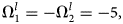 $\Omega _{n1}^{l} = -\Omega _{n2}^{l} = -5.5,\;$
$\Omega _1^{u} = -\Omega _2^{u} = -2.8,\;$ and $\Omega _{n1}^{u} = -\Omega _{n2}^{u} = -3.6$
 in all the examples.
Finally, it should be remarked upon that despite all the theoretical design examples provided in Fig. 2 exhibit narrower bandwidths for those transmission sub-bands that are closer to the overall normalized center frequency Ω = 0, the engineered multi-band diplexer concept is valid to fulfill a general set of specifications. For illustration purposes, Fig. 3 presents the theoretical power transmission and reflection responses of an example with broader bandwidths for those sub-passbands that are nearer to Ω = 0, which was simply derived from the example in Fig. 2(b) by making $\Omega _{n1}^{l} = -\Omega _{n2}^{l} = -8.5$ and $\Omega _{n1}^{u} = -\Omega _{n2}^{u} = -6.6$
 (the rest of the design variables remain with the same values as those listed in Table 1 for the example in Fig. 2(b)). In this case, minimum in-band power-matching levels of 13 dB are obtained for all the sub-passbands – which are located at non-contiguous spectral positions in this particular example –, thus revealing the generality of this multi-band diplexer principle.

Fig. 3. Example of theoretically synthesized power transmission (|S 21| and |S 31|) and input-reflection (|S 11|) responses of the second-order octo-band diplexer concept (i.e. K = 2) in which the bandwidths of those sub-passbands that are closer to Ω = 0 are spectrally wider than the other sub-passbands ($\Omega _{n1}^{l} = -\Omega _{n2}^{l} = -8.5$ , $\Omega _{n1}^{u} = -\Omega _{n2}^{u} = -6.6$
 , and the rest of the design variables remain the same as listed in Table 1 for the design example in Fig. 2(b)).
Sharper-rejection designs through cross-coupling techniques
Although the theoretically synthesized diplexer examples provided in Figs 2 and 3 exhibit filtering transfer functions for both channels with a transmission zero between each pair of sub-passbands, adjacent transmission zeros below and above the first and fourth sub-passbands are not created. To counteract this limitation, the multi-band diplexer architecture presented in Fig. 1 can be modified to create additional transmission zeros by exploiting cross-coupling techniques. Although different cross-coupling solutions may be adopted, a suitable choice is the incorporation of such cross coupling between the NRNs of the dual-passband sub-cells of adjacent multi-resonant stages at each channel. This is illustrated in Fig. 4 for a second-order octo-band diplexer architecture (i.e. K = 2), in which the additional “opposite-sign weak” coupling path between the two multi-resonant stages in both channels allows the creation of extra transmission nulls. To verify this technique, a theoretically synthesized diplexer example associated to the normalized coupling–routing–diagram in Fig. 4 is provided in Fig. 5 – all the values for the design variables are listed in Table 1. As can be seen, additional transmission zeros below and above the first and fourth sub-passbands, respectively, as well as in-between the second and third sub-passbands, are produced while maintaining a minimum in-band power-matching level of 13.9 dB. As such, sharper-rejection filtering capabilities are achieved in this case when compared to the one without cross-coupling.

Fig. 4. Normalized coupling–routing–diagram of an octo-band diplexer with additional transmission-zero generation through cross coupling (dashed lines: cross couplings).

Fig. 5. Theoretically synthesized power transmission (|S 21| and |S 31|) and input-reflection (|S 11|) responses of the octo-band diplexer concept for second-order quadruple-band bandpass filters with cross coupling (values for the design parameters listed in Table 1).
In a fully transmission-line design, the cross-coupling path between adjacent multi-resonant filtering stages can be realized by means of an inductive-type interaction. Specifically, it can be implemented by using a high-impedance transmission-line section that connects the involved zero-susceptance NRNs of the contiguous multi-resonant filtering stages. Note that the electrical length of this inductive-type/high-impedance transmission-line segment needs to be properly adjusted, since it directly affects the locations of these transmission zeros. For demonstration purposes, Fig. 6(a) shows the transmission-line circuit scheme of a diplexer channel (quadruple-band bandpass channel as in the example of Fig. 5), in which the inductive-type transmission-line segment between its two constituent multi-resonant filtering stages has been introduced. For a more-compact realization, the impedance inverters that are adjacent to the resonating lines in the dual-passband sub-cells have been absorbed. Figure 6(b) presents the theoretical power transmission and reflection responses for this circuit, which are compared with its diplexer counterpart without the extra transmission zeros (i.e. by omitting the inductive-type transmission-line segment). As observed, the creation of the extra transmission nulls with the inductive-type transmission line in this distributed element design is verified.
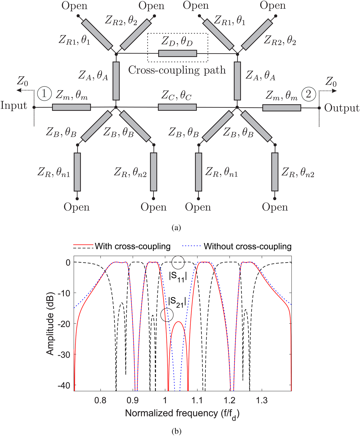
Fig. 6. Example of quadruple-passband channelizing filter with cross-coupling for additional transmission-zero generation. (a) Transmission-line realization (Z and θ variables refer to characteristic-impedance and electrical-length parameters of a transmission line, respectively, and Z 0 is the reference/port impedance). (b) In-band details of the power transmission (|S 21|) and input-reflection (|S 11|) responses (Z m = 1.5Z 0, Z A = 0.6Z 0, Z B = 2.4Z 0, Z C = 1.8Z 0, Z D = 2.8Z 0, Z R1 = 0.4Z 0, Z R2 = Z R = 0.6Z 0, $\theta _1( f_d) = 60o$ , $\theta _2( f_d) = 105o$
 , $\theta _{n1}( f_d) = 145o$
 , $\theta _{n2}( f_d) = 200o$
 , $\theta _A( f_d) = \theta _B( f_d) = \theta _C( f_d) = \theta _m( f_d) = 90o$
 , and $\theta _D( f_d) = 260o$
 where f d is the design frequency).
Moreover, as a further application, note that such cross-coupling path may also be exploited to produce an in-band notch over a wider-band passband of the multi-band filtering response of a single channelizing filter (i.e. the extra upper transmission zero can be embedded within the wide upper passband). This is demonstrated in Fig. 7 through a supportive design example of a triple-band bandpass channelizing filter with an in-band notch that is inserted within the upper transmission band.

Fig. 7. Example of quadruple-passband channelizing filter with cross-coupling for additional transmission-zero generation. (a) Transmission-line realization (Z and θ variables refer to characteristic-impedance and electrical-length parameters of a transmission line, respectively, and Z 0 is the reference/port impedance). (b) In-band details of the power transmission (|S 21|) and reflection (|S 11|) responses (Z m = 1.5Z 0, Z A = 0.8Z 0, Z B = 2.4Z 0, Z C = 1.7Z 0, Z D = 2.6Z 0, Z R1 = 0.4Z 0, Z R2 = Z R = 0.6Z 0, $\theta _1( f_d) = 60o$ , $\theta _2( f_d) = 105o$
 , $\theta _{n}( f_d) = 200o$
 , $\theta _A( f_d) = \theta _B( f_d) = \theta _C( f_d) = \theta _m( f_d) = 90o$
 , and $\theta _D( f_d) = 310o$
 where f d is the design frequency).
Experimental results
To demonstrate the practical usefulness of the engineered concept of the multi-band planar diplexer with sub-sets of spectrally adjacent passbands, a proof-of-concept second-order prototype has been developed using microstrip technology and characterized. Specifically, it was designed to operate within the frequency range of 1.5–2.5 GHz and to feature four transmission bands for each channelizing filter – i.e. octo-band diplexer – that are imbricated in sub-sets of two. Starting from its corresponding coupling–routing–diagram representation as illustrated in Section “Theoretical foundations,” the diplexer was implemented in a fully transmission-line arrangement after applying conventional microwave filter design techniques that involve frequency transformation and admittance-scaling processes [Reference Hunter19, Reference Hong20]. As such, the resonating nodes were realized as open-ended half-wavelength transmission-line resonators at their respective natural frequencies and the admittance inverters as quarter-wavelength transmission-line sections. Owing to the frequency dependency of these transmission-line-based admittance inverters that is not contemplated by the coupling–routing–diagram formalism, as well as to the different frequency-variation profile of the transmission-line resonators with regard to the ideal ones, a fine optimization of the overall circuit was needed to maximize the in-band input-power-matching levels for all the transmission bands.
The layout and a photograph of the built microstrip prototype of the octo-band diplexer are shown in Fig. 8. The main parameters of the employed microstrip substrate and its geometrical variables – as marked in Fig. 8(a) – are as follows:

Fig. 8. Manufactured microstrip prototype of the octo-band diplexer. (a) Layout. (b) Photograph.
• 4003C microstrip substrate: relative dielectric permittivity ɛr = 3.38, dielectric thickness H = 1.524 mm, metal thickness t = 35μm, and dielectric loss tangent tan(δD) = 0.0027.
• Inner lengths (l), widths (w), and inter-adjacent-line spacings (s) in mm (cross- and T-type junctions are not considered): w a = 3.38, l a = 87, w x = 3.88, l x = 10, $w_{b_1} = 1.9,\;$
$l_{b_1} = 19.5,\;$ $w_{c_1} = 0.9,\;$ $l_{c_1} = 17.4,\;$ $w_{d_1} = 1.9,\;$ $l_{d_1} = 20.5,\;$ $w_{e_1} = 3.38,\;$ $l_{e_1} = 21,\;$ $w_{f_1} = 9.52,\;$ $l_{f_1} = 28.3,\;$ $w_{g_1} = 9.52,\;$ $l_{g_1} = 28.3,\;$ $w_{h_1} = 1.22,\;$ $l_{h_1} = 28.2,\;$ $w_{k_1} = 1.22,\;$ $l_{k_1} = 30.4,\;$ $s_{h_1k_1} = 0.56,\;$ $w_{l_1} = 1.22,\;$ $l_{l_1} = 30.8,\;$ $w_{m_1} = 1.22,\;$ $l_{m_1} = 27.3,\;$ $s_{l_1m_1} = 0.56,\;$ $w_{p_1} = 9.03,\;$ $l_{p_1} = 16.2,\;$ $w_{q_1} = 9.52,\;$ $l_{q_1} = 30.1,\;$ $w_{r_1} = 9.03,\;$ $l_{r_1} = 16.2,\;$ $w_{s_1} = 9.52,\;$ $l_{s_1} = 30.1,\;$ $w_{t_1} = 7.11,\;$ $l_{t_1} = 64.4,\;$ $w_{u_1} = 11.96,\;$ $l_{u_1} = 42.5,\;$ $s_{t_1u_1} = 2.82,\;$ $w_{v_1} = 11.96,\;$ $l_{v_1} = 42.5,\;$ $w_{w_1} = 7.11,\;$ $l_{w_1} = 64.3,\;$ $s_{v_1w_1} = 2.82,\;$ $w_{b_2} = 1.9,\;$ $l_{b_2} = 17.9,\;$ $w_{c_2} = 0.9,\;$ $l_{c_2} = 18.6,\;$ $w_{d_1} = 1.9,\;$ $l_{d_1} = 22.8,\;$ $w_{e_2} = 3.38,\;$ $l_{e_2} = 14,\;$ $w_{f_2} = 9.52,\;$ $l_{f_2} = 24.3,\;$ $w_{g_2} = 9.52,\;$ $l_{g_2} = 24.3,\;$ $w_{h_2} = 1.22,\;$ $l_{h_2} = 25.1,\;$ $w_{k_2} = 1.22,\;$ $l_{k_2} = 30.7,\;$ $s_{h_2k_2} = 0.56,\;$ $w_{l_2} = 1.22,\;$ $l_{l_2} = 31,\;$ $w_{m_2} = 1.22,\;$ $l_{m_2} = 24.3,\;$ $s_{l_2m_2} = 0.56,\;$ $w_{p_2} = 9.03,\;$ $l_{p_2} = 16.8,\;$ $w_{q_2} = 9.52,\;$ $l_{q_2} = 27.2,\;$ $w_{r_2} = 9.52,\;$ $l_{r_2} = 27.2,\;$ $w_{s_2} = 9.03,\;$ $l_{s_2} = 16.8,\;$ $w_{t_2} = 7.11,\;$ $l_{t_2} = 59.1,\;$ $w_{u_2} = 11.96,\;$ $l_{u_2} = 39.5,\;$ $s_{t_2u_2} = 1.84,\;$ $w_{v_2} = 11.96,\;$ $l_{v_2} = 39.5,\;$ $w_{w_2} = 7.11,\;$ $l_{w_2} = 55.5,\;$ and $s_{v_2w_2} = 1.84.$


Note that, if needed by the intended application, higher size compactness may be attained by using meandered lines for the high-impedance transmission-line impedance inverters and/or capacitively loaded transmission-line resonators [Reference Ghali and Moshely21, Reference Jarry and Beneat22]. Moreover, for designs aimed at the lower part of the microwave region where insertion loss becomes less critical, lumped/quasi-lumped-element implementations may also be considered to achieve further physical-size reduction [Reference Loeches-Sánchez, Psychogiou, Gómez-García and Peroulis23].
The simulated (with the electromagnetic software package Ansys HFSS) and measured (with a Keysight 5224A network analyzer) power transmission, input-reflection, and in-band group-delay responses for each channel of the manufactured microstrip circuit of the octo-band diplexer are compared in Fig. 9. As it can be seen, a fairly close agreement between simulated and measured results is obtained, hence fully verifying the proposed principle of RF multi-band diplexer with sub-sets of frequency-contiguous passbands. The main measured performance metrics for this diplexer circuit are as follows:
• Lower channel from its first to fourth passbands: center frequencies of 1.3, 1.52, 1.81, and 1.98 GHz, 3-dB absolute bandwidths equal to 86, 109, 62, and 79 MHz – i.e. equal to 6.6, 7.2, 3.4, and 4% in relative terms –, minimum in-band power-insertion-loss levels of 1.1, 1, 2.3, and 1.8 dB, in-band power-matching levels equal to 19.6, 12.8, 12.1, and 12.8 dB, maximum in-band group-delay variations of 10.4, 7.6, 7.8, and 2.9 ns, and inter-band transmission zeros at 1.38, 1.68, and 1.88 GHz, respectively.
• Upper channel from its first-to-fourth passbands: center frequencies equal to 1.4, 1.64, 1.88, and 2.08 GHz, 3-dB absolute bandwidths of 86, 102, 73, and 93 MHz – i.e. equal to 6.1, 6.7, 3.9, and 4.5% in relative terms –, in-band power-insertion-loss levels lower than 1.2, 1.3, 2.2, and 2.3 dB, in-band power-matching levels of 19.9, 11.8, 10.3, and 12.6 dB, maximum in-band group-delay variations equal to 9.4, 5.5, 5.8, and 7.7 ns, and inter-band transmission zeros at 1.49, 1.79, and 1.99 GHz, respectively.

Fig. 9. Simulated and measured power transmission (|S 21| and |S 31|), reflection (|S 11|), and group-delay ($\tau _g^{21}$ and $\tau _g^{31}$
 ) responses of the manufactured microstrip prototype of the octo-band diplexer. (a) |S 21|, |S 31|, and |S 11|. (b) $\tau _g^{21}$
 . (c) $\tau _g^{31}$
 .
.
Note that the measured values for the maximum in-band group-delay variations for the different sub-passbands of this octo-band diplexer prototype correspond to average in-band phase-distortion metrics, since no self-equalization procedures – whose application remains as further research study to be addressed – were applied to this particular design.
Finally, a performance comparison of the multi-band diplexer prototype developed in this study with other exponents of prior-art single-/multi-band diplexer realizations using various technologies and resonator configurations is provided in Table 2. As it can be seen, among all the diplexer circuits with frequency-contiguous channels – either all their transmission bands or by sub-sets in the case of multi-band diplexers –, the one of this study features the highest number of passbands and transmission zeros per channel, along with full spectral imbrication of sub-sets of transmission bands.
Table 2. Comparison with other prior-art diplexers

TZs: transmission zeros; FBWs: fractional bandwidths.
Conclusion
An original type of multi-band planar diplexer with sub-sets of imbricated transmission bands and its coupling–routing–diagram formalism has been presented. Its usefulness to develop high-frequency multi-band diplexers, even including additional transmission zeros for sharper-rejection realizations by exploiting cross-coupling procedures, has been demonstrated at the theoretical design level through various illustrative examples. Furthermore, the practical viability of this diplexer concept has been verified through the development and testing of a microstrip prototype of a 1.5–2.5-GHz range octo-band diplexer shaped by two quad-band channelizing filters with pairs of frequency-contiguous passbands. Finally, note that the devised multi-band diplexer scheme can be scaled to channelizing circuits with more than two channels – e.g. triplexer or quadruplexer – and other technologies, such as 3-D/waveguide and substrate-integrated waveguide ones.
Acknowledgement
This study was supported in part by the Spanish Ministry of Economy, Industry, and Competitiveness (State Research Agency) under Project TEC2017-82398-R, in part by the GOT ENERGY TALENT (GET) fellowship program co-funded by the EU as part of the H2020-MSCA-COFUND program (Grant Agreement number 754382), and in part by the National Science Foundation under Grant ECCS-1731956.
 Roberto Gómez-García received his Dipl.-Eng. degree in telecommunication engineering and his Ph.D. degree in electrical and electronic engineering from the Polytechnic University of Madrid, Madrid, in 2001 and 2006, respectively. Since 2006, he has been an Associate Professor with the Department of Signal Theory and Communications, University of Alcalá, Alcalá de Henares, Spain. He has been, for several research stays, with the C2S2 Department, XLIM Research Institute, University of Limoges, Limoges, France, the Telecommunications Institute, University of Aveiro, Aveiro, Portugal, the U.S. Naval Research Laboratory, Microwave Technology Branch, Washington, DC, USA, and Purdue University, West Lafayette, IN, USA. He is also an Adjunct Part-Time Professor with the University of Electronic Science and Technology of China, Chengdu, China, as has been an Invited Professor with the Gdansk University of Technology, Poland, during 2019–2020. His current research interests include the design of fixed/tunable high-frequency filters and multiplexers in planar, hybrid, and monolithic microwave-integrated circuit technologies, multifunction circuits and systems, and software-defined radio and radar architectures for telecommunications, remote sensing, and biomedical applications. In these topics, he has authored/co-authored about 115 papers in international journals and 150 papers in international conferences.
Dr. Gómez-García serves as a member for the Technical Review Board for several IEEE and EuMA conferences. He is also a member of the IEEE MTT-S Filters (MTT-5), the IEEE MTT-S RF MEMS and Microwave Acoustics (MTT-6), the IEEE MTT-S Wireless Communications (MTT-23), the IEEE MTT-S Biological Effects and Medical Applications of RF and Microwave (MTT-28), and the IEEE CAS-S Analog Signal Processing Technical Committees. He was a recipient of the 2016 IEEE Microwave Theory and Techniques Society (MTT-S) Outstanding Young Engineer Award. He is an IEEE CAS-S Distinguished Lecturer (2020–2022). He was an Associate Editor of the IEEE Transactions on Microwave Theory and Techniques from 2012 to 2016 and the IEEE Transactions on Circuits and Systems-I: Regular Papers from 2012 to 2015. He was a Senior Editor of the IEEE Journal on Emerging and Selected Topics in Circuits and Systems from 2016 to 2017. He was a Guest Editor for several Special/Focus Issues and Sections in IEEE and IET journals. He is currently an Associate Editor of the IEEE Microwave and Wireless Components Letters, IEEE Journal of Electromagnetics, RF and Microwaves in Medicine and Biology, IEEE Access, IET Microwaves, Antennas, and Propagation, and the International Journal of Microwave and Wireless Technologies, a TC-5 Topic Editor of IEEE Journal of Microwaves, and the MTT-S Newsletter Working Group Chair.
 Li Yang received his M.Sc. degree in electrical and electronics engineering and his Ph.D. degree in electrical and computer engineering from the University of Macau (UM), Macau, China, in 2013 and 2018, respectively. In 2018, he was a Research Associate with the Department of Electrical and Computer Engineering, UM. Since 2018, he holds a post-doctoral position with the Department of Signal Theory and Communications, University of Alcalá, Alcalá de Henares, Spain, where he is currently a GOT ENERGY TALENT (GET)-COFUND Marie Curie Fellow. His current research interests include the synthesis and design of RF/microwave planar and multilayered passive filters, reconfigurable filters, filtering antennas, and multifunctional circuits and systems. Dr. Yang was a recipient of the Best Student Paper Award of the International Symposium on Antennas and Propagation 2010 in Macau.
 José-María Muñoz-Ferreras received his Dipl.-Eng. degree in telecommunication engineering and his Ph.D. degree in electrical and electronic engineering from the Polytechnic University of Madrid, Spain, in 2004 and 2008, respectively. He is currently an Associate Professor with the Department of Signal Theory and Communications, University of Alcalá, Alcalá de Henares, Spain. His current research interests include radar signal processing, advanced radar systems and concepts, and microwave/RF circuits and systems, specifically focusing on high-resolution inverse synthetic aperture radar images, and the design and validation of radar systems for short-range applications. Dr. Muñoz-Ferreras is a member of the IEEE MTT-S Biological Effects and Medical Applications of RF and Microwave (MTT-10) Technical Committee and a reviewer for several IEEE and IET publications. He serves as a member of the Technical Review Board of the IEEE International Geoscience and Remote Sensing Symposium, the IEEE Radar Conference, the European Radar Conference, and the IEEE MTT-S International Microwave Symposium.
 Dimitra Psychogiou received her Dipl.Eng. degree in electrical and computer engineering from the University of Patras, Patras, Greece, in 2008, and her Ph.D. degree in electrical engineering from the Swiss Federal Institute of Technology (ETH), Zürich, Switzerland, in 2013. From 2013 to 2016, she was with Purdue University, West Lafayette, IN, USA. From 2016, she is an Assistant Professor of electrical, computer and energy engineering with the University of Colorado at Boulder (UC Boulder), Boulder, CO, USA. Her research has been presented in more than 160 IEEE publications. Her current research interests include RF design and characterization of reconfigurable microwave and millimeter-wave passive components, RF-MEMS, acoustic wave resonator-based filters, tunable filter synthesis, and frequency-agile antennas.
Dr. Psychogiou is a Senior Member of URSI and an elected member of the IEEE MTT-S Filters and Passive Components (MTT-5) Technical Committee and the IEEE MTT-S Microwave Control Materials and Devices (MTT-13) Committee, where she is currently serving as the Vice-Chair. She received the 2020 CAREER Award from the National Science Foundation (NSF), the 2020 URSI Young Scientist Award, and the Junior Faculty Outstanding Research Award from UC Boulder. She is also an Associate Editor of the IEEE Microwave and Wireless Components Letters and IET Microwaves, Antennas, and Propagation and serves on the Technical Review Board for various the IEEE and EuMA conferences and journals. She is also the Secretary of the USNC-URSI Commission D.


