


I. INTRODUCTION
Frequency multipliers based on Schottky diodes are very useful for atmosphere and space detection at millimeter-wave and submillimeter-wave frequency band [Reference Crowe, Bishop, Porterfield, Hesler and Weikle1, Reference Maestrini2]. These multipliers are usually designed with Schottky diodes or heterostructure barrier varactor diodes [Reference Vukusic3]. Balanced frequency multipliers are most popular for their simple idle circuits and high conversion efficiency. For example, the balanced frequency tripler traps the even harmonics in the circle of the diode pair, so lossy output filter is not needed [Reference Maestrini4]. Proper DC bias is important to achieve high conversion efficiency and broadband operation. The diodes are usually self-biased or biased with external DC bias. The traditional balanced frequency triplers usually adopt anti-parallel diodes without external DC bias [Reference Chen and Xu5], or use series diodes with DC bias applied from an on-chip bias capacitor [Reference Maestrini4, Reference Maestrini, Ward, Chattopadhyay, Schlecht and Mehdi6].
Recently, power-combined frequency multipliers are extensively studied to raise the output power to pump the following higher frequency multipliers or pump the multi-receiver array. Two-way waveguide power-combined multiplier [Reference Chen and Xu5–Reference Kirby, Li, Xiao, Hesler and Papapolymerou7] is the most popular scheme. Y-junction and waveguide branch-line coupler [Reference Kirby, Li, Xiao, Hesler and Papapolymerou7, Reference Maestrini8] are usually adopted to split the input signal as well as recombine the output signal before and after multiplication. Waveguide spatial power combining [Reference Deng, Jiang and Ning9] scheme combines several multiplier chips simultaneously inside one single waveguide. However, it is difficult to assemble more than two multiplier chips together in one waveguide channel.
A 2N-diode power-combined frequency tripler designed with coupled suspended substrate stripline (SSS) [Reference Fu, Lu, Kwok and Lee10] is proposed in this work. The tripler adopts 2N anti-parallel diodes, with N parallel diodes on the front side of SSS and the other N parallel diodes on the back side. The front and the back diodes are in anti-parallel connection. The front diodes are equivalent to a single diode when analyzing the frequency tripler theoretically, and so does the back diodes.
II. ANALYSIS OF COUPLED SSS
SSS possesses quality factor much higher than microstrip line, while maintains the high fabrication accuracy and low cost, benefitting from the printed circuit process. Thus, SSS has extensive applications in low loss passive and active integrated circuits, such as filter, diplexer and mixer. Transmission lines of SSS are printed on either side or both sides of the suspended substrate. In the latter case, SSS supports two transmission modes [Reference Siles11], named even mode and odd mode as shown in Fig. 1.
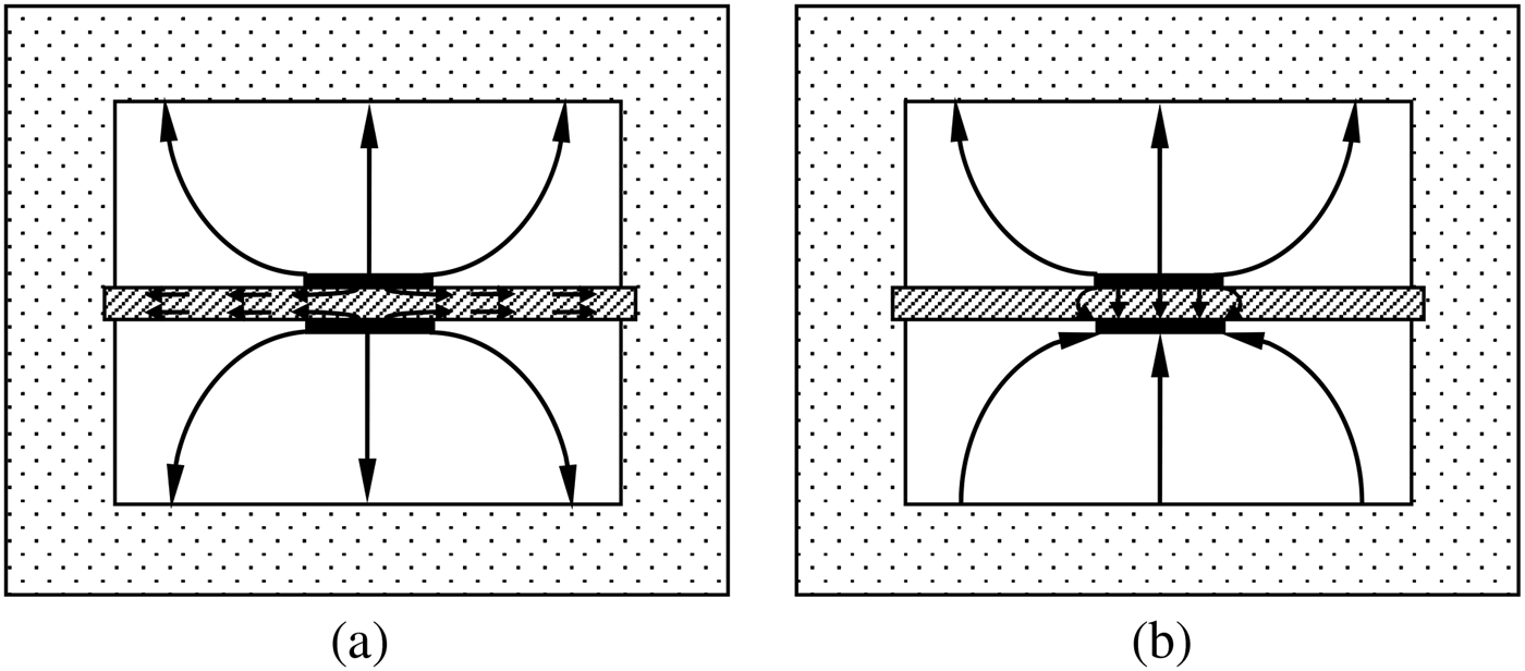
Fig. 1. Electric field distribution of coupled SSS. (a) Even mode; (b) odd mode.
For even mode, the electric field lines are symmetrical about the central plane along the substrate. If two identical circuits are printed on each side, the coupled SSS functions as in-phase power divider to divide the input power into two ways.
In order to achieve in-phase power combining, waveguide-to-SSS transition exciting only even mode needs be designed. Fortunately, the simple E-probe waveguide-to-SSS transition only excites even mode, while suppressing the odd mode. The model of the transition and its simulated results are shown in Fig. 2. The input port is WR-62 waveguide, port 2 is a two-mode output port, and port 3 is DC bias port. The input waveguide is a three-step reduced height waveguide to achieve broadband transition. A hammer-head low pass filter (LPF) [Reference Oswald and Siegel12] is used to reject the input signal from leaking to the bias port. As shown in Fig. 2, the excited odd mode signal at port 2 is at least 50 dB lower than the even mode. This waveguide-to-SSS transition is used to convert the exciting signal of the multiplier to coupled SSS mode.
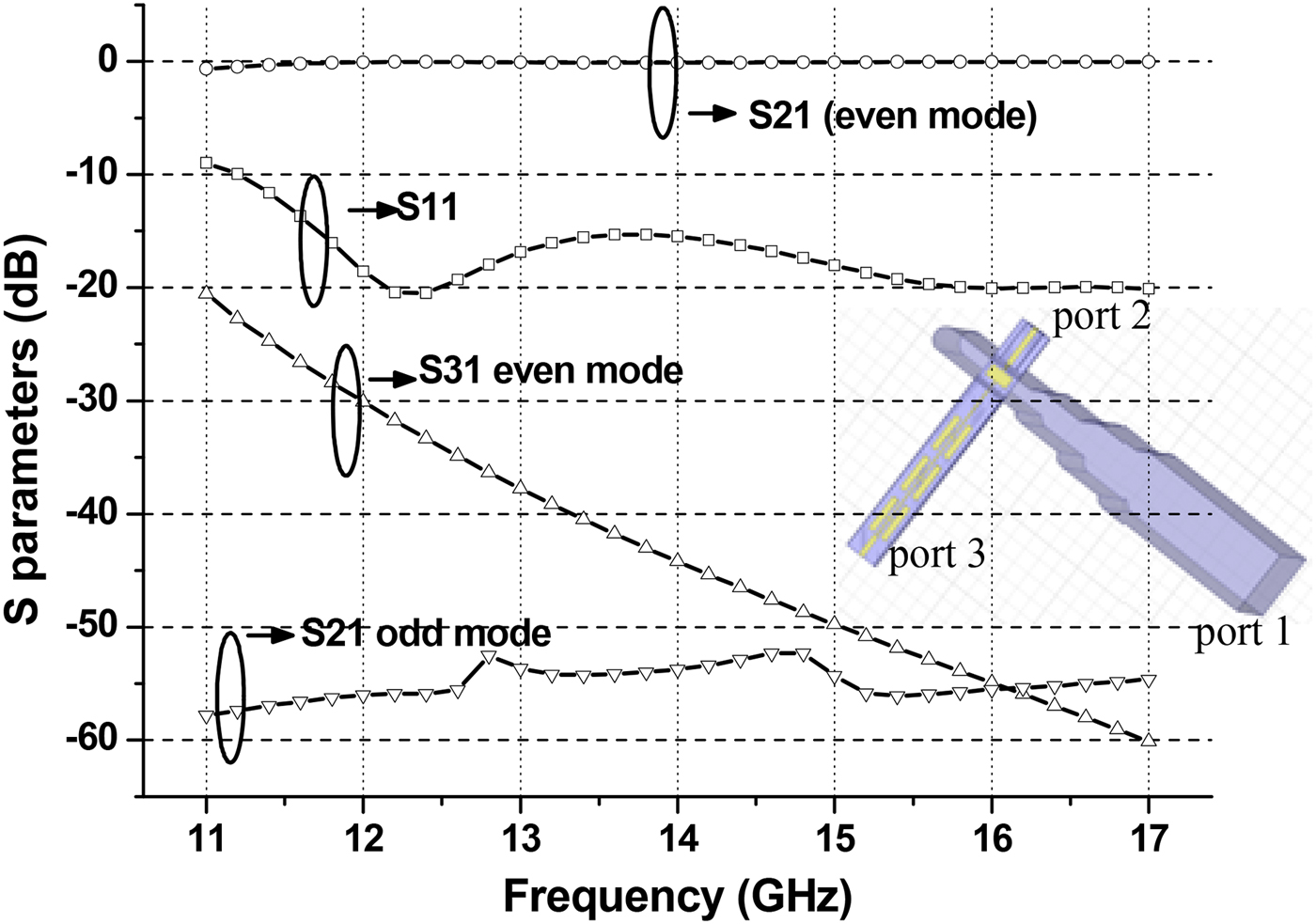
Fig. 2. E-probe waveguide to coupled SSS transition model and simulated results.
After the third harmonic of the multiplier is produced, another waveguide-to-SSS transition is also needed to convert the coupled SSS mode to waveguide mode. Recently, we have presented a grounded E-probe waveguide-to-SSS transition [Reference Guo, Xu, Cui, Xu and Qian13], which fits for this application.
The grounded probe not only converts the coupled SSS mode signal to waveguide mode, but also provides DC grounding for the Schottky diodes. The simulation model and results of the transition are shown in Fig. 3. The high impedance E-probe is matched to the coupled SSS with step impedance transformer. DC grounding is fulfilled by connecting the probes to the broad side of waveguide wall.
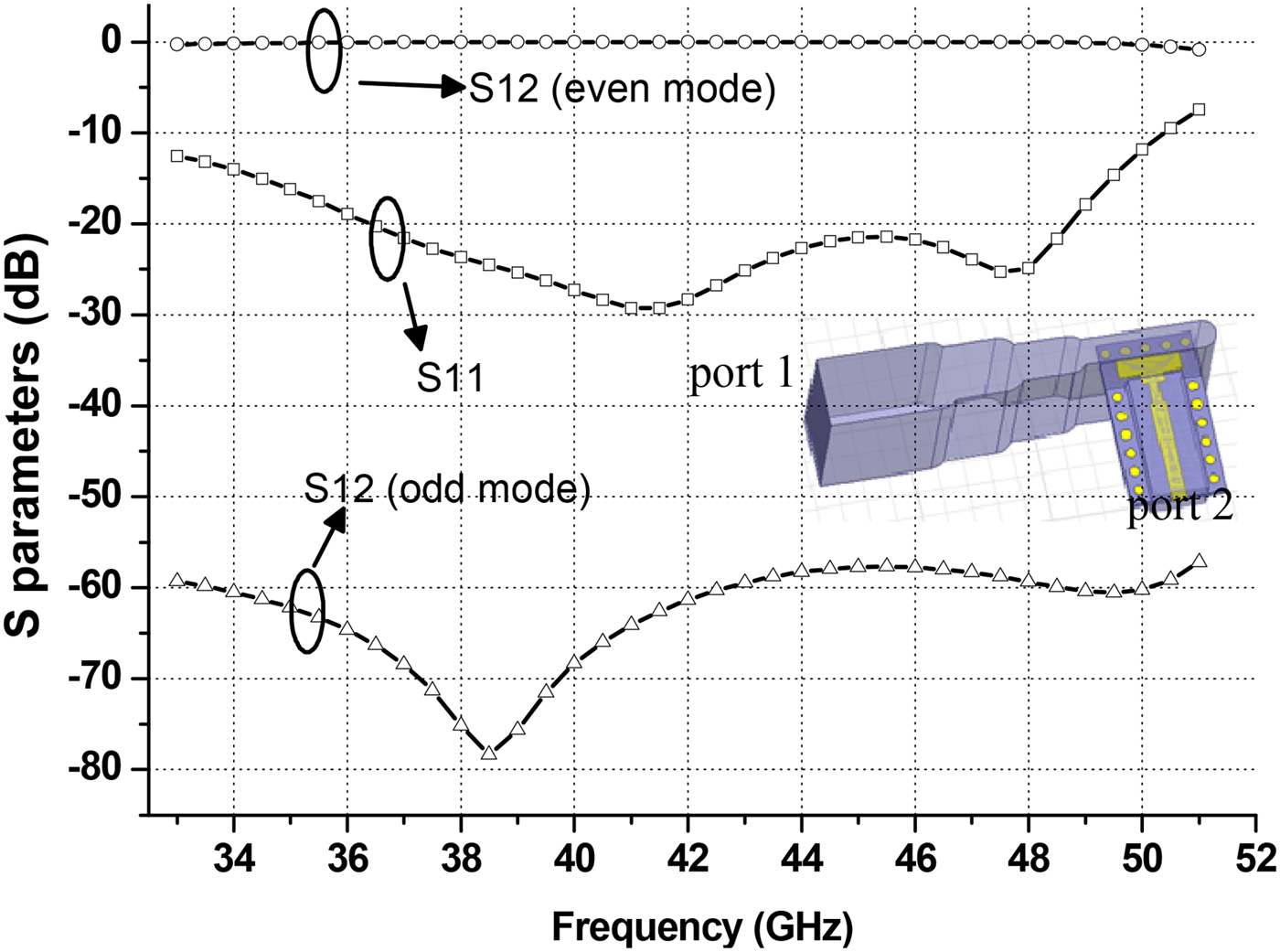
Fig. 3. Grounded E-probe waveguide to coupled SSS transition model and simulated results.
As shown in Fig. 3, the excited odd mode is at least 55 dB lower than the even mode at frequencies from 33 to 51 GHz.
Based on the analysis and simulated results above, both the input and the output waveguide-to-SSS transitions only excite even mode signal. The output transition also provides DC grounding for the diodes.
III. PROPOSED BALANCED FREQUENCY TRIPLER WITH TWO DIODES
The proposed balanced frequency tripler is illustrated in Fig. 4. The solid line represents the front circuit of the substrate, while the dashed line represents the back circuit. The input even mode signal is excited by the E-probe waveguide-to-SSS transition. An input LPF is used to reflect the third harmonic produced by the Schottky diodes, in case of which leaking to the input port. Input and output matching circuits are necessary if high conversion efficiency is expected. The output SSS-to-waveguide transition adopts grounded E-probe, which provides DC grounding for the Schottky diodes. This tripler needs at least two diodes with one diode on the front side and the other on the back side. As shown in Fig. 4, the front diode is mounted with anode connected to input matching circuit, and the back diode is mounted with cathode connected to input matching circuit. This way, two diodes can be biased separately. The bias voltage for the front diode is negative, while the one for the back diode is positive, and both diodes are reverse biased. Comparing with the traditional anti-parallel diode tripler, the proposed tripler provides external DC bias for the diodes.

Fig. 4. Scheme of the proposed balanced frequency tripler with DC bias.
The even mode signal excited by input E-probe passes through the input LPF and matching circuits, and arrives at two diodes in phase. Because the cut-off frequency of the output waveguide is much higher than the frequency of the input signal, the input impedance at the aperture of the output waveguide wall is practically a pure reactance. Combining with the output matching circuit, a virtual radio frequency (RF) ground at the input frequency will present at point B as in Fig. 4, providing an RF return path for the diodes. The cut-off frequency of the input LPF is lower than the frequency of the third harmonic, and provides at least 15 dB isolation at the output frequency. Similarly, the input LPF and the input matching circuit will also provide a virtual ground at the output frequency at point A. This way, the produced third harmonic only flows to the output waveguide.
The non-linearity of Schottky diode can be expressed by power series equation as follow,
 $$i = a_0 + a_1 v + a_2 v^2 + a_3 v^3 + \cdots $$
where v is the voltage drop from anode to cathode, and i is the corresponding current.
Then the currents flow in the diodes in Fig. 4 is written as
 $$i_1 = a_0 + a_1 v_i + a_2 v_i ^2 + a_3 v_i ^3 + \cdots $$
and
 $$i_2 = a_0 + a_1 ( - v_i ) + a_2 ( - v_i )^2 + a_3 ( - v_i )^3 + \cdots. $$
Thus, the total output current is
 $$i_o = i_1 + ( - i_2 ) = 2a_1 v_i + 2a_3 v_i ^3 + \cdots. $$
From equation (4), it is concluded that only odd harmonics present at the output of the diodes. The fundamental signal is cut-off by the output waveguide, and the power of higher order harmonics are so small to be neglected. Then the output of the multiplier mainly contains the third harmonic.
Prototypes of Q-band balanced frequency tripler designed with the proposed scheme is simulated, fabricated, and then tested. The frequencies of the input signal are from 14 to 15 GHz, and the output frequencies are from 42 to 45 GHz. The simulation model in High Frequency Structure Simulator (HFSS) is shown in Fig. 5(a). Hammer-head LPF is adopted both for DC bias LPF and the input LPF. The hammer-head LPF features smaller size, sharper cut-off characteristic, and better out-of-band rejection than step impedance LPF and open stub LPF [Reference Oswald and Siegel12].
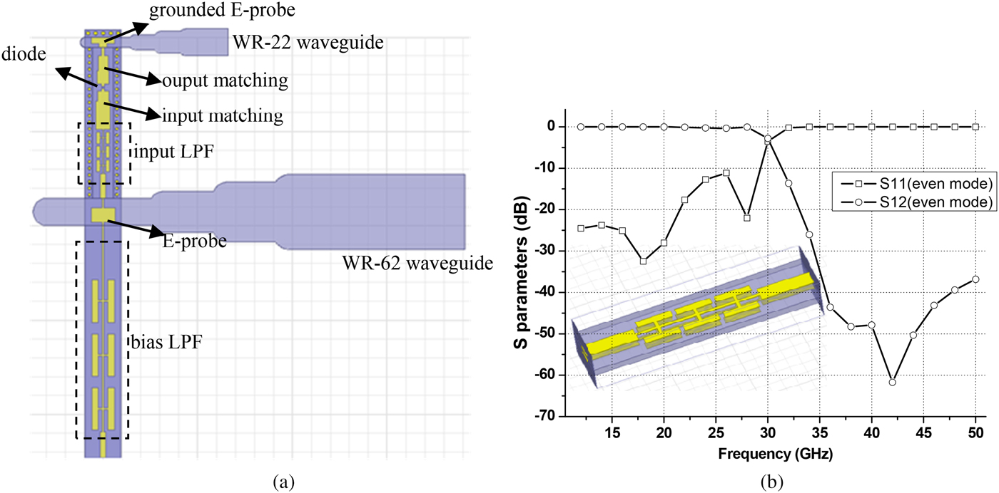
Fig. 5. (a) Prototype of Q-band balanced frequency tripler. (b) Simulation model and simulation results of the input LPF.
The simulation model and results of the input three-step hammer-head LPF are shown in Fig. 5(b). The return loss is <−20 dB at frequencies from 14 to 15 GHz, and the out-of-band rejection at frequencies from 42 to 45 GHz is more than 45 dB. It means most power of the third harmonic produced by the diodes flows to the output waveguide.
The bias LPF is used to prevent the input signal from leaking to the bias port. The simulated results of the bias LPF has been shown in Fig. 2. The leaked power to the bias port is <−40 dB, so most of the input power is utilized to drive the diodes.
The width and height of the channel supporting the coupled SSS is restricted, in case higher order mode signals pass through the channel directly to the output waveguide. Thus, the cut-off frequency of the channel is set much higher than the frequency of the output signal. In this design, the width of the channel is 2.2 mm, and the height is 1.6 mm. The corresponding TE10 mode cut-off frequency is about 68 GHz.
Schottky diode MA46H146 fabricated by M/A-COM is used in this design. The passive circuits of the tripler are simulated with HFSS, and scatter parameters are then exported to Advanced Design System (ADS) from Agilent. Finally, input and output matching circuits are designed based on the optimum impedance obtained from the circuit simulator. The simulated results will be given along with the measured results.
IV. PROPOSED 2N-DIODE POWER-COMBINED BALANCED TRIPLER
High output power is useful to pump high dynamic range mixer or to pump cascaded frequency multipliers at submillimeter-wave band. The conversion efficiency of passive frequency tripler at millimeter-wave band is usually lower than 10%. Part of the rest power is distributed mainly on the fifth harmonic, and the most part is absorbed by the diodes. The junction temperature rises due to excess RF power absorbed, which deteriorates the conversion efficiency, or even burn up the diode. In this case, more diodes are needed to sustain the increased input power, and in the meantime preserve high conversion efficiency. In a word, power handling capacity of Schottky diode frequency multiplier mostly depends on how many diodes are used.
In this work, a power-combined 2N-diode balanced frequency tripler is fulfilled by simply replacing the front and the back diode of the introduced tripler with N parallel diodes, respectively. The schematic of the 2N-diode tripler is shown in Fig. 6.
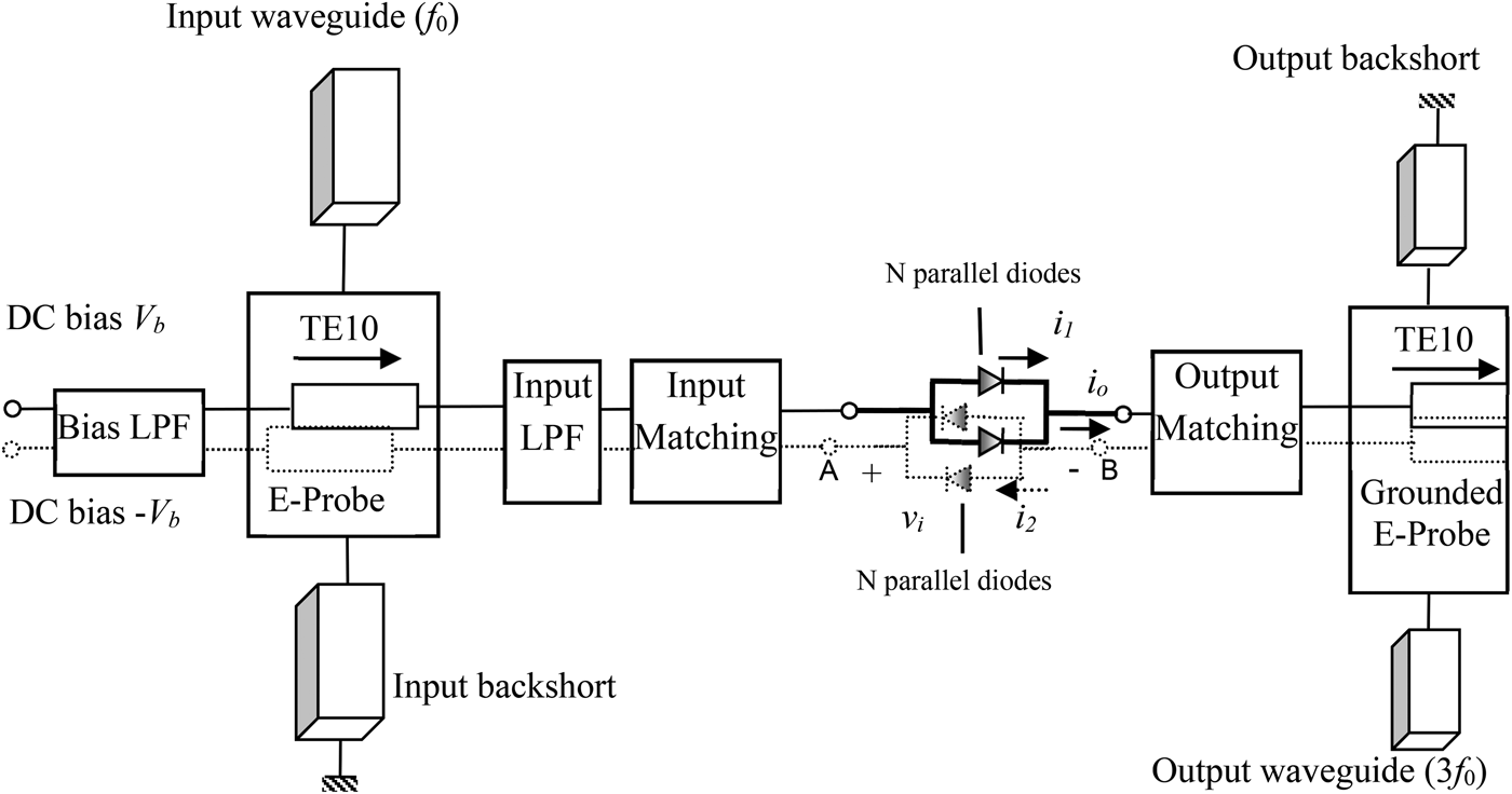
Fig. 6. Proposed 2N-diode power-combined balanced tripler with coupled SSS.
The working principles of the 2N-diode tripler can be interpreted in two ways. First, the N parallel front diodes or back diodes are equivalent to a single diode. Then a balanced frequency tripler as in Fig. 4 is obtained. However, the input power is divided equally and absorbed by 2N diodes. Thus, the power capacity of the 2N-diode tripler is N times that of the two-diode tripler. Second, if we choose any one of the front diode, we can choose another symmetrical back counterpart to form a balanced frequency tripler. Then we have N balanced triplers. The coupled SSS divides the input power into N ways in phase, and then recombine the output power in phase, too.
A) Power rating of the proposed tripler
Power rating of the proposed tripler depends on two factors, which are maximum sustainable reverse voltage of the diode and burning down temperature of the Schottky junction due to power absorbed.
First, the maximum input power is constrained by the maximum sustainable reverse voltage, v bm , of Schottky diode. The instantaneous peak input voltage must be less than v bm , or the junction of the diode will break down permanently. The balanced tripler described in [Reference Maestrini, Ward, Chattopadhyay, Schlecht and Mehdi6] uses two arms of diodes, and the diodes in each arm are in series connection. The number of the diodes in each arm determines the power handling performance. Thus, the peak input voltage is multiplied based on how many diodes are used in each arm.
However, in the proposed scheme, the peak input voltage is determined by single diode, because the diodes are in parallel connection. Maximum input power constrained by v bm is verified as below.
Let the input power is P i , and then the peak input voltage v p is
 $$v_p = \sqrt 2 \times v_{rms} = \sqrt 2 \times \sqrt {P_i R} $$
where R is assumed as 50 Ω.
The peak input voltage must be less than the maximum sustainable reverse voltage,
 $$v_p \le v_{bm}. $$
From (5) and (6), it is concluded that
 $$P_i \le \displaystyle{{v_{bm} ^2} \over {2R}}.$$
For MA46H146, v bm is 26 V, and then
 $$P_i \le 6.76\;{\rm W}{\rm.} $$
The GaAs diode will be saturated far below this power.
Second, the maximum junction temperature should not be exceeded, which is about 150°C for GaAs diode for long-term reliable operation. Most input power of the tripler turns into heat in the junction because of low conversion efficiency. The input power is divided evenly among all the diodes in the proposed tripler, so the power capacity is increased N times compared with the traditional anti-parallel diode tripler.
From the analysis above, power capacity of the proposed 2N-diode tripler is mainly constrained by the maximum junction temperature instead of the maximum sustainable reverse voltage for diode with high v bm , such as MA46H146 used in this work.
B) Other constrains of the proposed tripler
In the proposed tripler, each side of the SSS has N diodes mounted in parallel. Then N times of the width of the diode must be less than the width of the channel for proper assembly. In this work, the width of MA46H146 is 0.34 mm and the width of the channel is 2.2 mm, so six diodes can be used at most on each side of SSS.
V. PROTOTYPES OF TWO/FOUR/SIX DIODES FREQUENCY TRIPLER
The proposed tripler scheme is verified by three prototypes, with two, four, and six diodes, respectively. Split waveguide is used in these designs. The photos of the lower halves of the triplers supporting the substrates are shown in Fig. 7. The detailed bias circuit is shown in Fig. 7(e). The blue region indicates the bottom layer of the circuit, and the coppery color indicates the top layer. In order to simplify diode mounting procedure, the bottom layer bias line is lead to top layer through a metallized via. To avoid RF leakage, a LPF is mounted directly after DC connecting via. Traditional anti-parallel diode tripler with two parallel diodes is also designed for the performance comparison.

Fig. 7. Photos of four Q-band frequency triplers and detailed DC configuration. (a) Proposed tripler with two diodes; (b) proposed tripler with four diodes; (c) proposed tripler with six diodes; (d) traditional anti-parallel diode tripler; (e) detailed DC bias configuration.
The measured results are shown in Fig. 8. The maximum output power of the signal generator E8257D from Agilent is around 20 dBm. A Ku-band power amplifier is inserted between the signal generator and the tripler in order to increase the drive power of the tripler. The output power of the amplifier, followed with an isolator, is measured and adjusted to three specific values before testing the triplers, which are 25, 28, and 30 dBm at frequencies from 14 to 15 GHz. The performance of the triplers are then measured under these drive powers.
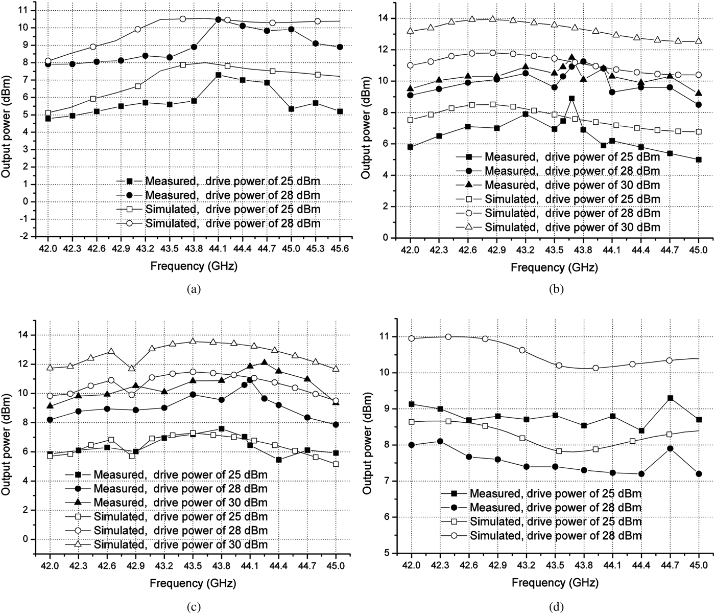
Fig. 8. Measured output power of (a) frequency tripler with two diodes, (b) frequency tripler with four diodes, (c) frequency tripler with six diodes, and (d) traditional anti-parallel diode tripler.
The measured output power of the proposed two-diode tripler is shown in Fig. 8(a). The maximum measured output powers are close to the simulated ones. Power peaks and pits are observed because of the mismatch between the tripler and power meter. Insertion loss of the transitions and matching circuits is not considered in the simulation, which results in measured power lower than the simulated one. The output power is from 8 to 10.5 dBm with 28 dBm drive power at frequencies from 42 to 45 GHz, with corresponding efficiency from 1 to 1.7%. When the drive power is increased from 28 to 30 dBm during the test, the output power of the two-diode tripler was first found unstable, and a few seconds later it dropped dramatically below −20 dBm. This is because the diodes are burn down by so much heat produced by excessive RF power absorbed. Figure 8(d) gives the simulated and measured results of the traditional two-diode anti-parallel tripler. Power compression is found from the measured output power with drive power increased from 25 to 28 dBm. While the proposed two-diode tripler works linearly under the same condition. This is because the traditional anti-parallel diode tripler is self-biased, and the proposed two-diode tripler is biased with an external DC source, which means power capacity of the proposed tripler is larger than the traditional ones with the same number of diodes, benefiting from external DC bias.
Figure 8(b) gives the simulated and measured output power of the four-diode tripler. The simulated results show that when the drive power of the tripler is increased from 25 to 28 dBm, the output power is increased correspondingly. It means the tripler operates linearly under drive power up to 28 dBm. However, the measured output power with drive power of 30 dBm is only a little higher than the one with drive power of 28 dBm. The output power is from 9 to 11.5 dBm with 30 dBm drive power at frequencies from 42 to 45 GHz, with corresponding efficiency from 0.8 to 1.4%. Power compression is clearly observed during test other than simulation. The reason of this phenomenon is that the rising junction temperature due to excessive RF power absorbed by the diodes is not considered during the simulation, which leads to increased equivalent junction series resistance [Reference Tang14]. When it comes to the six-diode tripler as shown in Fig. 8(c), the measured output power with drive power of 30 dBm is about 1 dB higher than the one with drive power of 28 dBm. The output power is from 9 to 12 dBm with 30 dBm drive power at frequencies from 42 to 45 GHz, with corresponding efficiency from 0.8 to 1.6%. Power compression is not as obvious as the four-diode tripler. During the test of traditional two-diode anti-parallel tripler when we increase the drive power from 25 to 28 dBm, we observed an obvious drop of output power. This is probably because the excessive heat slows down the electron mobility and deteriorates the performance of the diodes. In fact, we further increased the drive power from 28 to 30 dBm, and it is found that the diodes are burn down, with no output power observed.
Power compression phenomenon is further studied by measuring output power under different drive power at output frequency of 43.5 GHz, with measured results shown in Fig. 9. Maximum output power of proposed two-diode tripler is 9.2 dBm with 26.8 dBm drive power, and the output power drops to 8.7 dBm when drive power is further increased to 27.8 dBm. In traditional anti-parallel two-diode tripler, the conversion loss before saturation is approximately 1 dB better than the proposed two-diode structure. This is probably led by individual differences of the diodes and the mounting errors of the substrate and the diodes. Maximum output power of four-diode tripler is 11 dBm with 28.8 dBm drive power, and the output power drops to 10.2 dBm when drive power is increased to 29.8 dBm. Maximum output power of six-diode tripler is 12 dBm with 31.8 dBm drive power, and the output power drops to 10.4 dBm with drive power increased to 32.8 dBm. Power compression is clearly observed for all the triplers, and six-diode tripler has the maximum compression power as expected.
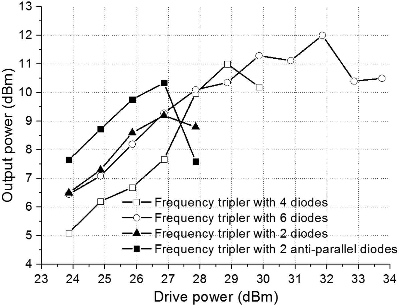
Fig. 9. Output power versus input power at for 2N-dioode tripler at 43.5 GHz output frequency.
A) Investigation on the DC bias of proposed tripler
For Schottky varactor frequency multiplier, capacitance non-linearity of the diode junction is used to produce required harmonic [Reference Faber, Chramiec and Adamski15]. The multiplier has the maximum conversion efficiency with the optimum reverse bias voltage, with a given input power and frequency. The bias circuit for the diode of frequency multiplier [16] is given in Fig. 10. V b is the external bias voltage of the voltage source, and R b is the external bias resistor. The diode's equivalent circuit is combined of an intrinsic junction and other parametric resistors, inductors, and capacitors [Reference Tang and Stake17, Reference Tang18]. The parametric inductors and capacitors are omitted in Fig. 10(a), because they have no impact on the DC bias of the diode. Then, only the intrinsic junction and the parametric series resistor, which is R s , are reserved as shown in Fig. 10(a). The actual DC bias of the diode is the bias voltage of the intrinsic junction, which is V d . The bias circuit used in Fig. 10(a) adopts a voltage source to bias the diode. Common voltage source cannot sink current when the output voltage is positive. Thus a bias resistor, R b , is added in parallel with the diode. Then the diode is reverse biased, and at the same time the bias resistor, R b , sinks current from the diode.
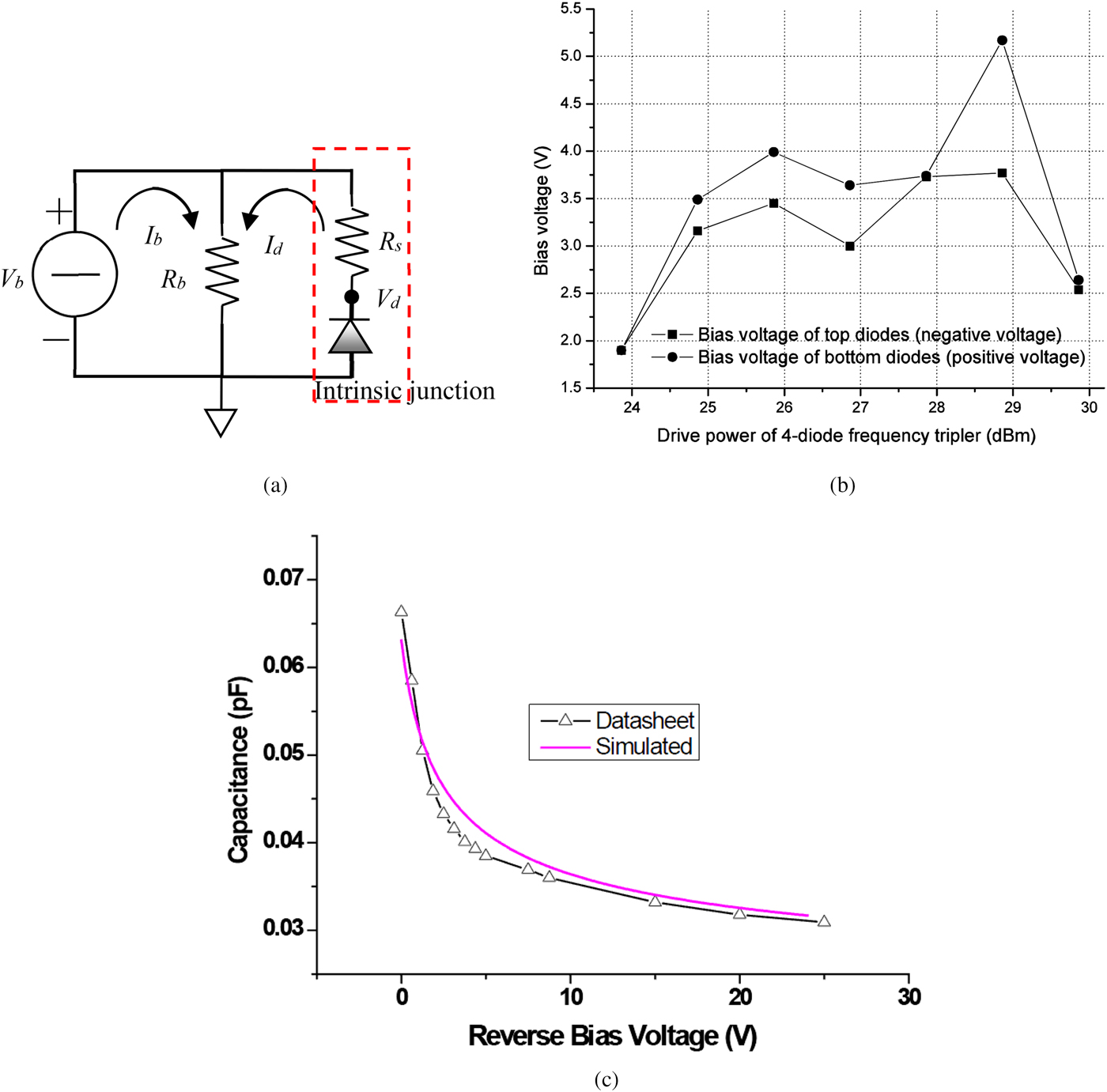
Fig. 10. (a) DC bias circuit for the diode of frequency multiplier; (b) optimum reverse bias voltage for four-diode triplers at 43.5 GHz output frequency; (c) C–V curve of MA46H146.
Optimum V d for a given diode to achieve the maximum conversion efficiency is usually around a bias point where the largest non-linearity is produced, which can be found from the C–V curve of the diode. In this design, we adopt MACOM Varactor Diode MA46H146, with the C–V curve shown in Fig. 10(c).
When the diode is driven by a RF signal, a DC current I d with direction from anode to cathode is induced. Some frequency multiplier is self-biased by this current, with V b in Fig. 10(a) equaling to zero, and the reverse bias voltage is shown in equation (8). V d is a positive voltage as expected. The resistance of R b can be set to zero, with the series resistor R s of the diode working as the bias resistor. However, the multiplier is not inherently high efficiency in this situation, because the expected bias voltage cannot be fulfilled by this series resistor.
 $$V_d = I_d \times (R_s + R_b ).$$
As for the external DC bias case, equation (9) gives the bias voltage of the intrinsic junction.
 $$V_d = V_b + I_d R_s. $$
The optimum bias voltage of a frequency multiplier is not always the same at different working frequency. With external DC biased frequency multiplier, the bias voltage V d of the intrinsic junction can be conveniently tuned to the optimum bias voltage by tuning the external bias voltage source. Thus, working bandwidth of the frequency multiplier with external DC bias is much wider than the self-biased frequency multiplier.
During the test, DC bias voltages of the proposed frequency multiplier are tuned to obtain maximum output power. Figure 10(b) gives the optimum bias voltages for the four-diode tripler under different drive power level at 43.5 GHz output frequency. Bias voltage is negative for front diodes and positive for back diodes in order to get the diodes reverse biased. The bias voltage curves in Fig. 10(b) for front and back diodes are mostly close to each other, but the bottom diodes need a bias voltage of +5 V to handle 29 dBm drive power, which is higher than expected. This is probably because of the individual difference of the diodes and the diodes mounting error.
Generally, larger input power requires higher bias voltage in order to guarantee the diode working in the varactor mode. However, it is found that the optimum bias voltage drops down when drive power is higher than 29 dBm. Actually, R s in equation (9) is not a constant, but almost proportional to the junction temperature [Reference Tang14]. Large drive power not only increases the induced current I d , but also increases the junction temperature. Thus, I d Rs in equation (9) is increased tremendously under large drive power. In order to achieve a given V d , the external bias voltage V b needs to be reduced.
From the measured results and analysis above, we draw following conclusions. First, power compression is observed during the test, and the tripler with more diodes has larger output compression power. Second, two-diode tripler failed under 30 dBm drive power due to excessive RF power absorbed by the diodes. Third, external DC bias voltage needs to be reduced when large drive power is applied to the tripler.
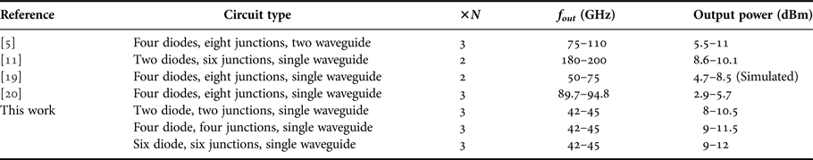
The performance of the proposed tripler is compared with other reported frequency multiplier also adopting power combining scheme, as shown in Table 1. Up to six diodes is used in the proposed tripler, and the output power can be further increased by using high-performance multi-junction diode.
Table 1. Performance comparison with other reported works.
VI. CONCLUSIONS
A 2N-diode balanced tripler is proposed in this work using coupled SSS. The front and back diodes at each side of the coupled SSS is reverse biased, respectively. Power rating of the tripler is discussed, and it mostly depends on RF power absorbed by the diodes. According to the test results, two-diode tripler failed under 30 dBm drive power, while four-diode and six-diode tripler work properly. Tripler with more diodes brings larger output compression power. External bias voltages can be applied to both the front and back diodes to optimize the output power, and the external bias voltages need to be reduced when large drive power is applied.
The proposed 2N-diode tripler is useful for millimeter-wave and submillimeter-wave application when large power capacity is required.
ACKNOWLEDGEMENT
This work is supported by National Natural Science Foundation of China (Grant No. 61401091).
 Yinjie Cui was born in Nanjing, Jiangsu Province, China, in 1986. He received the B.S. and M.S. degrees in electrical engineering from Southeast University, Nanjing, China, in 2008 and 2011, respectively, where he is currently working toward the Ph.D. degree. His research interests are microwave and millimeter-wave circuits, metamaterial structures, and antennas design.
 Jian Guo was born in Yangzhou, Jiangsu Province, China, in 1982. He received the B.S. degree in Information Engineering from Southeast University, Nanjing, China, in 2005, and Ph.D. degree in Electromagnetic and Microwave Technology from Southeast University, Nanjing, China, in 2012. He is currently working at State Key Laboratory of Millimeter Waves, Southeast University, Nanjing, China. His main research fields are electromagnetic theory and applications, and millimeter-wave and Terahertz circuits.
 Jie Xu received the B.S. and M.S. degrees in electrical engineering from Southeast University, Nanjing, China, in 2008 and 2011, respectively, where he is currently working toward the Ph.D. degree. His research interests include microwave and millimeter-wave circuits, metamaterial structures, and antennas design.
 Hao Chi Zhang was born in January 1991, in Zhejiang, China. He received the B.Eng. degrees in electrical engineering from University of Electronic Science and Technology of China, Chengdu, China, in 2013. He is currently working towards the Ph.D. degree in electromagnetic and microwave technology from Southeast University, Nanjing, China. His research interests include microwave and millimeter wave circuits and antennas technology, Surface plasmons and metamaterials.
 Xiao wei Zhu received the B.E., M.E., and Ph.D. degrees in radio engineering from Southeast University, Nanjing, China, in 1984, 1996, and 2000, respectively. Since 1984, he has been with Southeast University, Nanjing, China, where he is currently a Professor with the School of Information Science and Engineering. He has authored or coauthored over 50 technical publications. His research interests include RF and antenna technologies for mobile communications and microwave and millimeter-wave theory and technology. Dr. Zhu was the recipient of the 1994 First-Class Science and Technology Progress Prize presented by the Ministry of Education of China and the 2003 Second-Class Science and Technology Progress Prize of Jiangsu Province, China.
 Cheng Qian received the B.E. and M.E. degrees in radio engineering from Southeast University, Nanjing, China. He is currently engaged in research and teaching of microwave and millimeter wave technology at the State Key Laboratory of Millimeter wave, Southeast University.


