
I. INTRODUCTION
Radiofrequency (RF) amplifiers are one of the most critical components in almost all types of wireless applications. Each application has different requirements depending on frequency and type of input signal, etc. For each of specific purpose, they are expected to provide suitable output power and gain, while achieving acceptable efficiency under application-specific linearity considerations [Reference Mohammadi and Ghannouchi1].
On the other hand, the request on wireless communication systems is forcing multi-band transceivers to deal with several services in the only terminal. Owing to the current demand on multi-frequency systems over several wireless communication bands, systems simultaneously working at some of the following bands (GSM, TETRA, DCS, PCS, IMT-2000, WLAN, or UWB) are currently being developed and are widely used in new portable wireless handsets [Reference Mohammadi and Ghannouchi1].
Then, due to these drawbacks, the availability of multi-frequency high linearity and efficiency amplifiers would be welcome. Some attempts have been undertaken in order to achieve that goal. In this way, the use of switches [Reference Fukuda2], varying lumped components [Reference Ujie, Sato and Ishihara3], or diplexers [Reference Sokal and Sokal4] have been proposed as potential techniques for achieving dual-frequency high-efficiency amplifiers.
During last years, the appearance of Composite Right/Left-Handed Transmission Lines (CRLH TLs) has opened new possibilities in the design of multi-band amplifiers [Reference Lin, Devincentis, Caloz and Itoh5]. Essentially CRLH structures, which are constituted by a left-handed (LH) series capacitance, shunt inductance in addition to the conventional right-handed (RH) series inductance, and shunt capacitance, along with their various microwave applications [Reference Caloz and Itoh6].
In [Reference Mata-Contrera, Camacho-Peñalosa and Martín-Guerrero7], a distributed amplifier based on the active coupling of two artificial composed of RH/LH TLs has been presented. This reported work shows that it is possible to improve the isolation between bands by means of a non-uniform distribution of the devices’ transconductance.
A novel extended composite RH/LH (E-CRLH) TL metamaterial structure, constituted by the combination of the conventional CRLH (C-CRLH) and the recently introduced dual CRLH (D-CRLH) prototypes, is proposed. Microwave devices by E-CRLH structure can be quad-band (QB)[Reference Keshavarz, Mohammadi and Abdipour8].
In this paper, a new type of quad-band-coupled lines (QB CLs) is presented. These with closely placing two E-CRLH lines in parallel are obtained that can operate with nearly 0 dB power coupling level. The proposed QB CLs operates at four frequencies; two frequencies in the backward direction and the other two frequencies in the forward direction.
Then, we use QB CLs for designing quad-band amplifier (QBA) with high linearity. The proposed structure consists of two QB CLs and two amplifiers. In the proposed QBA, four frequency bands come into the one of the proposed CLs as multiplexer and two dual-band output signals are amplified with two amplifiers. Finally, two amplified signals are demultiplexing and coming out by means of the other CLs. In this paper, the design process is clearly discussed and the analytical equations are derived.
The organization of this paper is as the following. At first, the principle of the E-CRLH TL and their property are presented. Then, the proposed QB E-CRLH CLs are introduced and design procedures are presented. Furthermore, the proposed linearity improved QBA is presented and is validated by simulation and measurement results.
II. QB E-CRLH-COUPLED LINES THEORY
Figure 1 shows the proposed E-CRLH CLs and its equivalent circuit model. As shown in Fig. 1(b), C m represents the mutual capacitance between E-CRLH TLs. In addition, other lumped elements that presented in Fig. 1(b) are ∏ equivalent circuit model elements of E-CRLH TLs [Reference Keshavarz, Mohammadi and Abdipour8]. It should be stated that all of the parameters in the circuit model are per unit length quantities.

Fig. 1. (a) E-CRLH CLs, (b) equivalent circuit model of E-CRLH CLs.
From Fig. 1, series impedance (Z) and parallel admittance (Y) of an E-CRLH unit cell can be derived as following [Reference Keshavarz, Mohammadi and Abdipour8]:
 $$\eqalign{Z = j\omega L_R^c \left( {1 - \displaystyle{{\omega _{cs}^2} \over {\omega ^2}}} \right) - \displaystyle{j \over {\omega C_L^d \left( {1 - \left( {\displaystyle{{\omega _{dp}^2} \over {\omega ^2}}} \right)} \right)}}\;,} $$
 $$Y = j\omega C_R^c \left( {1 - \displaystyle{{\omega _{cp}^2} \over {\omega ^2}}} \right) - \displaystyle{j \over {\omega L_L^d \left( {1 - \left( {{{\omega _{ds}^2} / {\omega ^2}}} \right)} \right)}}, $$
where
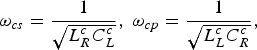 $$\omega _{cs} = \displaystyle{1 \over {\sqrt {L_R^c C_L^c}}}, \; \omega _{cp} = \displaystyle{1 \over {\sqrt {L_L^c C_R^c}}}, $$
 $$\; \omega _{dp} = \displaystyle{1 \over {\sqrt {L_R^d C_L^d}}}, \; \omega _{ds} = \displaystyle{1 \over {\sqrt {L_L^d C_R^d}}}, $$
 $$\omega _{dscp} = \displaystyle{1 \over {\sqrt {L_L^d C_R^c}}}, \; \; \omega _{csdp} = \displaystyle{1 \over {\sqrt {L_R^c C_L^d}}}, $$
 $$\omega _{dp} = \omega _{ds}, \; \omega _{cp} = \omega _{cs} \; ({\rm balance\;} \,{\rm conditions})\;. $$
Therefore, for an E-CRLH TL, the propagation constant is equal to [Reference Eleftheriades9]:
 $$\cos (\beta l) = 1 + ZY/2, $$
where l is the physical length of the unit cell.
The Bloch impedance of a periodic transmission line is presented in [Reference Keshavarz, Mohammadi and Abdipour8] as:
 $$Z_B = \sqrt {\displaystyle{Z \over Y}} \sqrt {1 + \displaystyle{{ZY} \over 4}}. $$
When the dimension of the unit cell is very small
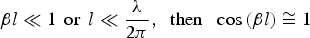 $\beta l \ll 1\,\; {\rm or}\,\; l \ll \displaystyle{\lambda \over {2\pi}}, \; \;{\rm then\;} \,\,\cos \left( {\beta l} \right) \cong 1$
and according to equation (8):
$\beta l \ll 1\,\; {\rm or}\,\; l \ll \displaystyle{\lambda \over {2\pi}}, \; \;{\rm then\;} \,\,\cos \left( {\beta l} \right) \cong 1$
and according to equation (8):
 $$ZY \cong 0 \to Z_B = \sqrt {\displaystyle{Z \over Y}} \sqrt {1 + 0} = \sqrt {\displaystyle{Z \over Y}}. $$
In this case, the Bloch impedance is approximately equal to the characteristic impedance Z B ≅ Z c .
However, in the coupled-line couplers, input matching condition to terminations of impedance Z c is obtained under the condition given by [Reference Pozar10]:
 $$Z_c = \sqrt {Z_{ce} Z_{co}}, $$
where Z ce and Z co are even- and odd-mode characteristic impedances of the CLs, respectively.
In design procedure, Z ce and Z co can be obtained from conventional expressions as [Reference Mongia, Bahl and Bhartia11]:
 $$Z_{ce} \cong \sqrt {\displaystyle{{Z_e} \over {Y_e}}}, \,Z_{co} \cong \sqrt {\displaystyle{{Z_o} \over {Y_o}}}, $$
where Z e and Y e are the series impedance and parallel admittance of an E-CRLH unit cell in the even mode, respectively, and are found as:
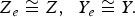 $$Z_e \cong Z,\; \; Y_e \cong Y.$$
Also Z o and Y o are the series impedance and parallel admittance of an E-CRLH unit cell in the odd mode, respectively, and are found as:
 $$Z_o \cong Z,\; \; Y_o \cong Y + Y_m, $$
where Y m is the influence of C m that is added to the parallel admittance Y and is equal to:
 $$Y_m = 2j\omega C_m \left( {1 - \displaystyle{{\omega _{cp}^2} \over {\omega ^2}}} \right).$$
Furthermore, according to (12) and (13) the characteristic impedance in equation (10) could be rewritten as:
 $$Z_c^4 = \displaystyle{{Z^2} \over {Y^2 + YY_m}} \;. $$
Currently, we want to design a QB E-CRLH CLs that has two output ports. The signal is going out from port #4 (forward direction) at frequencies F 2 and F 4 and from port #3 (backward direction) at frequencies F 1 and F 3 (Fig. 1). In addition, port #2 is isolated. Therefore, these CLs exhibit such as QB couplers.
In the E-CRLH CLs, similar to the conventional edge-coupled couplers, the backward wave (S 31) and forward wave (S 41) coupling coefficients are [Reference Mongia, Bahl and Bhartia11]:
 $$S_{31} = \displaystyle{{jk{\rm sin}\theta} \over {\sqrt {1 - k^2} {\rm cos}\theta + j{\rm sin}\theta}}, $$
 $$S_{41} = - je^{\displaystyle{{ - j\left( {\beta _e + \beta _o} \right)l} \over 2}} {\rm sin}\left[ {\displaystyle{{((\beta _e - \beta _o )l)} \over 2}} \right], $$
where
 $$k = \displaystyle{{Z_{ce} - Z_{co}} \over {Z_{ce} + Z_{co}}}, \,\theta = \beta l$$
and β e and β o are propagation constants of the even and odd modes, respectively, and l is the length of the structure. In addition, the direct coefficient is equal to:
 $$S_{21} = \displaystyle{{\sqrt {1 - k^2}} \over {\sqrt {1 - k^2} {\rm cos}\theta + j{\rm sin}\theta}}. $$
Now, we discuss about the forward and backward directions coupling in the proposed QB CLs and the design equations will be derived.
Forward direction coupling: In the proposed E-CRLH CLs, we want the coupling coefficient in the forward wave equals to 0 dB at frequencies F 2 and F 4. So, according to (17):
 $$l = \displaystyle{\pi \over {\beta _e - \beta _o}} \to \theta _e - \theta _o = \pi \to \cos \theta _e = - \cos \theta _o. $$
Therefore, substituting (7), (12), and (13) into (20) result in:
 $$(1 + Z_e Y_e /2) = - \left( {1 + Z_o Y_o /2} \right)\; \to {\rm cos}\theta _i = - ZY_m /4.$$
Equation (21) states two conditions for
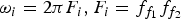
 $\omega _i = 2\pi F_i, \; \; F_2 = f_{f_1}, F_4 = f_{f_2}. $
The f
f1 and f
f2 are operation frequencies in the forward direction coupling.
$\omega _i = 2\pi F_i, \; \; F_2 = f_{f_1}, F_4 = f_{f_2}. $
The f
f1 and f
f2 are operation frequencies in the forward direction coupling.
From (7), (15), and (21) the required condition for 0 dB forward coupling coefficient at frequency f i is:
 $$Y_m^2 = \displaystyle{{64({\rm cos}\theta _i )^4} \over {Z_c^4 (1 - ({\rm cos}\theta _i )^2 )}} = - C_i^2. $$
Then, (14) and (22) establish the following polynomial equation:
 $$2\omega _i^2 x_1 - 2x_2 = C_i \omega _i, $$
where x
1 = C
m
and
 $x_2 = C_m \omega _{cp}^2 $
are unknown parameters and
$x_2 = C_m \omega _{cp}^2 $
are unknown parameters and
 $\omega _i = 2\pi F_i, F_i = f_{f_1} f_{f_2} $
.
$\omega _i = 2\pi F_i, F_i = f_{f_1} f_{f_2} $
.
Backward direction coupling: From (16), it is clear that complete power can be transferred between lines in backward direction if θ = 90°, thus:
 $$S_{31} = k = \displaystyle{{1 - \sqrt {(Y/Y_o )}} \over {1 + \sqrt {(Y/Y_o )}}} = \displaystyle{{1 - \sqrt {(Y/(Y_m + Y))}} \over {1 + \sqrt {(Y/Y_m + Y)}}}. $$
According to (24), the maximum of k (k max = 1) is occurred when Y = 0. Setting (2) equals to zero produces below polynomial equation.
 $$\omega _i^2 x_3 - x_4 = \omega _i^4, $$
where
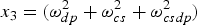 $x_3 = (\omega _{dp}^2 + \omega _{cs}^2 + \omega _{csdp}^2 )$
and
$x_3 = (\omega _{dp}^2 + \omega _{cs}^2 + \omega _{csdp}^2 )$
and
 $x_4 = \omega _{dp}^2 \omega _{cs}^2 $
are unknown parameters and
$x_4 = \omega _{dp}^2 \omega _{cs}^2 $
are unknown parameters and
 $\omega _i = 2\pi F_i, \; F_i = f_{b_1}, f_{b_2} $
. The f
b1 and f
b2 are operation frequencies in the backward direction coupling.
$\omega _i = 2\pi F_i, \; F_i = f_{b_1}, f_{b_2} $
. The f
b1 and f
b2 are operation frequencies in the backward direction coupling.
Then, according to (23) and (25), we have four equations and four unknown parameters and the equations set are as below:
 $$\left[ A \right].\left[ X \right] = \left[ D \right],$$
where
 $$A = \left[ {\matrix{ {\matrix{ {2\omega _{f_1} ^2} & { - 2} \cr {2\omega _{f_2} ^2} & { - 2} \cr}} & {\matrix{ 0 & {\; \; \; 0} \cr 0 & {\; \; \; 0} \cr}} \cr {\matrix{ 0 & {\; \; \; \; \; \; 0} \cr 0 & {\; \; \; \; \; \; 0} \cr}} & {\matrix{ {\omega _{b_1} ^2} & { - 1} \cr {\omega _{b_2} ^2} & { - 1} \cr}} \cr}} \right],\; \,D = \left[ {\matrix{ {C_{f_1} \omega _{f1}} \cr {C_{f_2} \omega _{f_2}} \cr {\omega _{b_1} ^4} \cr {\omega _{b_2} ^4} \cr}} \right]$$
and
 $$\left[ X \right] = \left[ {\matrix{ {x_1} \cr {x_2} \cr {x_3} \cr {x_4} \cr}} \right] = \left[ {\matrix{ {C_m} \cr {C_m \omega _{cp}^2} \cr {\left( {\omega _{dp}^2 + \omega _{cp}^2 + \omega _{dscp}^2} \right)} \cr {\omega _{dp}^2 \omega _{cs}^2} \cr}} \right]\; \;. \; \; \; $$
A set of four linear equations could be solved under balance conditions (6) simply as follows:
 $$\left\{ {\matrix{ {C_m = x_1,} \cr {\omega _{cs}^2 = \omega _{cp}^2 = x_2 /x_1,} \cr {\omega _{ds}^2 = \omega _{dp}^2 = \left( {x_1 x_4} \right)/x_2,} \cr {\omega _{dscp}^2 = x_3 - \omega _{dp}^2 - \omega _{cp}^2.} \cr}} \right.$$
According to C
m
the gap spacing (S) between the E-CRLH-coupled lines is determined. Nevertheless, for extracting eight lumped elements of E-CRLH unit cell of Fig. 1 matching condition (15) is necessary at four operation frequencies
 $f_{f_1}, f_{f_2}, f_{b_1}, \,and\,f_{b_2} $
.
$f_{f_1}, f_{f_2}, f_{b_1}, \,and\,f_{b_2} $
.
III. PROPOSED QBA THEORY
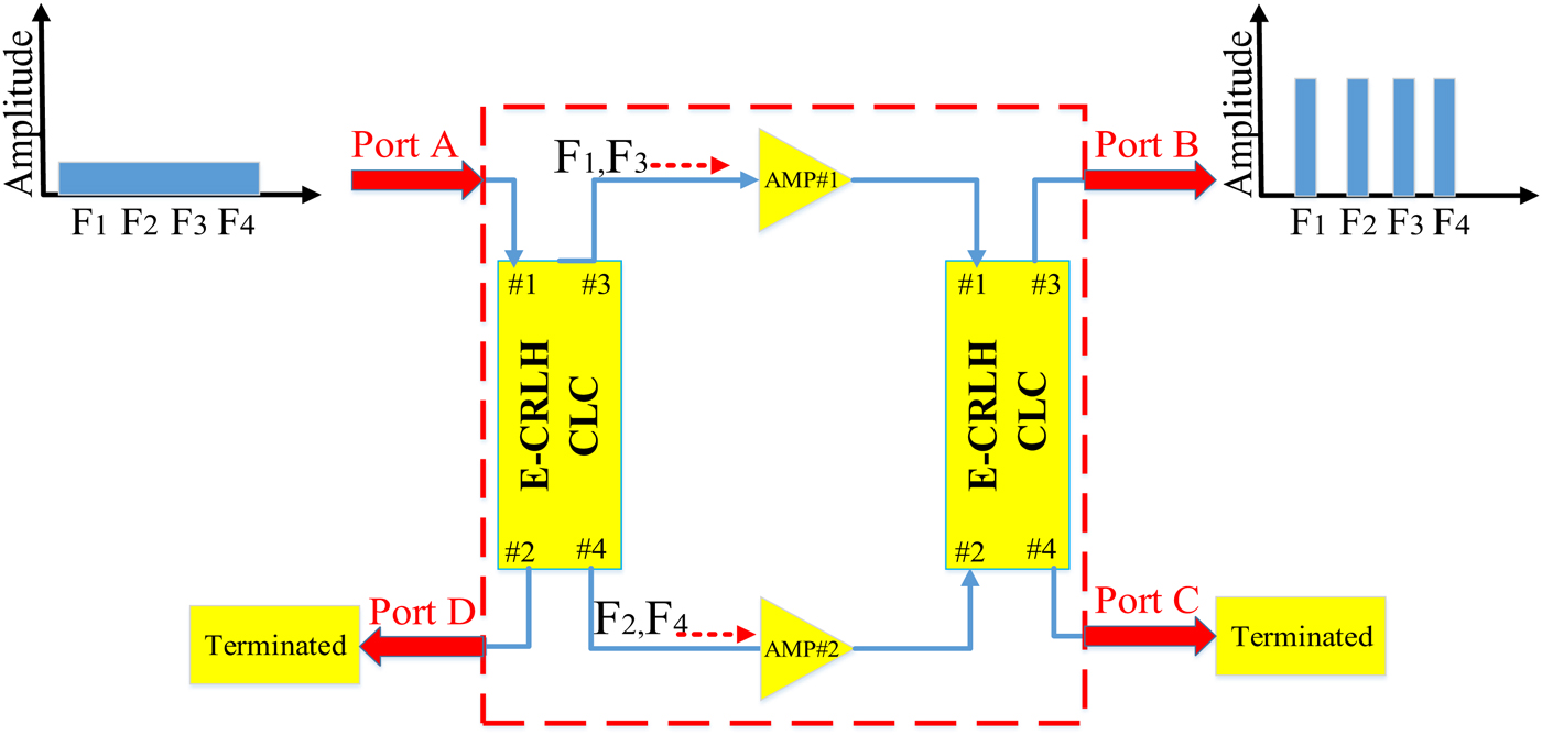
Equations Fig. 2 shows the proposed application of the QB CLs in the QBA. According to this figure when a wide band spectrum that including F 1, F 2, F 3, and F 4 frequency bands incoming from port A then the output signal has QB spectrum and coming out from port B. Because first CLs operates as multiplexer and its dual-band output signals are amplified with two amplifiers. Finally, two amplified signals are demultiplexed by means of the other CLs and coming out from port B. In addition, ports C and D are loaded with 50 Ω.

Fig. 2. The principle of dual-band duplexer (
 $F_1 = f_{b_1}, \; \,F_3 = f_{b_2}, \,\; F_2 = f_{f_1}, \; \,F_4 = f_{f_2} $
).
$F_1 = f_{b_1}, \; \,F_3 = f_{b_2}, \,\; F_2 = f_{f_1}, \; \,F_4 = f_{f_2} $
).
This idea can be used in power amplifier or low-noise amplifier. Traditionally, the nonlinearity of an RF amplifier is described by third-order intermodulation point (IP3) or, equivalently, by the 1 dB compression point. However, the nonlinearity control is specified by the out-of-band power emission levels. Out-of-band emission is also called spectrum regrowth. Spectral regrowth is a condition that interferes with signals in adjacent frequency bands and can be reduced by using power amplifier linearization techniques [Reference Wu, Testa and Larkin12].
In power amplifier applications instead of four frequency bands, only two frequency bands push into each amplifier. Therefore, intermodulation components decrease and linearity improve. Due to every other frequency bands are driven to each amplifier, so third-order intermodulation components are out of frequency bands. This concept is shown in Fig. 3. According to this figure, the third-order intermodulation components in the proposed QBA reduce to one component near the frequency bands. Whereas, the third-order intermodulation components in the conventional amplifier distort the main operational frequency bands and we must use bank filter and isolated amplifiers for each frequency bands.
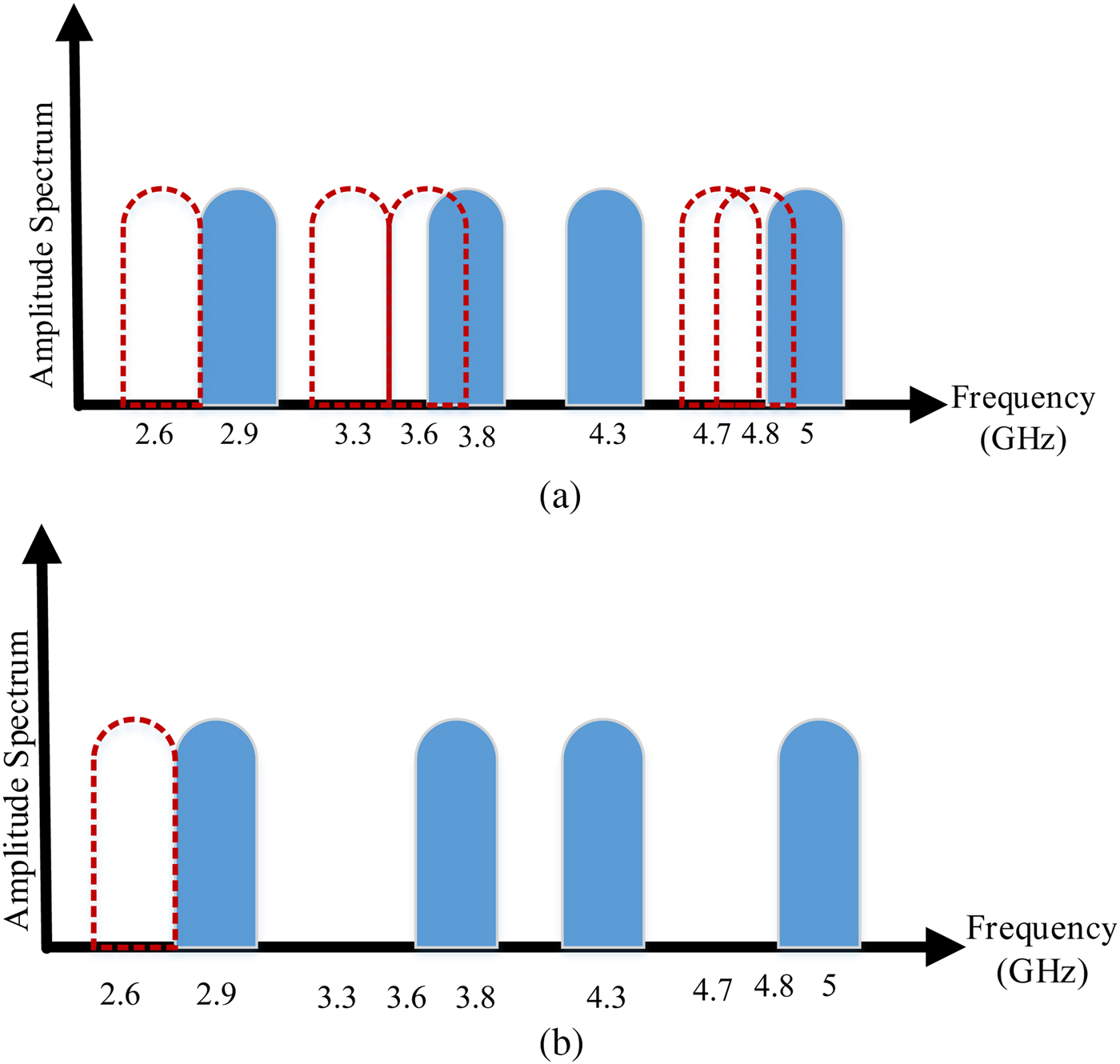
Fig. 3. Amplitude spectrum of the operational frequency bands (F 1 = 2.9 GHz, F 2 = 3.8 GHz, F 3 = 4.3 GHz, F 4 = 5 GHz) and their intermodulation components (dashed); (a) conventional amplifier, (b) proposed QBA.
In low-noise amplifier applications, the proposed structure can improve the sensitivity up to 6 dB. As in the conventional receivers when four frequency bands need to receive simultaneously, we cannot use switches before the bank filter. As a result, splitter or multiplexer must be used before the bank filter (Fig. 4) [Reference Chen, Huang, Chou and Wu13, Reference Kim, Kim, Ryu, Kim, Park and Park14]. Using splitter leads to 6 dB reduction in the receiver sensitivity. Consequently, multiplexer is better solution for this concept. In the proposed structure, bank filter and multiplexer are combined with each other.
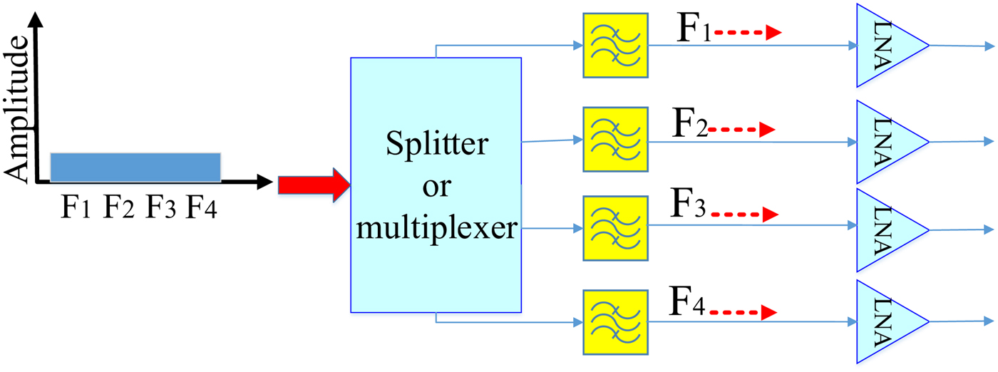
Fig. 4. Conventional QB receiver configuration (
 $F_1 = f_{b_1}, \; \,F_3 = f_{b_2}, \; \,F_2 = f_{f_1}, \,\; and\,F_4 = f_{f_2} $
).
$F_1 = f_{b_1}, \; \,F_3 = f_{b_2}, \; \,F_2 = f_{f_1}, \,\; and\,F_4 = f_{f_2} $
).
IV. SIMULATION AND EXPERIMENTAL RESULTS
Citations to confirm the proposed structure, a QB CLs and a QBA based on the design procedure and presented expressions realized (Fig. 5). The structures has been fabricated on RO-4003 substrate with ε r = 3.38, thickness of 20 mil and tan δ = 0.003. The QBA amplifiers work in class-A with the PHEMT technology amplifier (MGA-82563). The amplifiers is biased in VGS =0 V, VDS = 3 V, and IDS = 80 mA. The resistive feedback in this amplifier ensures stability (K > 1 and |Δ| < 1) over all frequencies and temperatures.

Fig. 5. Fabricated structures on the RO-4003 substrate, ε r = 3.38, thickness of 32 mil and tan δ = 0.003; (a) QB CLs, (b) QBA.
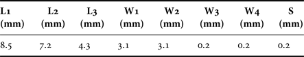
The proposed structures operate at four frequencies: F 1 = 2.9 GHz, F 2 = 3.8 GHz, F 3 = 4.3 GHz, and F 4 = 5 GHz. According to these conditions, the lumped element components in Fig. 1 are calculated (Table 1). The dimensions of the proposed structure (Fig. 1) are presented in Table 2.
Table 1. Lumped element values of Fig. 1.

Table 2. Dimension of the proposed dual-band duplexer (Fig. 1).
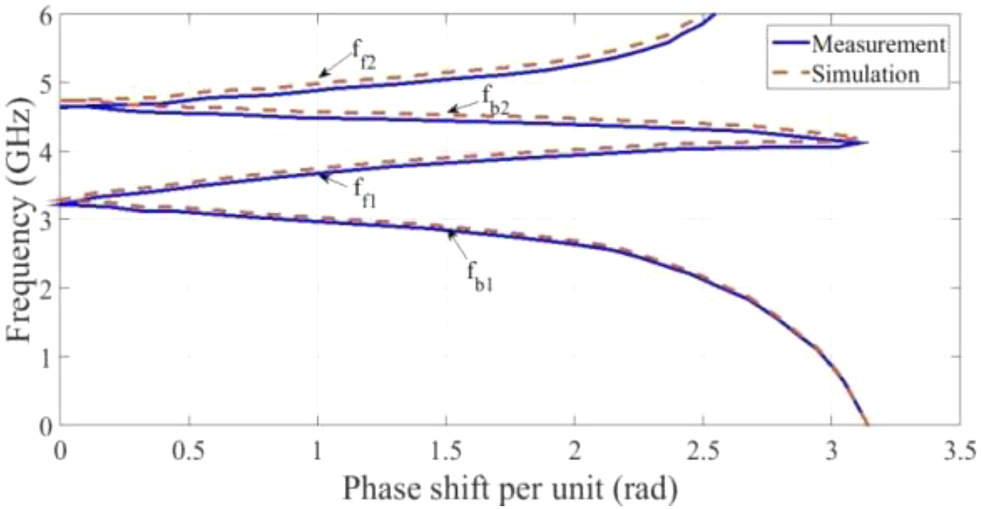
The absolute value of the dispersion curves of the proposed E-CRLH CLs unit cell (simulation and measurement) is presented in Fig. 6. Figure 7 presents the full-wave simulated (by using Agilent ADS software) and measured S-parameters for the QB CLs of Fig. 5(a). Using these figures, an amplitude balance of ±1 dB over a bandwidth of 300 MHz, a matching (−10 dB bandwidth) and an isolation at least −15 dB and −20 dB over bandwidth of operation in backward and forward direction are observed, respectively.

Fig. 6. Dispersion curve of the E-CRLH unit cell (full-wave simulation and measurement results).

Fig. 7. (a) |S 11 | and |S 21 |, (b) |S 31 | and |S 41 |, (c) |S 34 | parameters of the proposed dual-band duplexer.
Furthermore, a QBA with at least 300 MHz bandwidth around the design frequencies is realized in the measured prototype (Fig. 8). As can be seen, a QBA around the design frequencies has been achieved. The proposed QBA nearly achieves 12 dB gain and return loss better than 15 dB in operation frequency bands. Excellent agreement can be observed between simulated and experimental results.

Fig. 8. (a) |S AA | and |S BA |, (b) |S CA | and |S DA |, parameters of the proposed QBA.
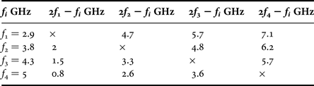
The intermodulation components of the four operation frequency bands are presented in Table 3. According to this table when four operational frequencies with 300 MHz bandwidth drive to the conventional amplifier there are some intermodulation components near to the operational frequencies. In band intermodulation components are marked in Table 3. In addition, Fig. 9 exhibits simulation and measurement results of the intermodulation components of the proposed QBA and conventional amplifier. According to this figure, intermodulation components in the proposed QBA decrease at least 50 dB proper to the conventional amplifier. Figure 10 shows the measured power-added efficiency (PAE) of the proposed QBA at four frequency bands. According to this figure, the PAE is better than 57% in pick power at all four frequency bands.

Fig. 9. (a) 2 F 1 − F 2, (b) 2 F 2 − F 3, (c) 2 F 3 − F 4, intermodulation components levels of the proposed QBA and conventional amplifier for F 1 = 2.9 GHz, F 2 = 3.8 GHz, F 3 = 4.3 GHz, and F 4 = 5 GHz (simulation and measurement results).
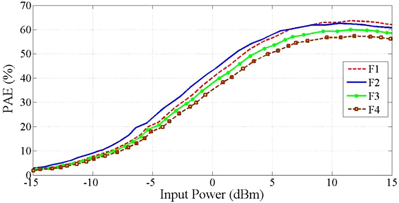
Fig. 10. Measured PAE of the proposed QBA for F 1 = 2.9 GHz, F 2 = 3.8 GHz, F 3 = 4.3 GHz, and F 4 = 5 GHz.
Table 3. Intermodulation components of the operational frequencies.
V. CONCLUSION
In this paper, we present a new technique for realizing a QBA. New QBA consists of two QB E-CRLH coupled lines and two amplifiers. Designed and fabricated QBA at center frequencies F 1 = 2.9 GHz, F 2 = 3.8 GHz, F 3 = 4.3 GHz, and F 4 = 5 GHz exhibits a matching (15 dB) bandwidth of over 300 MHz and at least 12 dB gain operation frequency bands. The length and the width of the proposed structure are approximately 7.7 and 2.4 cm, respectively. The intermodulation components of the proposed QBA decreases at least 50 dB proper to the conventional amplifier and linearity improve. Due to the multiband, compact size, and linearity improvement, the proposed QBA is well suitable for microwave and millimeter-wave-integrated circuits, multi-standard communication systems and many kinds of transceivers.
 Rasool Keshavarz received the B.Sc. degree in Electrical Engineering from Shiraz University, Shiraz, Iran, in 2004 and the M.S. degree in Electrical Engineering from Shahid Bahonar University of Kerman, Kerman, Iran, in 2007. He is currently working toward the Ph.D. degree at the Amirkabir University of Technology, Tehran, Iran. His research interests are Metamaterial, RF/Microwave circuits design and multi-standard systems. He is currently working on multi-standard six-port transceivers based on E-CRLH structures.
 Abbas Mohammadi (M'88-SM'08) received his B.Sc. degree in Electrical Engineering from Tehran University, Iran in 1988, and his M.Sc. and Ph.D. degrees in Electrical Engineering from the University of Saskatchewan, Canada, in 1995 and 1999, respectively. Since March 2000, he has been with the Electrical Engineering Department of Amirkabir University of Technology (Tehran Polytechnic), Tehran, Iran, where he is currently a professor. He is a senior member of IEEE. Dr. Mohammadi has been an ICORE visiting professor in Electrical and Computer Engineering Department of the University of Calgary, Canada and Nokia visiting professor in Tampere University of Technology, Finland. He has co-authored, Six-port Technique with Microwave and Wireless Applications (Artech House, 2009) and RF Transceiver design for MIMO Wireless Communications (Springer, 2012). His current research interests include broadband wireless communications, adaptive modulation, MIMO Systems, Mesh and Ad Hoc Networks, Microwave and Wireless Subsystems, Software Design Radio, and advanced wireless transceiver architectures.
 Abdolali Abdipour was born in Alashtar, Iran, in 1966. He received his B.Sc. degree in electrical engineering from Tehran University, Tehran, Iran, in 1989, his M.Sc. degree in Electronics from Limoges University, Limoges, France, in 1992, and his Ph.D. degree in Electronic Engineering from Paris XI University, Paris, France, in 1996. He is currently a professor with the Electrical Engineering Department, Amirkabir University of Technology (Tehran Polytechnic), Tehran, Iran. He has authored five books, Noise in Electronic Communication: Modeling, Analysis and Measurement, Transmission Lines, Active Transmission Lines in Electronics and Communications: Modeling and Analysis, Communication Circuits (Nonlinear analysis, design, and simulation), and High frequency field effect transistors (Electronic-Electromagnetics modeling and analysis). His research areas include wireless communication systems (RF technology and transceivers), RF/microwave/millimeter-wave circuit and system design, electromagnetic (EM) modeling of active devices and circuits, high-frequency electronics (signal and noise), nonlinear modeling, and analysis of microwave devices and circuits.