


I. INTRODUCTION
Differential signaling becomes increasingly popular in microwave circuits due to superior-noise immunity, better spurious response, decreased second-order non-linearity and improved stability. In order to characterize differential devices, the mixed-mode S-parameters theory has been formulated [Reference Bockelman and Eisenstadt1]. Measurement techniques for on-wafer characterization of differential devices using a pure-mode vector network analyzer have been developed [Reference Zwick and Pfeiffer2]. Furthermore, an advanced calibration technique has been proposed for characterization of multiport devices by means of multimode networks [Reference Seguinot3].
Accurate on-wafer S-parameter vector network analyzer (VNA) measurement of differential devices at microwave and millimeter-wave frequencies is a challenge. Usually, the measurement reference planes are set by classical off-wafer calibration techniques such as Short-Open-Load-Thru (SOLT), Line-Reflect-Reflect-Match (LRRM), or Thru-Reflect-Line (TRL). However, it is often not possible to set the reference planes directly at the measured devices. Thus, de-embedding techniques have to be applied to remove the impact of any error network between the calibration reference plane and the measured device. It is usually performed by well-known techniques, such as Short-Open or Thru.
The on-wafer de-embedding techniques can be divided into two categories. The first category consists of techniques based on equivalent lumped-element circuit models such as Short-Open, the three-step or the four-step method. These approaches assume a specific lumped-element model of interconnects. This reduces the de-embedding accuracy at higher frequencies. The second category consists of cascade-based two-port techniques, such as Thru-Line (TL) [Reference Steer4] or TRL [Reference Engen and Hoer5]. These techniques allow to perform de-embedding without modeling of the internal structure of the error network. Thus, they are applicable up to higher frequencies and offer much better accuracy than the techniques based on equivalent lumped-element circuits.
However, the TRL method has the disadvantage of data discontinuities at the band edges related to the physical length of the line standard. This can be resolved by using the multi-line TRL [Reference Marks6] technique, which applies multiple line standards to cover a wide frequency range. The TL method is a special case of the TRL method, which assumes identical error boxes. As a result, it needs one standard less. This simplifies the de-embedding procedure and saves the manufacturing costs of the chips. Furthermore, the result of both TL and TRL de-embedding methods is referenced to an unknown characteristic impedance of the reference planes.
In this paper, we present analytical considerations on the applicability of the classical two-port cascade-based techniques such as TL or TRL for de-embedding of differential devices. This follows as a reasonable continuation to the work presented in [Reference Issakov, Wojnowski, Thiede and Maurer7], where the extension of the Thru technique for differential devices is proposed. The theoretical derivations are verified by measurement and simulation. Firstly, a 2:1 transformer and on-chip de-embedding structures have been fabricated using Infineon's standard 0.13 µm CMOS process. The differential S-parameters of the transformer are de-embedded using TL and TRL methods and compared with Short-Open technique. Secondly, an asymmetrical on-chip differential line having high mode conversion has been simulated in a field solver. Mixed-mode S-parameters of the DUT are de-embedded using the TRL method and compared with directly simulated results.
II. ERROR-BOX THEORETICAL CONSIDERATIONS
We consider a four-port device under test (DUT) embedded between two error networks A and B, as shown in Fig. 1. We assume that the error network B represents the mirrored version of the network A and that both networks are uncoupled. The reference planes A and B are defined by a standard VNA calibration technique and the reference planes for the DUT are set by a de-embedding technique.

Fig. 1. Chain connection of four-port DUT and error networks.
Using the following transformation
![{\bi S}_{m} =\left[\matrix{{\bi M}& {\bi E}\cr {\bi E} & {\bi M}}\right]^{-1} \quad {\bi S}_{n}\left[\matrix{{\bi M}& {\bi E}\cr {\bi E} & {\bi M}}\right]\comma \;](https://static.cambridge.org/binary/version/id/urn:cambridge.org:id:binary:20151022073210862-0850:S1759078710000498_eqn1.gif?pub-status=live)
where E is an empty 2 × 2 sub-matrix and M is defined as follows
the nodal S-parameter matrix Sn of a general four-port network defined as
![{\bi S}_{n} =\left[\matrix{s_{11} & s_{12} & s_{13} & s_{14}\cr s_{21} & s_{22} & s_{23} & s_{24}\cr s_{31} & s_{32} & s_{33} & s_{34}\cr s_{41} & s_{42} & s_{43} & s_{44}}\right]](https://static.cambridge.org/binary/version/id/urn:cambridge.org:id:binary:20151022073210862-0850:S1759078710000498_eqn3.gif?pub-status=live)
can be easily converted into the modal form
![{\bi S}_{m} =\left[\matrix{s_{11}^{dd} & s_{11}^{dc} & s_{12}^{dd} & s_{12}^{dc}\cr s_{11}^{cd} & s_{11}^{cc} & s_{12}^{cd} & s_{12}^{cc}\cr s_{21}^{dd} & s_{21}^{dc} & s_{22}^{dd} & s_{22}^{dc}\cr s_{21}^{cd} & s_{21}^{cc} & s_{22}^{cd} & s_{22}^{cc}}\right]\comma \;](https://static.cambridge.org/binary/version/id/urn:cambridge.org:id:binary:20151022073210862-0850:S1759078710000498_eqn4.gif?pub-status=live)
where indices 1 and 2 describe the differential terminals, each containing two single-ended ports, as presented in Fig. 1. This definition is equivalent to the classical mixed-mode S-parameter conversion presented in [Reference Bockelman and Eisenstadt1], but in this case, the order of the wave vectors has been modified for convenience of cascading. The terms s dd and s cc describe differential and common-mode S-parameters, respectively, while s dc and s cd describe the mode conversion. The mode conversion within a differential interconnect occurs due to asymmetry with respect to horizontal axis along signal propagation or due to unbalanced loading [Reference Chiariello8].
In the above transformation, it was assumed that the transmission lines used in the calibration are symmetric. Furthermore, it was assumed that the propagating waves are quasi-TEM (Transverse ElectroMagnetic) waves and that they are composed of the differential and common modes. As a result, the relation between the nodal and modal S-parameters in equation (1), determined by the matrix M in equation (2), is fixed by the symmetry conditions and is frequency independent. In the general case of asymmetric coupled lines, the individual entries of the matrix M depend in detail on the line geometry and material properties and can show a complex frequency-dependent behavior [Reference Ferrero and Pirola9, Reference Arz, Williams, Walker and Grabinski10].
We shall apply these considerations and refer to Sm as the modal S-parameters of the error network A. Therefore, under the assumption of a symmetrical differential error-box, the S-parameter terms describing mode conversion shall be considerably smaller than the terms corresponding to the modes propagation. Combining this with reciprocity of the error-network, this condition can be formulated as follows

Thus, modal matrix (4) can be approximated and simplified to the following form
![\left[\matrix{b_{1}^{dm}\cr b_{1}^{cm}\cr b_{2}^{dm}\cr b_{2}^{cm}}\right]={\bi S}_{m} \left[\matrix{a_{1}^{dm}\cr a_{1}^{cm}\cr a_{2}^{dm}\cr a_{2}^{cm}}\right]\approx \left[\matrix{ s_{11}^{dd} & 0 & s_{12}^{dd} & 0 \cr 0 & s_{11}^{cc} & 0 & s_{12}^{cc}\cr s_{21}^{dd} & 0 & s_{22}^{dd} & 0\cr 0 & s_{21}^{cc} & 0 & s_{22}^{cc} }\right]\left[\matrix{a_{1}^{dm}\cr a_{1}^{cm}\cr a_{2}^{dm}\cr a_{2}^{cm}}\right].](https://static.cambridge.org/binary/version/id/urn:cambridge.org:id:binary:20151022073210862-0850:S1759078710000498_eqn6.gif?pub-status=live)
As we can observe, the sub-matrices in (6) are diagonal. Thus, the matrix Sm preserves its form upon conversion into T-parameters
![{\bi T}=\left[\matrix{{\bi S}_{12}-{\bi S}_{11} {\bi S}_{21}^{-1}{\bi S}_{22} & {\bi S}_{11} {\bi S}_{21}^{-1}\cr -{\bi S}_{21}^{-1}{\bi S}_{22} & {\bi S}_{21}^{-1}}\right]\comma \;](https://static.cambridge.org/binary/version/id/urn:cambridge.org:id:binary:20151022073210862-0850:S1759078710000498_eqn7.gif?pub-status=live)
and can be written as
![\left[\matrix{b_{1}^{dm}\cr b_{1}^{cm}\cr a_{1}^{dm}\cr a_{1}^{cm}}\right]={\bi T}_{m} \left[\matrix{a_{2}^{dm}\cr a_{2}^{cm}\cr b_{2}^{dm}\cr b_{2}^{cm}}\right]\approx\left[\matrix{t_{11}^{dd} & 0 & t_{12}^{dd} & 0\cr 0 & t_{11}^{cc} & 0 & t_{12}^{cc}\cr t_{21}^{dd} & 0 & t_{22}^{dd} & 0\cr 0 & t_{21}^{cc} & 0 & t_{22}^{cc}}\right]\left[\matrix{a_{2}^{dm}\cr a_{2}^{cm}\cr b_{2}^{dm}\cr b_{2}^{cm}}\right].](https://static.cambridge.org/binary/version/id/urn:cambridge.org:id:binary:20151022073210862-0850:S1759078710000498_eqn8.gif?pub-status=live)
Therefore, the differential parameters remain separated from the common-mode parameters.
Now the four-port error networks A and B are cascaded in order to construct the Thru standard, as shown in Fig. 2. When the network is mirrored, ports 2 and 1 are swapped. Thus, the S-parameters of the network B can be obtained from the S-parameters of the network A by simply interchanging the port indices. Then the S-parameters of B have to be converted to T-parameters and multiplied with the T-parameters of the error network A. This results again in a matrix containing four diagonal sub-matrices. The T-matrix for the Thru standard can be written in a simplified form as follows
![\eqalign{& {\bi T}_{\rm Thru}\cr & =\left[\matrix{\lpar t_{11}^{dd}\rpar ^2-\lpar t_{12}^{dd}\rpar ^2 & 0 \cr 0 & \lpar t_{11}^{cc}\rpar ^2-\lpar t_{12}^{cc}\rpar ^2 \cr t_{11}^{dd}t_{21}^{dd}-t_{12}^{dd}t_{22}^{dd} & 0 \cr 0 & t_{11}^{cc}t_{21}^{cc}-t_{12}^{cc}t_{22}^{cc}} \matrix{t_{12}^{dd}t_{22}^{dd}-t_{11}^{dd}t_{21}^{dd} & 0 \cr 0 & t_{12}^{cc}t_{22}^{cc}-t_{11}^{cc}t_{21}^{cc} \cr \lpar t_{22}^{dd}\rpar ^2-\lpar t_{21}^{dd}\rpar ^2 & 0 \cr 0 & \lpar t_{22}^{cc}\rpar ^2-\lpar t_{21}^{cc}\rpar ^2}\right].}](https://static.cambridge.org/binary/version/id/urn:cambridge.org:id:binary:20151022073210862-0850:S1759078710000498_eqn9.gif?pub-status=live)

Fig. 2. Differential Thru standard.
As we can observe, under the multiplication the differential- and common-mode parameters remain separated and the operations can be also reduced to two-port matrices containing either mode. Obviously, under conversion back to S-parameters the matrix maintains the same form.
Similar considerations are valid for the S-parameters of the line standard, presented in Fig. 3. The T-matrices of the error networks A and B have the form of (8) and the transmission matrix of the line is given by a diagonal matrix containing the mode propagation coefficients e ±γdml and e ±γcml. This would simply result in multiplication of the entries in (9) by the corresponding propagation coefficients.

Fig. 3. Differential line standard.
Therefore, under condition of negligible mode conversion on the de-embedded error networks, it is valid to treat the modes separately and apply the classical two-port TL or TRL procedures for the S-parameters of each mode separately. Obviously, the presented considerations can be further expanded to similar techniques, such as e.g. multi-line TRL [Reference Marks6]. The additional lines follow the same reasoning and under the assumption of a weak mode conversion the S-parameters corresponding to different modes remain separated.
In practice, it is difficult to determine the four-port S-parameters of an error network in order to verify, whether the conditions in (5) are fulfilled. Since the terms corresponding to the mode conversion in (9) remain negligible, if assumption (5) is fulfilled, we can formulate an equivalent condition on the applicability of the mode separation approach using the measured four-port S-parameters of the Thru or Line structures. The differential on-chip error boxes are usually designed to be symmetrical and the measured mode-conversion terms commonly remain below −30 dB. Therefore, a practical condition equivalent to (5) can be defined by observing the mode conversion S-parameters of the Thru or Line standards, obtained by conversion of the measured four-port nodal matrix into the mixed-mode form. The parameters s 11dc, s 11cd, s 12dc, s 12cd, s 21dc, s 21cd, s 22dc, s 22cd should be negligible over the whole frequency range. Usually, it is sufficient that these parameters are lower than −30 dB for the presented considerations to be applicable.
The above conditions are typically fulfilled for on-chip de-embedding structures. However, if these conditions are not fulfilled, the multimode TRL [Reference Seguinot3] has to be applied for de-embedding of differential S-parameters.
III. DUT DE-EMBEDDING
Assuming that the error boxes have negligible mode conversion, the considerations presented in the previous section can be used to obtain S-parameters of the error boxes. However, two cases shall be considered: of a DUT having negligible mode conversion and of a DUT having non-negligible mode conversion. This is due to the fact that in the next step, when DUT parameters are de-embedded, certain simplifications may or may not be applied, depending on the properties of the DUT. Measurement of the setup in Fig. 1, performed using a calibrated VNA, provides a chain connection of three networks described by
where T A and T B are the T-parameters of the error networks A and B, respectively, and T DUT are the actual DUT parameters. Once the parameters of the error boxes have been estimated, the de-embedded DUT parameters ![]() are given as follows
are given as follows
A) DUT with negligible mode conversion
When the DUT has negligible mode conversion, as expected from a differential amplifier or a symmetrical passive structure, its T-matrix can be written as
![{\bi T}_{DUT} \approx \left[\matrix{t_{11\comma DUT}^{dd} & 0 & t_{12\comma DUT}^{dd} & 0\cr 0 & t_{11\comma DUT}^{cc} & 0 & t_{12\comma DUT}^{cc}\cr t_{21\comma DUT}^{dd} & 0 & t_{22\comma DUT}^{dd} & 0\cr 0 & t_{21\comma DUT}^{cc} & 0 & t_{22\comma DUT}^{cc}}\right].](https://static.cambridge.org/binary/version/id/urn:cambridge.org:id:binary:20151022073210862-0850:S1759078710000498_eqn12.gif?pub-status=live)
Therefore, under assumption that T-matrices describing the error networks A and B have the same form as T DUT in (12), the differential and common-mode parameters of the measured chain connection in Fig. 1 remain separated and matrix T meas in (10) maintains the same form as in (8) and (12). Thus, in case that differential parameters of the DUT are of interest, it is sufficient to only consider the differential parameters, i.e. the matrices in (11) become 2 × 2
![\eqalign{{\tilde{\bi T}}_{DUT}^{dd}& =\left[\matrix{t_{11}^{dd} & t_{12}^{dd}\cr t_{21}^{dd} & t_{22}^{dd}}\right]^{-1}\left[\matrix{t_{11\comma meas}^{dd} & t_{12\comma meas}^{dd}\cr t_{21\comma meas}^{dd}&t_{22\comma meas}^{dd}}\right]\cr & \quad \times \left[\matrix{t_{11}^{dd} & -t_{21}^{dd}\cr -t_{12}^{dd} & t_{22}^{dd}}\right]^{-1}\comma \; }](https://static.cambridge.org/binary/version/id/urn:cambridge.org:id:binary:20151022073210862-0850:S1759078710000498_eqn13.gif?pub-status=live)
where t 11dd, t 12dd, t 21dd, t 22dd are the differential T-parameters of the error box A that can be obtained using any cascade-based technique and t dd11,meas, t dd12,meas, t dd21,meas, t dd22,meas, are the measured differential T-parameters of the setup described in Fig. 1. The T-parameters of the 2 × 2 error network B are obtained from the parameters of the network A, under the previously mentioned assumption that the network B represents the mirrored version of the network A, by simply interchanging and multiplying by −1 the off-diagonal terms. The de-embedding procedure for obtaining the differential DUT parameters in case that DUT has negligible mode conversion can be thus summarized as follows:
1) Convert the measured 4 × 4 S-parameter matrix of a setup including the DUT and error networks into T-parameters.
2) Apply any two-port cascade-based technique, as e.g. TL or TRL to obtain the differential S-parameters of the error box A.
3) Convert the obtained S-parameters of the error box A into T-parameters.
4) Rearrange the parameters of the error box A to obtain the T-parameters of the error box B.
5) Apply equation (13) to de-embed T-parameters of the DUT.
6) Convert the obtained T-parameters into S-parameters.
Obviously, in case that the common-mode parameters of the DUT are of interest, the same procedure can be applied to common mode instead of differential parameters.
B) DUT with non-negligible mode conversion
If mode conversion of the DUT is not negligible, the T-matrix of the DUT has to be considered as a full 4 × 4 matrix
![{\bi T}_{DUT} \approx \left[\matrix{t_{11\comma DUT}^{dd} & t_{11\comma DUT}^{dc} & t_{12\comma DUT}^{dd} & t_{12\comma DUT}^{dc}\cr t_{11\comma DUT}^{cd} & t_{11\comma DUT}^{cc} & t_{12\comma DUT}^{cd} & t_{12\comma DUT}^{cc}\cr t_{21\comma DUT}^{dd} & t_{21\comma DUT}^{dc} & t_{22\comma DUT}^{dd} & t_{22\comma DUT}^{dc}\cr t_{21\comma DUT}^{cd} & t_{21\comma DUT}^{cc} & t_{22\comma DUT}^{cd} & t_{22\comma DUT}^{cc}}\right].](https://static.cambridge.org/binary/version/id/urn:cambridge.org:id:binary:20151022073210862-0850:S1759078710000498_eqn14.gif?pub-status=live)
Therefore, the differential and common-mode parameters of the measured chain connection in Fig. 1 get mixed and cannot be separated and matrix T meas has to be treated as a full 4 × 4 matrix. Thus, the matrices of the A and B error networks have to be considered as 4 × 4 matrices having the form (8). The matrices in (11) can be thus written as
![\eqalign{{\tilde{\bf T}}_{DUT} & ={\tilde{\bf T}}_{A}^{-1}\cdot{\bf T}_{meas} \cdot{\tilde{\bf T}}_{B}^{-1}\cr &=\left[\matrix{t_{11}^{dd} & 0 & t_{12}^{dd} & 0\cr 0 & t_{11}^{cc} & 0 & t_{12}^{cc}\cr t_{21}^{dd} & 0 & t_{22}^{dd} & 0\cr 0 & t_{21}^{cc} & 0 & t_{22}^{cc}}\right]^{-1}\cr & \quad \times \left[\matrix{t_{11\comma meas}^{dd} & t_{11\comma meas}^{dc} & t_{12\comma meas}^{dd} & t_{12\comma meas}^{dc}\cr t_{11\comma meas}^{cd} & t_{11\comma meas}^{cc} & t_{12\comma meas}^{cd} & t_{12\comma meas}^{cc}\cr t_{21\comma meas}^{dd} & t_{21\comma meas}^{dc} & t_{22\comma meas}^{dd} & t_{22\comma meas}^{dc}\cr t_{21\comma meas}^{cd} & t_{21\comma meas}^{cc} & t_{22\comma meas}^{cd} & t_{22\comma meas}^{cc}}\right]\cr & \quad \times \left[\matrix{t_{11}^{dd} & 0 & -t_{21}^{dd} & 0\cr 0 & t_{11}^{cc} & 0 & -t_{21}^{cc}\cr -t_{12}^{dd} & 0 & t_{22}^{dd} & 0\cr 0 & -t_{12}^{cc} & 0 & t_{22}^{cc}}\right]^{-1},}](https://static.cambridge.org/binary/version/id/urn:cambridge.org:id:binary:20151022073210862-0850:S1759078710000498_eqn15.gif?pub-status=live)
where the T-matrix, describing the error network A, is obtained by applying any cascade-based de-embedding technique twice: once to differential and once to common-mode parameters and combining the 2 × 2 matrices into a 4 × 4 matrix. The T-parameters of the error network B are obtained from the T-parameters of the error network A, under assumption of the mirror symmetry, similarly as described in the previous section for differential and common modes, and combined into a 4 × 4 matrix. The de-embedding procedure for obtaining the full four-port DUT parameters in case that DUT has a non-negligible mode conversion and the error network has a negligible mode conversion can be thus summarized as follows
1) Convert the measured 4 × 4 S-parameter matrix of a setup including the DUT and error networks into T-parameters.
2) Apply any two-port cascade-based technique, as e.g. TL or TRL to obtain a 2 × 2 differential S-parameter matrix of the error box A.
3) Apply any two-port cascade-based technique, as e.g. TL or TRL to obtain a 2 × 2 common-mode S-parameter matrix of the error box A.
4) Convert the obtained 2 × 2 S-parameter matrices of the differential and common-mode parameters of the error box A into T-parameters.
5) Combine the obtained 2 × 2 T-parameter matrices into a 4 × 4 matrix of the error box A according to (15).
6) Rearrange the parameters to obtain the T-parameters of the error box B.
7) Apply equation (15) to de-embed T-parameters of the DUT.
8) Convert the obtained T-parameters into S-parameters.
IV. RESULT VERIFICATION
We confirm the presented theoretical considerations in measurement and simulation. Firstly, a 2:1 transformer fabricated using Infineon's standard 0.13 µm CMOS process is de-embedded using TL and TRL methods. The results are compared with Short-Open technique. The presented transformer exemplifies a DUT with negligible mode conversion. Secondly, an asymmetrical on-chip differential line designed in the same CMOS process has been de-embedded by applying TRL to results obtained from a field solver. This example describes a case of a DUT with high-mode conversion, since the lines of the differential pair have different lengths.
A) Measured transformer
On-wafer de-embedding structures have been produced in Infineon's 0.13 µm CMOS process [Reference Schiml11]. They include short, open, matched load, transmission line, thru, and pads. Apart from the differential TL or TRL, the fabricated on-wafer structures enable to perform different types of 12- and 8-terms based calibration algorithms or to apply various de-embedding techniques for comparison.
The measurements have been performed on-wafer using Cascade Microtech Infinity probes with 100 µm pitch in GSSG (Ground-Signal-Signal-Ground) configuration and Agilent's four-port VNA up to 50 GHz, calibrated using the four-port SOLT technique.
The test structures have been realized in the top 1.3 µm Aluminium layer. Underneath the transmission lines there is a continuous ground plane, realized in the first copper metal layer. The micrographs of the structures are presented in Fig. 4. The metal fill, seen as the metal balls at the top Aluminium layer, is always required in chips to fulfill the density rules. As can be seen in the micrographs, we have excluded the fill structures in order to reduce the parasitic effects and to increase the accuracy of the standards.

Fig. 4. Micrographs of the de-embedding structures in CMOS.
As an example, we characterize the 2:1 transformer presented in Fig. 5. The chip is manufactured in the same CMOS process. The primary ports, P+ and P − , are located on the left side. The secondary ports, S+ and S − , are located on the right side. The outer diameter is 92 µm and the inner diameter is 50 µm. The lateral spacing between the turns is 2.5 µm. The conductor-width of the primary windings is 6 µm and of the secondary winding is 4 µm.

Fig. 5. Chip micrograph of the 2:1 transformer (553 µm × 430 µm).
As mentioned previously, the essential requirement for applicability of the used de-embedding methods is that the error boxes are uncoupled. The load standard was used to estimate the crosstalk between the error boxes. The measured crosstalk was below 40 dB over the whole frequency range.
We apply the cascade-based TRL [Reference Engen and Hoer5] and simplified TL [Reference Pozar12] techniques to differential S-parameters. Further, we apply the lumped-element-based two-step Short-Open [Reference Koolen, Geelen and Versleijen13] technique for comparison. In order to be able to perform a comparison with the lumped-element technique, the port impedances of the S-parameters, de-embedded using TL and TRL, have been re-normalized to 100 Ω. The unknown line impedance, required for the re-normalization, was obtained in measurement using the method presented in [Reference Wojnowski, Engl and Weigel14].
The equivalent inductance of the primary and secondary windings, calculated for S-parameters de-embedded using various techniques, is presented in Figs 6 and 7, respectively.

Fig. 6. Primary side inductance of the 2:1 transformer in CMOS.

Fig. 7. Secondary side inductance of the 2:1 transformer in CMOS.
As can be observed, the comparison shows a good match over a wide range of frequencies. The larger discrepancy for the secondary side stems from the inaccuracy of TL and TRL methods with a single line standard at lower frequencies. There is a deviation of the inductance extracted using the Short-Open method at higher frequencies, since this de-embedding technique is based on lumped element equivalent circuit. As a consequence, it is accurate only at lower frequencies.
Since the error boxes are identical, the TRL method reduces to the TL method. Thus, the results de-embedded using both methods are identical, as can be observed in Figs 6 and 7. Small differences observed at very high frequencies are probably due to asymmetry introduced by inaccuracy of probe placement.
The mode conversion parameters of the Thru and line standards were measured to be below −35 dB over the whole frequency range. Thus, condition (5) was fulfilled and the presented mode separation considerations were applicable. Therefore, only differential S-parameters have been treated and equation (13) has been applied.
B) Simulated asymmetrical line
An asymmetrical differential on-chip microstrip line has been designed in the same CMOS technology and simulated using a full-wave Ansoft HFSS (High Frequency Structure Simulator) field-solver. Unfortunately, due to time and cost reasons, it was not possible to realize the test structures. However, we have a high degree of confidence in the correlation between the measurement and simulation results, as has been thoroughly analyzed in [Reference Issakov15].
The line has been realized in the top 1.3 µm Aluminium layer, while a continuous ground plane underneath the line has been realized in the lowest copper metal layer. The width of traces is 10 µm. The separation between the traces is also 10 µm. The differential impedance of the line has been designed to be close to 100 Ω. The length of one line of the differential pair is 1220 µm, while the length of the other line is 2076 µm. Obviously, due to the high asymmetry of the DUT a high-mode conversion is expected. The DUT structure without error networks, presented in Fig. 8, has been simulated as a reference for further comparison and verification of the described approach.

Fig. 8. Simulated asymmetrical differential DUT.
Furthermore, the DUT has been extended by symmetrical differential error boxes representing on-chip pads and short interconnects, as shown in Fig. 9. The simulated results of this structure are used as a four-port DUT with high mode conversion having error boxes that need to be de-embedded.

Fig. 9. Simulated asymmetrical differential DUT with error boxes.
The error-box structure has been characterized by simulating the test structures shown in Fig. 10.

Fig. 10. Simulated de-embedding structures.
The TRL technique has been applied twice to the simulated S-parameters of the Thru, Line, and open standards in Fig. 10 in order to obtain the 2 × 2 matrices of the differential and common-mode S-parameters of the error box. The impact of the error boxes has been removed using (15) and the de-embedded DUT has been compared with the directly simulated S-parameters of the structure in Fig. 8.
Figure 11 presents the comparison of the differential transmission S-parameter of the line. Figure 12 presents the comparison of the differential to common-mode conversion S-parameter of the structure. Finally, Fig. 13 shows the comparison of the common-mode transmission S-parameter. As can be observed, in all the cases, the four-port de-embedding using mode decomposition shows very accurate results.
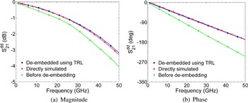
Fig. 11. Comparison of the differential transmission parameter.

Fig. 12. Comparison of the differential to common-mode conversion parameter.

Fig. 13. Comparison of the common-mode transmission parameter.
V. CONCLUSIONS
We have presented the theoretical considerations on the de-embedding of differential devices using the standard cascade-based techniques. In case of a negligible mode conversion on the error networks and on the DUT, the modes can be treated separately and the classical two-port methods, such as TL or TRL can be directly applied on differential S-parameters. However, in case of a negligible mode conversion on the error networks, but non-negligible mode conversion of the DUT, a cascade-based technique has to be applied twice, the results shall be combined into a 4 × 4 matrix and de-embedded from the full DUT matrix. We have verified the presented analysis by measurement of a 2:1 transformer and by simulation of an asymmetrical differential on-chip transmission line.
ACKNOWLEDGEMENTS
The authors would like to thank FhG ENAS, Paderborn, Germany for providing the measurement equipment. We would also like to thank Dr. Werner Simbürger of Infineon Technologies AG, Munich, Germany for the helpful comments. This work was supported under the German BMBF funded project EMCpack/FASMZS 16SV3295.
 Vadim E. Issakov (M'07) was born on August 10, 1981 in The Russian Federation. In 2006 he received the M.Sc. degree (cum laude) in microwave engineering from the Technical University Munich, Germany. In 2010 he received the PhD degree (summa cum laude) from the University of Paderborn, Germany, where he was working as a Research Assistant in the Institute of Electrical Engineering and Information Technology, Department for High-Frequency Electronics from 2006 to 2010. Currently he is with Infineon Technologies AG, Munich, Germany.
His research interests include high frequency, analog and mixed signals circuits in CMOS and Bipolar technology. As well characterization and analytical analysis of passive structures for MMICs, signal integrity problems of interconnects and electromagnetic numerical computations.
 Maciej Wojnowski–received the M.Sc. degree in microwave engineering from the Technical University of Gdansk, Poland, in November 2004. Since March 2005 he works at Infineon Technologies AG, Munich, Germany. His research interests are high-frequency package characterization and wafer-level package integration techniques. He works on calibration and de-embedding techniques for interconnect and passive device characterization for System-in- Package applications. Mr. Wojnowski is co-recipient of the 2007 Outstanding Paper Award of the 9th Electronics Packaging Technology Conference (EPTC 2007).
 Andreas Thiede (IEEE-M'97, SM'99) was born in Berlin in 1961. He received the Dipl.-Ing. and Dr.-Ing. degrees from the Dresden University of Technology in 1986 and 1990, respectively. There he worked on 2-D numerical simulation of GaAs MESFETs and design of GaAs-ICs for high-speed measuring systems.
In 1991 he joined the Fraunhofer-Institute for Applied Solid-State Physics Freiburg and was engaged in the fields of high speed logic, LSI, and mixed signal IC design based on AlGaAs/GaAs quantum well HEMTs. Since 1995 he had been manager of the customer-specific IC's group.
1999 he received a Professorship at University of Paderborn, where he has established the chair for High-Frequency Electronics. Research efforts are focused on integrated high-frequency circuits, currently in particular for high-speed opto-electronic data transmission systems and microwave sensorics.
Andreas Thiede is author and coauthor of more than 100 publications in international journals and conference proceedings, reviewer for several journals and the German Research Foundation, TPC member of the EuMIC symposium, and senior member of the IEEE.
 Robert Weigel was born in Ebermannstadt, Germany, in 1956. He received the Dr.-Ing. and the Dr.-Ing.habil. degrees, both in electrical engineering and computer science, from the Munich University of Technology in Germany, in 1989 and 1992, respectively. From 1982 to 1988, he was a Research Engineer, from 1988 to 1994 a Senior Research Engineer, and from 1994 to 1996 a Professor for RF Circuits and Systems at the Munich University of Technology. In winter 1994/95 he was a Guest Professor for SAW Technology at Vienna University of Technology in Austria. From 1996 to 2002, he has been Director of the Institute for Communications and Information Engineering at the University of Linz, Austria. In August 1999, he co-founded DICE – Danube Integrated Circuit Engineering, Linz, meanwhile an Infineon Technologies Design Center which is devoted to the design of mobile radio circuits and systems. In 2000, he has been appointed a Professor for RF Engineering at the Tongji University in Shanghai, China. Also in 2000, he co-founded the Linz Center of Competence in Mechatronics, meanwhile also a company. Since 2002 he is Head of the Institute for Electronics Engineering at the University of Erlangen-Nuremberg.
He has been engaged in research and development on microwave theory and techniques, integrated optics, high-temperature superconductivity, SAW technology, digital and microwave communication systems, automotive EMC. In these fields, he has published more than 650 papers and given about 300 international presentations. His review work includes international projects and journals. In 2002, he received the German ITG Award, and in 2007 the IEEE Microwave Applications Award. During 2001 to 2003, he has served as a IEEE Distinguished Microwave Lecturer Dr. Weigel is a Fellow of IEEE. He serves on various editorial boards and has been editor of the Proceedings of the European Microwave Association (EuMA). He has been member of numerous conference steering committees. Currently he serves on several company and organization advisory boards. He is an elected scientific advisor of the German research Foundation DFG.


