
1 Introduction
Diodes, or more generally charge transport phenomena, are central to high power microwave sources, vacuum microelectronics, electron and ion sources, and high current drivers used in high-energy density physics experiments. One of the great challenges in these areas is the miniaturization of vacuum and plasma electronic devices. With the combination of recent advances in electronics, photonics and nanotechnology, these miniature devices may integrate with solid-state platforms, thus forming highly compact systems with high power handling capability. Applications in ultrafast electron sources, accelerators, and radiation sources, ranging from millimetre wave to X-rays are envisioned (Booske Reference Booske2008; Barletta et al. Reference Barletta, Bisognano, Corlett, Emma, Huang, Kim, Lindberg, Murphy, Neil and Nguyen2010; Booske et al. Reference Booske, Dobbs, Joye, Kory, Neil, Park, Park and Temkin2011; Peralta et al. Reference Peralta, Soong, England, Colby, Wu, Montazeri, McGuinness, McNeur, Leedle and Walz2013; England et al. Reference England, Noble, Bane, Dowell, Ng, Spencer, Tantawi, Wu, Byer and Peralta2014; Hommelhoff & Kling Reference Hommelhoff and Kling2014; Armstrong Reference Armstrong2015).
Since the pioneering work of Spindt (Spindt Reference Spindt1968; Spindt et al. Reference Spindt, Brodie, Humphrey and Westerberg1976) on the fabrication of cathodes using microfabrication technologies, extensive efforts have been made to scale down vacuum electronic devices to the microscale or even nanoscale. Recently, nanoscale vacuum gap has been used as the conducting channel in nanoelectronics (Srisonphan, Jung & Kim Reference Srisonphan, Jung and Kim2012; Stoner & Glass Reference Stoner and Glass2012; Han & Meyyappan Reference Han and Meyyappan2014; Wu et al. Reference Wu, Wei, Gao, Chen and Peng2016). Because of ballistic transport, vacuum is intrinsically a better carrier transport medium compared to a solid, in which the carriers suffer from optical and acoustic phonon scattering, resulting in local heating and degradation in both signal quality and the device itself. The vacuum-solid-state integrated nanodevices thus combine the advantages of ballistic transport through vacuum with the scalability, low cost and reliability of conventional silicon transistor technology.
This paper highlights some recent modelling efforts in the development of ultrafast and nanoscale diodes, including quantum tunnelling current, ultrafast electron emission, and issues in current crowding and contact resistance. Unsolved problems and challenges in these areas are addressed.
2 Quantum tunnelling current
Tunnelling effects in nanoscale metal-insulator (including vacuum)-metal (MIM) junctions were studied extensively by Simmons in the 1960s (Simmons Reference Simmons1963a ,Reference Simmons b ). Simmons’ formulas were derived by considering only the emission process from the electrodes, where the effects of image charge are considered, but the electron space charge potential and the electron exchange-correlation potential inside the insulator thin films are generally ignored. An excellent review on the tunnelling current in MIM structures is given in Kao (Reference Kao2004). The effects of space charge in a vacuum nanogap have subsequently been studied theoretically (Lau et al. Reference Lau, Chernin, Colombant and Ho1991; Ang, Kwan & Lau Reference Ang, Kwan and Lau2003; Ang & Zhang Reference Ang and Zhang2007) and experimentally (Bhattacharjee, Vartak & Mukherjee Reference Bhattacharjee, Vartak and Mukherjee2008; Bhattacharjee & Chowdhury Reference Bhattacharjee and Chowdhury2009).
Recently, a general scaling law for the quantum tunnelling current in nano- and sub-nanoscale MIM diodes has been developed by self-consistently solving the coupled Schrödinger and Poisson equations (Zhang Reference Zhang2015). It includes the effects of space charge and exchange-correlation potential, as well as current emission from the anode. As shown in figure 1, the self-consistent model recovers various scaling laws in limiting cases: Simmons’s formula (Simmons Reference Simmons1963a ) in the direct tunnelling regime, the Fowler–Nordheim law (Fowler & Nordheim Reference Fowler and Nordheim1928) in the field emission regime, and the quantum Child–Langmuir law (Lau et al. Reference Lau, Chernin, Colombant and Ho1991; Ang et al. Reference Ang, Kwan and Lau2003) in the space charge limited (SCL) regime. Note that in the SCL regime, the self-consistent current approaches the quantum version of the Child–Langmuir law, which exceeds the classical Child–Langmuir law (Child Reference Child1911; Langmuir Reference Langmuir1913) because of quantum tunnelling. Smooth transition between various regimes has been demonstrated.
The proposed model may be applied to broad areas involving tunnelling junctions, for example, quantum plasmonics (Esteban et al. Reference Esteban, Borisov, Nordlander and Aizpurua2012; Savage et al. Reference Savage, Hawkeye, Esteban, Borisov, Aizpurua and Baumberg2012), transition voltage spectroscopy (Trouwborst et al. Reference Trouwborst, Martin, Smit, Guédon, Baart, van der Molen and van Ruitenbeek2011; Bâldea Reference Bâldea2012; Sotthewes et al. Reference Sotthewes, Hellenthal, Kumar and Zandvliet2014), molecular electronics (Bâldea & Köppel Reference Bâldea and Köppel2012; Tan et al. Reference Tan, Wu, Yang, Bai, Bosman and Nijhuis2014), and resistive switching (Ziegler, Harnack & Kohlstedt Reference Ziegler, Harnack and Kohlstedt2014).
Further studies on quantum tunnelling current may include: (i) examination of the Wentzel–Kramers–Brillouin–Jeffreys (WKBJ) approximation and the free electron gas model assumed for the electrodes against exact first principle calculations (Zhang, Lu & Pantelides Reference Zhang, Lu and Pantelides2006; Yaghoobi, Walus & Nojeh Reference Yaghoobi, Walus and Nojeh2009); (ii) the effects of electrode geometry (Luginsland, Lau & Gilgenbach Reference Luginsland, Lau and Gilgenbach1996; Lau Reference Lau2001; Luginsland et al. Reference Luginsland, Lau, Umstattd and Watrous2002; Rokhlenko & Lebowitz Reference Rokhlenko and Lebowitz2003; Shiffler et al. Reference Shiffler, Statum, Hussey, Zhou and Mardahl2005; Jensen Reference Jensen2010; Tang et al. Reference Tang, Shiffler, Golby, LaCour and Knowles2012; Fairchild et al. Reference Fairchild, Boeckl, Back, Ferguson, Koerner, Murray, Maruyama, Lange, Cahay and Behabtu2015; Harris et al. Reference Harris, Jensen, Shiffler and Petillo2015; Jensen et al. Reference Jensen, Shiffler, Rittersdorf, Lebowitz, Harris, Lau, Petillo, Tang and Luginsland2015); (iii) comparison of the classical image charge potential with that of quantum theory (Newns Reference Newns1969; Koh & Ang Reference Koh and Ang2008; Myöhänen et al. Reference Myöhänen, Tuovinen, Korhonen, Stefanucci and van Leeuwen2012); (iv) the nature of the ion lattice of the electrodes (Spindt et al. Reference Spindt, Brodie, Humphrey and Westerberg1976); (v) dissimilar electrode materials (Simmons Reference Simmons1963b ); (vi) possible charge trapping inside the insulator film (Rose Reference Rose1955; Kao Reference Kao2004); (vii) ac bias and time/frequency dependence (Valfells et al. Reference Valfells, Feldman, Virgo, O’Shea and Lau2002; Feng & Verboncoeur Reference Feng and Verboncoeur2005, Reference Feng and Verboncoeur2006, Reference Feng and Verboncoeur2008; Pedersen, Manolescu and Valfells Reference Pedersen, Manolescu and Valfells2010; Caflisch & Rosin Reference Caflisch and Rosin2012; Cocker et al. Reference Cocker, Jelic, Gupta, Molesky, Burgess, Reyes, Titova, Tsui, Freeman and Hegmann2013; Griswold, Fisch & Wurtele Reference Griswold, Fisch and Wurtele2012; Rokhlenko Reference Rokhlenko2015; Liu et al. Reference Liu, Zhang, Chen and Ang2015a ,Reference Liu, Zhang, Chen and Ang b ; Griswold & Fisch Reference Griswold and Fisch2016); and (viii) comparison of theory and modelling with experiments (Spindt et al. Reference Spindt, Brodie, Humphrey and Westerberg1976; Das & Jagadeesh Reference Das and Jagadeesh1981; Teague Reference Teague1986; Cahay et al. Reference Cahay, McLennan, Datta and Lundstrom1987; Bhattacharjee et al. Reference Bhattacharjee, Vartak and Mukherjee2008; Bhattacharjee & Chowdhury Reference Bhattacharjee and Chowdhury2009; Bormann et al. Reference Bormann, Gulde, Weismann, Yalunin and Ropers2010; Cocker et al. Reference Cocker, Jelic, Gupta, Molesky, Burgess, Reyes, Titova, Tsui, Freeman and Hegmann2013; Tan et al. Reference Tan, Wu, Yang, Bai, Bosman and Nijhuis2014). These studies are important to vacuum nanoelectronics, including gated vacuum nanodevices (Han, Oh & Meyyappan Reference Han, Oh and Meyyappan2012), transition voltage spectroscopy in vacuum diodes (Bâldea Reference Bâldea2014) and non-equilibrium vacuum tunnelling junctions (Maksymovych Reference Maksymovych2013).

Figure 1. Self-consistent model for the quantum tunnelling current in a one-dimensional planar nanoscale Au-vaccum-Au diode (Zhang Reference Zhang2015). The gap distance is
 $D=1~\text{nm}$
, gap voltage is
$D=1~\text{nm}$
, gap voltage is
 $V_{g}$
and the normalized current density
$V_{g}$
and the normalized current density
 $\unicode[STIX]{x1D6FE}=J/J_{CL}$
is in terms of the Child–Langmuir law
$\unicode[STIX]{x1D6FE}=J/J_{CL}$
is in terms of the Child–Langmuir law
 $J_{CL}$
. The
$J_{CL}$
. The
 $J$
-V (current density–voltage) curve is compared with scaling laws in various limits: Simmons formula (Simmons Reference Simmons1963a
), Fowler–Nordheim (FN) law (Fowler & Nordheim Reference Fowler and Nordheim1928), Child–Langmuir (CL) law (Child Reference Child1911; Langmuir Reference Langmuir1913) and quantum CL law (Lau et al.
Reference Lau, Chernin, Colombant and Ho1991; Ang et al.
Reference Ang, Kwan and Lau2003).
$J$
-V (current density–voltage) curve is compared with scaling laws in various limits: Simmons formula (Simmons Reference Simmons1963a
), Fowler–Nordheim (FN) law (Fowler & Nordheim Reference Fowler and Nordheim1928), Child–Langmuir (CL) law (Child Reference Child1911; Langmuir Reference Langmuir1913) and quantum CL law (Lau et al.
Reference Lau, Chernin, Colombant and Ho1991; Ang et al.
Reference Ang, Kwan and Lau2003).
3 Ultrafast electron emission
Laser-driven ultrafast electron emission offers the possibility of manipulation and control of coherent electron dynamics in ultrashort spatio-temporal scales (Hommelhoff & Kling Reference Hommelhoff and Kling2014). Production of ultrashort electron bunches provides the enabling technology for four-dimensional (4-D) time-resolved electron microscopy (Tao et al. Reference Tao, Zhang, Duxbury, Berz and Ruan2012; Portman et al. Reference Portman, Zhang, Tao, Makino, Berz, Duxbury and Ruan2013). It is also important to free electron lasers, laser acceleration of relativistic electrons, and ultrafast electron diffraction (Hommelhoff, Kealhofer & Kasevich Reference Hommelhoff, Kealhofer and Kasevich2006; Ropers et al. Reference Ropers, Solli, Schulz, Lienau and Elsaesser2007). Perturbative theory to model laser-driven ultrafast electron emission was usually done with the strong field approximation (Bormann et al. Reference Bormann, Gulde, Weismann, Yalunin and Ropers2010). Existing Floquet models for electron emission include only a laser wave field with zero direct current (dc) bias (Yalunin, Gulde & Ropers Reference Yalunin, Gulde and Ropers2011).
We constructed an analytic solution for the highly nonlinear electron emission from a metal surface that is exposed to both a dc biased electric field and a single frequency laser electric field (Zhang & Lau Reference Zhang and Lau2016). By solving the time-dependent Schrödinger equation exactly, our theory is valid for arbitrary laser frequency and metal properties (work function and Fermi level). Various emission mechanisms, including multiphoton absorption or emission, optical or dc field emission, single-photon induced over-barrier emission, and various combinations of these, are all included in a single formulation. The time-dependent emission current reveals that intense current modulation may be possible even with a low intensity laser, by only increasing the applied dc bias, as shown in figure 2. A slowly varying envelope approximation has extended the results to pulsed excitation (Zhang & Lau Reference Zhang and Lau2016).

Figure 2. Time-dependent total emission current density
 $w$
(
$w$
(
 $x$
,
$x$
,
 $t$
) normalized to the time-averaged emission current density
$t$
) normalized to the time-averaged emission current density
 ${<}w>$
, as a function of time
${<}w>$
, as a function of time
 $t$
and space
$t$
and space
 $x$
, for laser electric field
$x$
, for laser electric field
 $F_{\text{1}}=1~\text{V}~\text{nm}^{-1}$
under three dc fields
$F_{\text{1}}=1~\text{V}~\text{nm}^{-1}$
under three dc fields
 $F_{0}=1,5,10~\text{V}~\text{nm}^{-1}$
(Zhang & Lau Reference Zhang and Lau2016). Time is normalized to the laser period
$F_{0}=1,5,10~\text{V}~\text{nm}^{-1}$
(Zhang & Lau Reference Zhang and Lau2016). Time is normalized to the laser period
 $2\unicode[STIX]{x03C0}/\unicode[STIX]{x1D714}$
, and space is normalized to a length scale
$2\unicode[STIX]{x03C0}/\unicode[STIX]{x1D714}$
, and space is normalized to a length scale
 $\sqrt{\hslash ^{2}/2mW}$
, where
$\sqrt{\hslash ^{2}/2mW}$
, where
 $\unicode[STIX]{x1D714}$
is the laser frequency,
$\unicode[STIX]{x1D714}$
is the laser frequency,
 $m$
is the electron rest mass and
$m$
is the electron rest mass and
 $W$
is the metal work function. We assumed the metal is gold, with
$W$
is the metal work function. We assumed the metal is gold, with
 $W=5.1~\text{eV}$
, Fermi level
$W=5.1~\text{eV}$
, Fermi level
 $E_{F}=5.53~\text{eV}$
and laser wavelength
$E_{F}=5.53~\text{eV}$
and laser wavelength
 $\unicode[STIX]{x1D706}=800~\text{nm}$
. The vacuum–metal interface is located at
$\unicode[STIX]{x1D706}=800~\text{nm}$
. The vacuum–metal interface is located at
 $x=0$
.
$x=0$
.
Future studies on ultrafast electron emission may include emission delay and scattered electron contributions, charge redistribution and thermalization (Pant & Ang Reference Pant and Ang2013), field enhancement (Feng & Verboncoeur Reference Feng and Verboncoeur2005, Reference Feng and Verboncoeur2006, Reference Feng and Verboncoeur2008; Miller, Lau & Booske Reference Miller, Lau and Booske2007; Feng, Verboncoeur & Lin Reference Feng, Verboncoeur and Lin2008; Jensen et al. Reference Jensen, Lau, Feldman and O’Shea2008; Tang, Shiffler & Cartwright Reference Tang, Shiffler and Cartwright2011) and space charge effects (Griswold, Fisch & Wurtele Reference Griswold, Fisch and Wurtele2010; Pedersen et al. Reference Pedersen, Manolescu and Valfells2010; Caflisch & Rosin Reference Caflisch and Rosin2012; Griswold et al. Reference Griswold, Fisch and Wurtele2012; Ilkov et al. Reference Ilkov, Torfason, Manolescu and Valfells2015; Rokhlenko Reference Rokhlenko2015; Liu et al. Reference Liu, Zhang, Chen and Ang2015a ,Reference Liu, Zhang, Chen and Ang b ; Griswold & Fisch Reference Griswold and Fisch2016), all under ultrafast conditions. It is important to link ultrafast strong-field laser physics in atoms and gaseous media to that in nanoclusters, solid-state surfaces and nanostructures (Corkum et al. Reference Corkum, Brunel, Sherman and Srinivasan-Rao1988; Corkum Reference Corkum1993; Corkum, Burnett & Ivanov Reference Corkum, Burnett and Ivanov1994; Rundquist et al. Reference Rundquist, Durfee, Chang, Herne, Backus, Murnane and Kapteyn1998; Corkum & Krausz Reference Corkum and Krausz2007; Fan et al. Reference Fan, Grychtol, Knut, Hernández-García, Hickstein, Zusin, Gentry, Dollar, Mancuso and Hogle2015; Chen et al. Reference Chen, Tao, Hernández-García, Matyba, Carr, Knut, Kfir, Zusin, Gentry and Grychtol2016; Tao et al. Reference Tao, Chen, Szilvási, Keller, Mavrikakis, Kapteyn and Murnane2016). These studies would offer unprecedented scientific advances in attosecond science (Corkum & Krausz Reference Corkum and Krausz2007; Hommelhoff & Kling Reference Hommelhoff and Kling2014; Tao et al. Reference Tao, Chen, Szilvási, Keller, Mavrikakis, Kapteyn and Murnane2016).
4 Current crowding and contact resistance
Contact resistance and current crowding are very important to plasma and vacuum electronics, such as wire array
 $z$
-pinches (Gomez et al.
Reference Gomez, Zier, Gilgenbach, French, Tang and Lau2008; Zier et al.
Reference Zier, Gomez, French, Gilgenbach, Lau, Tang, Cuneo, Mehlhorn, Johnston and Mazarakis2008), field emitters (Shiffler et al.
Reference Shiffler, Statum, Hussey, Zhou and Mardahl2005; Park et al.
Reference Park, Cola, Siegmund, Xu, Maschmann, Fisher and Kim2006; Vlahos, Booske & Morgan Reference Vlahos, Booske and Morgan2007) and high power microwave devices (Booske Reference Booske2008; Benford, Swegle & Schamiloglu Reference Benford, Swegle and Schamiloglu2015). In these systems, poor electrical contact prevents efficient power coupling to the load, produces unwanted plasma and even damages the electrodes. Contact resistance is also extremely important in wafer evaluation (Carbonero, Morin & Cabon Reference Carbonero, Morin and Cabon1995), thin film resistors (Hall Reference Hall1968) and metal-oxide–vacuum junctions (Latham Reference Latham1995). It is critical to semiconductor material and device characterization (Berger Reference Berger1972; Schroder Reference Schroder1998). Contact resistance is one of the major limiting factors to devices made of exceptional materials, such as carbon nanotubes (CNTs), graphene and diamond (Li, Thostenson & Chou Reference Li, Thostenson and Chou2007; Grotjohn et al.
Reference Grotjohn, Tran, Yaran, Demlow and Schuelke2014; Nouchi & Tanigaki Reference Nouchi and Tanigaki2014).
$z$
-pinches (Gomez et al.
Reference Gomez, Zier, Gilgenbach, French, Tang and Lau2008; Zier et al.
Reference Zier, Gomez, French, Gilgenbach, Lau, Tang, Cuneo, Mehlhorn, Johnston and Mazarakis2008), field emitters (Shiffler et al.
Reference Shiffler, Statum, Hussey, Zhou and Mardahl2005; Park et al.
Reference Park, Cola, Siegmund, Xu, Maschmann, Fisher and Kim2006; Vlahos, Booske & Morgan Reference Vlahos, Booske and Morgan2007) and high power microwave devices (Booske Reference Booske2008; Benford, Swegle & Schamiloglu Reference Benford, Swegle and Schamiloglu2015). In these systems, poor electrical contact prevents efficient power coupling to the load, produces unwanted plasma and even damages the electrodes. Contact resistance is also extremely important in wafer evaluation (Carbonero, Morin & Cabon Reference Carbonero, Morin and Cabon1995), thin film resistors (Hall Reference Hall1968) and metal-oxide–vacuum junctions (Latham Reference Latham1995). It is critical to semiconductor material and device characterization (Berger Reference Berger1972; Schroder Reference Schroder1998). Contact resistance is one of the major limiting factors to devices made of exceptional materials, such as carbon nanotubes (CNTs), graphene and diamond (Li, Thostenson & Chou Reference Li, Thostenson and Chou2007; Grotjohn et al.
Reference Grotjohn, Tran, Yaran, Demlow and Schuelke2014; Nouchi & Tanigaki Reference Nouchi and Tanigaki2014).
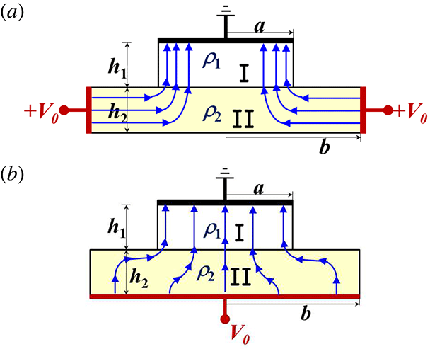
The fundamental model of electrical contact, Holm’s
 $a$
-spot theory (Holm Reference Holm1967; Schroder Reference Schroder1998; Timsit Reference Timsit1999; Chin, Barber & Hu Reference Chin, Barber and Hu2006), is generalized to include the effects of dissimilar materials and higher dimensions (Gomez et al.
Reference Gomez, French, Tang, Zhang, Lau and Gilgenbach2009; Lau & Tang Reference Lau and Tang2009; Zhang & Lau Reference Zhang and Lau2010; Zhang Reference Zhang2012). By using Fourier series analysis, we derived new, simple analytical scaling laws for the total resistance for arbitrary values of dimensions and resistivities, for both Cartesian and cylindrical geometries (Zhang & Lau Reference Zhang and Lau2010). The models are extended to thin film contacts for two basic configurations: the horizontal type (figure 3
a) (Zhang, Lau & Gilgenbach Reference Zhang, Lau and Gilgenbach2011; Zhang, Lau & Timsit Reference Zhang, Lau and Timsit2012; Zhang, Hung & Lau Reference Zhang, Hung and Lau2013; Zhang & Lau Reference Zhang and Lau2014) and the vertical type (figure 3
b) (Zhang & Lau Reference Zhang and Lau2013). Current crowding is systematically studied by calculating the current flow patterns (Zhang, Lau & Gilgenbach Reference Zhang, Lau and Gilgenbach2015a
). The exact field solution accounts for both interface resistance and spreading resistance. It was recently applied to study current crowding and constriction resistance in electrically pumped nanolasers, where the effects of sidewall tilt were analysed (Zhang et al.
Reference Zhang, Gu, Lau and Fainman2016).
$a$
-spot theory (Holm Reference Holm1967; Schroder Reference Schroder1998; Timsit Reference Timsit1999; Chin, Barber & Hu Reference Chin, Barber and Hu2006), is generalized to include the effects of dissimilar materials and higher dimensions (Gomez et al.
Reference Gomez, French, Tang, Zhang, Lau and Gilgenbach2009; Lau & Tang Reference Lau and Tang2009; Zhang & Lau Reference Zhang and Lau2010; Zhang Reference Zhang2012). By using Fourier series analysis, we derived new, simple analytical scaling laws for the total resistance for arbitrary values of dimensions and resistivities, for both Cartesian and cylindrical geometries (Zhang & Lau Reference Zhang and Lau2010). The models are extended to thin film contacts for two basic configurations: the horizontal type (figure 3
a) (Zhang, Lau & Gilgenbach Reference Zhang, Lau and Gilgenbach2011; Zhang, Lau & Timsit Reference Zhang, Lau and Timsit2012; Zhang, Hung & Lau Reference Zhang, Hung and Lau2013; Zhang & Lau Reference Zhang and Lau2014) and the vertical type (figure 3
b) (Zhang & Lau Reference Zhang and Lau2013). Current crowding is systematically studied by calculating the current flow patterns (Zhang, Lau & Gilgenbach Reference Zhang, Lau and Gilgenbach2015a
). The exact field solution accounts for both interface resistance and spreading resistance. It was recently applied to study current crowding and constriction resistance in electrically pumped nanolasers, where the effects of sidewall tilt were analysed (Zhang et al.
Reference Zhang, Gu, Lau and Fainman2016).

Figure 3. Two basic types of thin film contact: (a) the horizontal type (Zhang et al. Reference Zhang, Lau and Gilgenbach2011, Reference Zhang, Lau and Timsit2012, Reference Zhang, Hung and Lau2013; Zhang & Lau Reference Zhang and Lau2014) and (b) the vertical type (Zhang & Lau Reference Zhang and Lau2013).
When electrical contacts are formed in micro- or nanoscale, the electron mean free path
 $l$
may exceed the contact size
$l$
may exceed the contact size
 $a$
, so that electrons transport ballistically through the contact constriction (Sharvin Reference Sharvin1965; Landauer Reference Landauer1996; Zhang & Hung Reference Zhang and Hung2014). If the system size is further reduced to be of the order of the Fermi wavelength, wave character features would be pronounced, where the quantization of ballistic electron transport through a constriction represents conduction as transmission. There are existing models of electrical contacts in ballistic (Sharvin Reference Sharvin1965; Büttiker Reference Büttiker1988; Datta & Anantram Reference Datta and Anantram1992; Landauer Reference Landauer1996) and quantum regimes (Mortensen et al.
Reference Mortensen, Johnsen, Jauho and Flensberg1999; Datta Reference Datta2005; Grosse et al.
Reference Grosse, Bae, Lian, Pop and King2011; Solomon Reference Solomon2011; Xia et al.
Reference Xia, Perebeinos, Lin, Wu and Avouris2011). However, the transition between the classical, ballistic and quantum regimes remains unclear, and it requires further investigation. The underlying physics in these regimes is critical to the design and performance of the multitude of new devices that are expected to be developed in the near future.
$a$
, so that electrons transport ballistically through the contact constriction (Sharvin Reference Sharvin1965; Landauer Reference Landauer1996; Zhang & Hung Reference Zhang and Hung2014). If the system size is further reduced to be of the order of the Fermi wavelength, wave character features would be pronounced, where the quantization of ballistic electron transport through a constriction represents conduction as transmission. There are existing models of electrical contacts in ballistic (Sharvin Reference Sharvin1965; Büttiker Reference Büttiker1988; Datta & Anantram Reference Datta and Anantram1992; Landauer Reference Landauer1996) and quantum regimes (Mortensen et al.
Reference Mortensen, Johnsen, Jauho and Flensberg1999; Datta Reference Datta2005; Grosse et al.
Reference Grosse, Bae, Lian, Pop and King2011; Solomon Reference Solomon2011; Xia et al.
Reference Xia, Perebeinos, Lin, Wu and Avouris2011). However, the transition between the classical, ballistic and quantum regimes remains unclear, and it requires further investigation. The underlying physics in these regimes is critical to the design and performance of the multitude of new devices that are expected to be developed in the near future.
5 Concluding remarks
Ultrafast and nanoscale diodes are essential components in the miniaturization of plasma and vacuum electronics, as recognized in a recent white paper for the US Department of Energy (Zhang et al. Reference Zhang, Luginsland, Lau, Booske, Gilgenbach, Jensen, Peckerar, Shiffler, Fairchild and Verboncoeur2015b ). Here, we review recent modelling efforts on three aspects of nanoscale diodes, quantum tunnelling, ultrafast electron emission and electrical contact. Unsolved problems and challenges in these areas are addressed.
The research outlined above is pushing the traditional boundary of plasma science and engineering, into neighbouring fields of nanoelectronics, ultrafast physics and material science. The applications of these research are immense, including single-molecule sensing, transition voltage spectroscopy, molecule electronics, resistive switching, CNT-, graphene- and diamond-based electronics, novel high brightness electron sources, ultrafast electron microscopes, variable stoichiometry photoemissive materials for detectors and sources, and novel compact particle accelerators.
Acknowledgements
This work was supported by AFOSR grant no. FA9550-14-1-0309. P.Z. was also supported by AFOSR through a subcontract from the University of Michigan.