


Introduction
Microwave filters with high performance, compact size, low loss, and low cost are required due to advancements in wireless communication systems. Substrate-integrated waveguide (SIW) is a promising solution for designing microwave filters with high performance. SIW has the advantages of low loss, low cost, easy fabrication, and easy integration with planar circuits [Reference Deslandes and Wu1]. Transmission zeros (TZs) are created at finite frequencies to improve the frequency selectivity of microwave filters. Cross-coupling, source-load coupling, non-resonating nodes, triplet schemes, and non-resonating modes are widely used to create TZs, where only electric or magnetic coupling exists between two adjacent resonators [Reference Chen, Hong, Cui, Hao and Wu2–Reference Tomassoni, Silvestri, Bozzi and Perregrini12]. Recently, mixed electric and magnetic coupling is adopted to build dual-coupling paths between two adjacent resonators, which lead to signal cancellation effects and create TZs, whose location can be controlled by adjusting the mixed coupling coefficients [Reference Chu and Wang13–Reference Li, You, Yu and He19]. Second-order filters have been presented to produce one TZ below or above the passband using mixed coupling [Reference Chu and Wang13, Reference Gong, Hong, Zhang, Chen and You14]. Inter-digital slot-lines are combined with an iris-window to create mixed coupling between two resonators [Reference Shen, Wu, Sun, Yin and Mao15]. A hybrid structure of SIW and coplanar waveguide is presented to produce mixed coupling for the generation of TZs [Reference Chu, Hong, Dai, Tang, Chen, Hao, Zhu and Wu16]. A multilayer SIW filter with mixed coupled trisections is designed to improve stopband performance [Reference Xu, Wang, Liao and Shi17]. A multiple-layer structure with two types of cross-coupled units with different cross-coupling signs is used to design a bandpass filter with two TZs below and above the passband [Reference Wong, Chen, Lin, Zhu and Chu18]. A substrate-integrated folded waveguide controllable mixed electric and magnetic coupling structure is proposed for millimeter-wave filter applications [Reference Li, You, Yu and He19]. Most of the reported SIW structures with mixed coupling are implemented on multilayer substrate [Reference Gong, Hong, Zhang, Chen and You14, Reference Xu, Wang, Liao and Shi17–Reference Li, You, Yu and He19]. In comparison to multilayer structures, single-layer SIW structures have the advantages of low cost and easy fabrication. Mixed coupling structures implemented on a single-layer substrate have been reported [Reference Shen, Wu, Sun, Yin and Mao15, Reference Chu, Hong, Dai, Tang, Chen, Hao, Zhu and Wu16] and the achieved fractional bandwidth is 6% in [Reference Shen, Wu, Sun, Yin and Mao15] and 7% in [Reference Chu, Hong, Dai, Tang, Chen, Hao, Zhu and Wu16] (filter III), to the best of authors’ knowledge. In addition, most of the reported mixed coupling structures implemented on a single-layer SIW do not present a detailed analysis of the coupling structure, such as available range of coupling coefficient, realizable bandwidth, and how to control the location of TZ and the electric and magnetic coupling separately.
This paper presents a planar SIW structure with mixed electric and magnetic coupling implemented on a single-layer substrate. Three slot-lines on the top metal plane are combined with a conventional iris-window between two cavities to produce mixed coupling. The electric and magnetic coupling can be separately controlled by adjusting the dimensions of the slot-lines and the width of the iris-window. It has been shown that a TZ can be created in a second-order filter with mixed coupling, and the TZ can be positioned below or above the passband corresponding to dominant magnetic or dominant electric coupling, respectively, which is similar to the discussion presented in [Reference Chu and Wang13, Reference Gong, Hong, Zhang, Chen and You14]. Moreover, the filter bandwidth can be controlled by adjusting the electric and magnetic coupling coefficients. In addition, the proposed coupling structure provides a wide range of coupling intensities, which can be used to design highly selective filters with narrow, moderate, and wide bandwidths. Third- and fourth-order cross-coupled generalized Chebyshev bandpass filters operating in X-band are designed, fabricated, and measured to validate the proposed structure. The third- and fourth-order filters are centered at 10.07 and 10.13 GHz with a 1 dB fractional bandwidth of 8.9 and 10.8%, respectively. The comparisons between simulated and measured results are provided, which show that they are in good agreement.
Proposed mixed coupling structure
The proposed structure with mixed electric and magnetic coupling is shown in Fig. 1. The structure is designed on Rogers RT Duroid 5880 with dielectric permittivity ε r = 2.2, substrate thickness h = 0.787 mm, and loss tangent tanδ = 0.0009 (at 10 GHz). The metalized via-holes have a diameter of d = 0.6 mm and a center-to-center spacing between two adjacent via-holes p = 1 mm. The mixed coupling structure is implemented by etching three slot-lines on the top metal plane and introducing an iris-window between two cavities. Electric coupling can be controlled by adjusting the dimensions of the slot-lines, whereas magnetic coupling depends on the width of the iris-window. Therefore, the coexistent electric and magnetic coupling between the two cavities creates the mixed coupling.
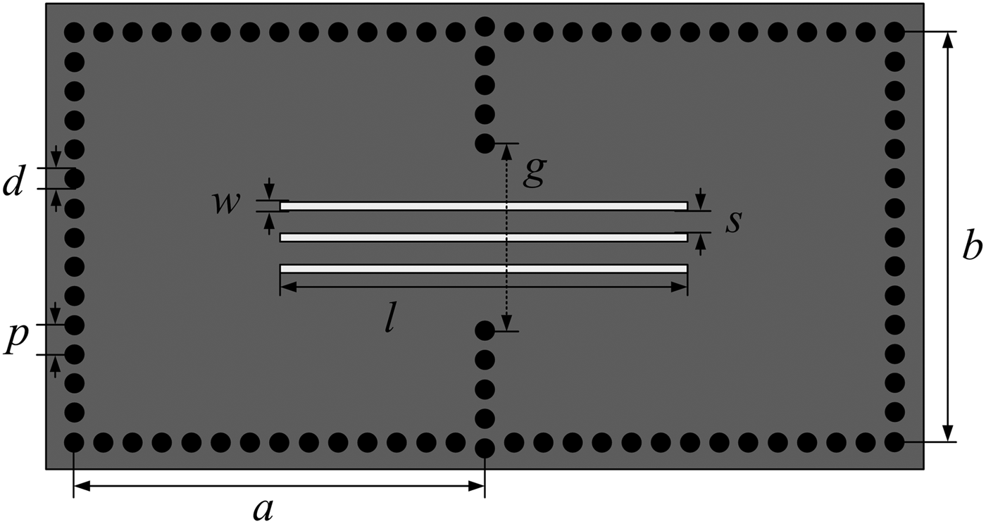
Fig. 1. Proposed mixed electric and magnetic coupling structure.
A two-coupled cavity model (based on Fig. 1) was simulated to analyze the mixed coupling structure. The simulations were performed using full-wave simulator Ansys HFSS. The initial dimensions of TE101-mode-based SIW cavity can be determined by using the relations [Reference Cassivi, Perregrini, Arcioni, Bressan, Wu and Conciauro20].
 $$f_0 = \displaystyle{{c_0} \over {2\sqrt {\varepsilon _r}}} \sqrt {\displaystyle{1 \over {a_{eff} ^2}} + \displaystyle{1 \over {b_{eff} ^2}}}, $$
where
 $$a_{eff} = a - \displaystyle{{d^2} \over {0.95p}},\quad b_{eff} = b - \displaystyle{{d^2} \over {0.95p}}.$$
Here, a and b are the length and width of the TE101-mode-based SIW cavity, respectively, and c 0 is the velocity of light in vacuum. The simulated electric field vectors of the first two modes of the proposed mixed coupling structure are shown in Figs 2 and 3. The values of the parameters in the simulation are: a = 14 mm and b = 14.5 mm. When l = 14 mm, w = 0.3 mm, s = 0.4 mm, and g = 5 mm, the E-field of the first resonant mode is 1800 out-phase in the two adjacent cavity resonators, while the E-field of the second resonant mode is in-phase for the two adjacent cavity resonators, as shown in Fig. 2. It indicates that the electric coupling is dominant between the two resonators. When l = 14 mm, w = 0.2 mm, s = 0.3 mm, and g = 7.5 mm, the E-field of the first resonant mode is in-phase for the two adjacent cavity resonators, while the E-field of the second resonant mode is 1800 out-phase in the two adjacent cavity resonators, as shown in Fig. 3. This indicates that the magnetic coupling is dominant between the two resonators. Therefore, it can be concluded that the proposed structure realizes mixed coupling with dominant electric or magnetic coupling.

Fig. 2. E-field of the proposed mixed coupling structure with dominant electric coupling: (a) first resonant mode; (b) second resonant mode.

Fig. 3. E-field of the proposed mixed coupling structure with dominant magnetic coupling: (a) first resonant mode; (b) second resonant mode.
The coupling coefficient can be extracted using the following formula [Reference Hong and Lancaster21]:
 $$k = \displaystyle{{\omega _{odd}^2 - \omega _{even}^2} \over {\omega _{odd}^2 + \omega _{even}^2}}, $$
where ω odd and ω even are the odd-mode and even-mode resonant frequencies, respectively, and k is the coupling coefficient between the two resonators. The odd-mode has a lower resonant frequency than the even-mode, as shown in Fig. 2, which indicates that k < 0. The even-mode has a lower resonant frequency than the odd-mode, as shown in Fig. 3, which indicates that k > 0. The conditions k < 0 and k > 0 stand for the electric coupling is dominant and magnetic coupling is dominant, respectively.
The coupling coefficient of the proposed coupling structure against l, w, s, and g are presented in Fig. 4. The coexistence of electric and magnetic coupling was observed. The coupling coefficient and the dominance of coupling (electric or magnetic) can be controlled by adjusting the parameters l, w, s, and g. The initial values of the parameters in the simulation are: a = 14 mm and b = 14.5 mm. When the values of the parameters are: w = 0.25 mm, s = 0.4 mm, g = 5 mm, and l is varied from 11 to 16 mm, it can be observed that the electric coupling is dominant and the coupling coefficient decreases with increase in l, as shown in Fig. 4(a). When l = 15 mm, s = 0.4 mm, and g = 6 mm, it has been seen that the coupling coefficient decreases until it changes from magnetic to electric and then increases again as w increases from 0.1 to 0.5 mm, as presented in Fig. 4(b). It was observed that the dominance of coupling changes from magnetic to electric when l = 15 mm, w = 0.2 mm, g = 6 mm, and the variable s varies from 0.1 to 0.6 mm, as shown in Fig. 4(c). When the values of the parameters are: l = 14 mm, w = 0.4 mm, s = 0.4 mm, and g is increased from 4 to 12 mm, it can be observed that the coupling coefficient decreases until it changes from electric to magnetic and then increases again as g increases, as shown in Fig. 4(d). It can be seen that the electric and magnetic coupling can be controlled by adjusting the dimensions of the slot-lines and the width of the iris-window. Moreover, the proposed mixed coupling structure exhibits a wide range of coupling strength from −0.075 to 0.08, which can be used to design a filter with narrow, moderate, and wide band performance.

Fig. 4. Coupling coefficient of the proposed mixed coupling structure against: (a) l; (b) w; (c) s; (d) g.
Second-order filter with mixed coupling
The configuration of the second-order filter using the proposed mixed electric and magnetic coupling structure is shown in Fig. 5. The filter is excited with the 50 Ω microstrip lines with coupling slots as its input and output feed lines. The equivalent circuit of the second-order filter with mixed coupling is shown in Fig. 6, as described in [Reference Gong, Hong, Zhang, Chen and You14]. Each resonator can be characterized by a parallel capacitance C together with an inductance L. Its resonant frequency is equal to ω 0 = (LC)−1/2. C m and L m represent the coupling capacitance and inductance, and they produce electric and magnetic coupling, respectively. C m can be controlled by adjusting the dimensions of the slot-lines and L m depends on the width of the iris-window, as discussed in the last section.
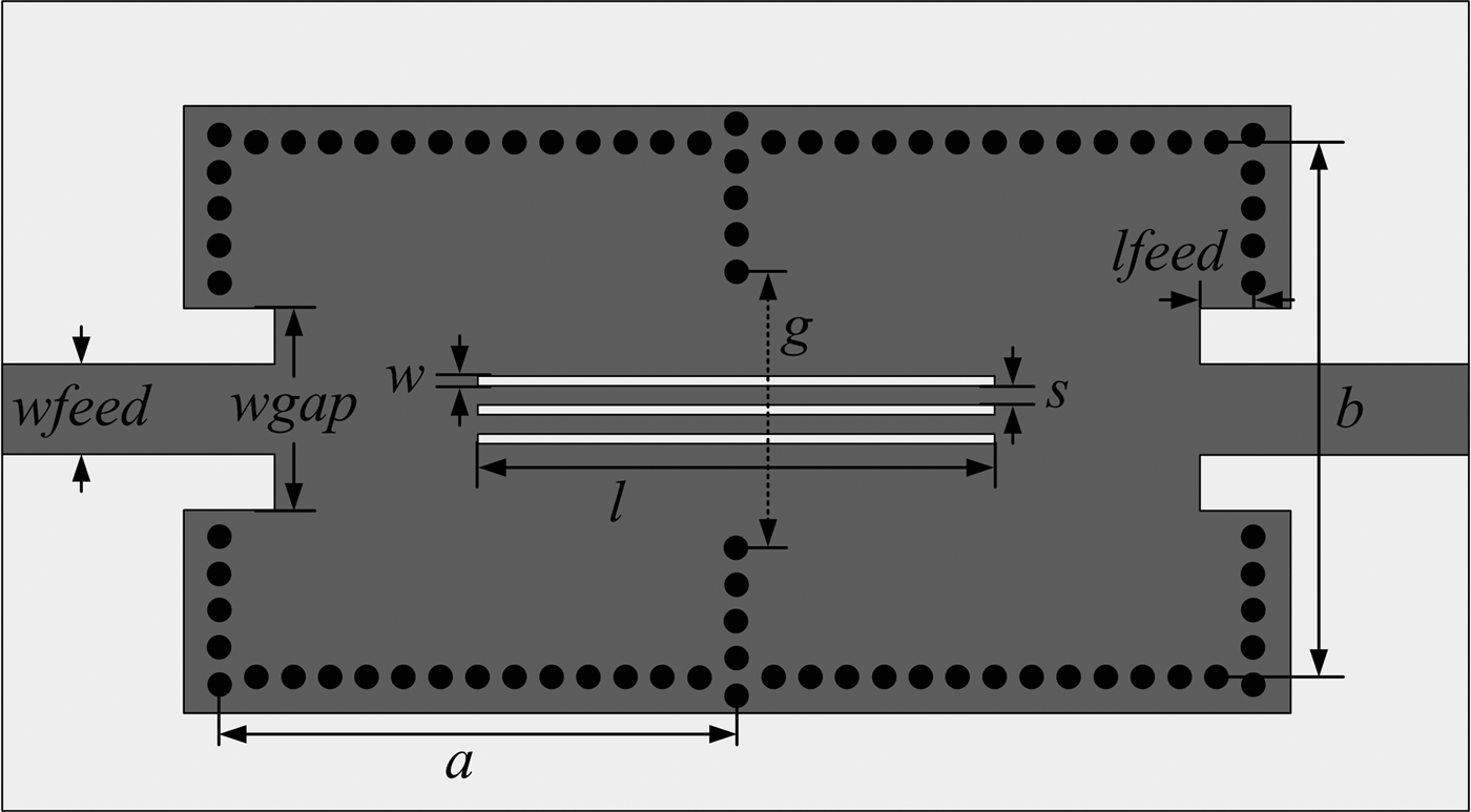
Fig. 5. Configuration of the second-order filter with mixed coupling (the initial values of the parameters in the simulation are as follows: a = 14 mm, b = 14.5 mm, wfeed = 2.43 mm, wgap = 5 mm, and lfeed = 1 mm).

Fig. 6. Equivalent circuit of the second-order filter with mixed coupling.
The total mixed coupling coefficient can also be obtained by using the relation [Reference Chu and Wang13]:
 $$k = \displaystyle{{M_C - E_C} \over {1 - M_C E_C}}, $$
 $$M_C = \displaystyle{{L_m} \over L} = \displaystyle{1 \over 2}\left[ {\displaystyle{{\omega _{odd}^2 - \omega _0^2} \over {\omega _{odd}^2 - \omega _m^2}} + \displaystyle{{\omega _{even}^2 - \omega _0^2} \over {\omega _m^2 - \omega _{even}^2}}} \right],$$
 $$E_C = \displaystyle{C \over {C_m}} = \displaystyle{{\omega _m^2} \over {2\omega _0^2}} \left[ {\displaystyle{{\omega _0^2 - \omega _{odd}^2} \over {\omega _m^2 - \omega _{odd}^2}} + \displaystyle{{\omega _0^2 - \omega _{even}^2} \over {\omega _{even}^2 - \omega _m^2}}} \right].$$
where M C is the magnetic coupling coefficient and E C is the electric coupling coefficient. From relations (4), (5), and (6), it can be observed that the total mixed coupling coefficient k is determined by both M C and E C simultaneously, and it can be easily changed by adjusting L m and C m. The second-order filter with mixed coupling will create a TZ characterized by ω m = (L mCm)−1/2, and it has a relationship with ω 0 as follows [Reference Chu and Wang13, Reference Gong, Hong, Zhang, Chen and You14]:
 $$\displaystyle{{\omega _0} \over {\omega _m}} = \sqrt {\displaystyle{{M_C} \over {E_C}}}. $$
According to the relations (4) and (7), when M C > E C (k > 0), the magnetic coupling is dominant and the TZ will be located below the passband, while the electric coupling is dominant and the TZ will be located above the passband when M C < E C (k < 0). The simulated S 21-parameters of the second-order filter with mixed electric and magnetic coupling against the variation in the parameters l, w, s, and g are presented in Fig. 7. It can be seen that a TZ is created by introducing the mixed coupling between two adjacent cavities. The TZ is located above the passband when M C < E C, and the TZ appears below the passband when M C > E C. It can also be observed that the TZ moves right with the decrease of M C/E C, and moves left when M C/E C increases. In all cases, it can be seen that the bandwidth of the filter increases if |M C−E C| increases. By analyzing the results presented in Fig. 7, it can be concluded that the location of the TZ and the bandwidth of the filter can be controlled by choosing proper values of M C and E C.

Fig. 7. Simulated S 21-parameters of the second-order filter against: (a) l (w = 0.4 mm, s = 0.4 mm, g = 6.5 mm); (b) w (l = 15 mm, s = 0.4 mm, g = 6.5 mm); (c) s (l = 15 mm, w = 0.25 mm, g = 6.5 mm); (d) g (l = 15 mm, w = 0.25 mm, s = 0.35 mm). The location of the TZ is denoted by f m in all cases.
Additionally, a single SIW cavity resonator is excited with the 50 Ω microstrip line with coupling slot to determine the external quality factor. The external quality factor (Q e) mainly depends on the coupling slot width (wgap) and length (lfeed), and can be obtained by the following formula [Reference Hong and Lancaster21]:
 $$Q_e = \displaystyle{{\omega _0} \over {\Delta \omega _{ \pm 90^0}}}, $$
where ω 0 is the resonant frequency of the cavity resonator and  $\Delta \omega _{ \pm 90^0} $ is the frequency bandwidth obtained by the phase shift of ±900 with respect to the absolute phase at ω 0. Figure 8 shows the calculated Q e versus the physical dimensions lfeed and wgap. The Q e is a function of the variable lfeed and three curves are plotted for different values of wgap. It has been observed that the Q e gradually decreases as lfeed increases, while the Q e decreases slowly as wgap increases.

Fig. 8. Calculated external quality factor Q e versus lfeed and wgap.
Cross-coupled filters with mixed coupling
To verify the proposed mixed electric and magnetic coupling structure, two generalized Chebyshev bandpass filters with mixed coupling have been designed, fabricated, and measured at X-band. The first filter is a third-order cross-coupled filter centered at 10.07 GHz with a 1 dB fractional bandwidth of 8.9% and two TZs located at 9.15 and 11.05 GHz. Another filter is a fourth-order cross-coupled filter with the central frequency of 10.13 GHz, a 1 dB fractional bandwidth of 10.8%, and three TZs located at 9.35, 11.04, and 12.73 GHz.
Third-order cross-coupled filter
The configuration and coupling topology of the third-order cross-coupled generalized Chebyshev bandpass filter are shown in Fig. 9. The mixed coupling structure is designed at the cross-coupling path (between resonators 1 and 3), in which magnetic coupling is dominant. Therefore, two TZs are created below and above the passband. According to the specification of the filter, the normalized coupling matrix for the generalized Chebyshev third-order cross-coupled filter has been obtained by optimization [Reference Amari22] (given below).
 $$M = \left[ {\matrix{ {} & {\bi S} & {\bf 1} & {\bf 2} & {\bf 3} & {\bi L} \cr {\bi S} & 0 & {1.0838} & 0 & 0 & 0 \cr {\bf 1} & {1.0838} & {0.1517} & {0.8755} & {0.6423} & 0 \cr {\bf 2} & 0 & {0.8755} & { - 0.6065} & {0.8755} & 0 \cr {\bf 3} & 0 & {0.6423} & {0.8755} & {0.1517} & {1.0838} \cr {\bi L} & 0 & 0 & 0 & {1.0838} & 0 \cr}} \right].$$
Fig. 9. Third-order cross-coupled bandpass filter: (a) configuration; (b) coupling topology.
The design parameters for dimensional synthesis, on the basis of the center frequency and absolute bandwidth, can be obtained by the normalized coupling matrix. The normalized coupling matrix is denormalized using the following relations [Reference Chen and Wu3]:
 $$Q_e = \displaystyle{1 \over {FBW \cdot M_{S1}^2}}, \quad k_{ij} = FBW \cdot M_{ij}, \quad FBW = \displaystyle{{BW} \over {\,f_0}}, $$
where FBW is the fractional bandwidth or relative bandwidth, BW is the absolute bandwidth, and f 0 is the center frequency of the filter. Thus, the obtained design parameters for the filter with the center frequency of f 0 = 10 GHz and absolute bandwidth of BW = 800 MHz are as follows:
 $$Q_e = 10.64,\quad k = \left[ {\matrix{ {} & {\bf 1} & {\bf 2} & {\bf 3} \cr {\bf 1} & {0.0121} & {0.0700} & {0.0514} \cr {\bf 2} & {0.0700} & { - 0.0485} & {0.0700} \cr {\bf 3} & {0.0514} & {0.0700} & {0.0121} \cr}} \right].$$
The dimensions of the optimized filter are as follows: a 1 = a 3 = 14 mm, a 2 = 16 mm, b 1 = b 3 = 13.15 mm, b 2 = 11.58 mm, g 12 = g 23 = 7.6 mm, g 13 = 7.64 mm, l = 15 mm, w = 0.3 mm, s = 0.46 mm, lfeed = 2.23 mm, wfeed = 2.43 mm, and wgap = 6 mm. The synthesized response of the third-order cross-coupled bandpass filter corresponding to the coupling matrix (9) is obtained using the discussion presented in [Reference Shen, Wu, Sun, Yin and Mao15] and it is shown in Fig. 10(a). The simulated and measured results of the filter are compared in Fig. 10(b). The synthesized and simulated responses show an acceptable agreement except some deviations of S 21 above the passband. The deviations are observed because the final simulated response is obtained after numerical tuning of the filter. The photograph of the fabricated third-order cross-coupled bandpass filter is shown in the inset of Fig. 10(b). The Anritsu MS2038C vector network analyzer was used to measure the filter characteristics. The measured results show that the filter is centered at 10.07 GHz with a 1 dB FBW of 8.9%. The measured in-band insertion loss is below 1.6 dB and the measured passband return loss is better than 16 dB. In addition, two TZs located at 9.15 and 11.05 GHz are observed, indicating an improved frequency selectivity performance. It can be observed that a good agreement is achieved between the simulated and measured results except a frequency shift of 0.7% (70 MHz) caused by the inaccuracy during fabrication.

Fig. 10. Frequency response of the third-order cross-coupled bandpass filter: (a) synthesized; (b) simulated and measured.
Fourth-order cross-coupled filter
Figure 11 shows the configuration and coupling topology of the fourth-order cross-coupled generalized Chebyshev bandpass filter. The mixed coupling structure is designed at the cross-coupling path (between resonators 1 and 4), in which electric coupling is dominant. Therefore, three TZs are produced; one below the passband and two above the passband. According to the specification of the filter, the normalized coupling matrix for the generalized Chebyshev fourth-order cross-coupled filter is given in (12), which is obtained by optimization [Reference Amari22].
 $$M = \left[ {\matrix{ {} & {\bi S} & {\bf 1} & {\bf 2} & {\bf 3} & {\bf 4} & {\bi L} \cr {\bi S} & 0 & {1.0192} & 0 & 0 & 0 & 0 \cr {\bf 1} & {1.0192} & 0 & {0.8452} & 0 & { - 0.2534} & 0 \cr {\bf 2} & 0 & {0.8452} & 0 & {0.7986} & 0 & 0 \cr {\bf 3} & 0 & 0 & {0.7986} & 0 & {0.8452} & 0 \cr {\bf 4} & 0 & { - 0.2534} & 0 & {0.8452} & 0 & {1.0192} \cr {\bi L} & 0 & 0 & 0 & 0 & {1.0192} & 0 \cr}} \right].$$
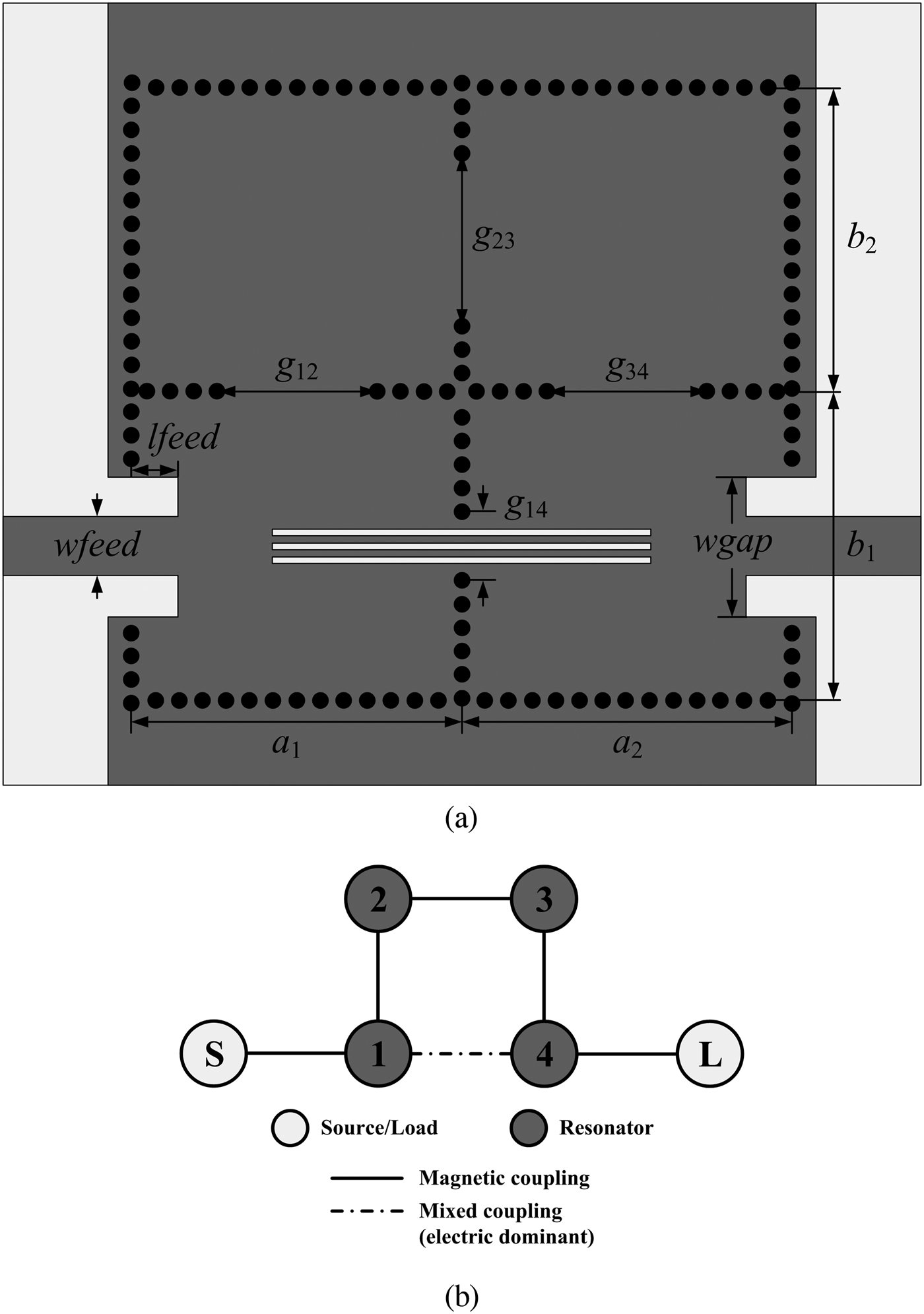
Fig. 11. Fourth-order cross-coupled bandpass filter: (a) configuration; (b) coupling topology.
The design parameters for the filter with the center frequency of f 0 = 10 GHz and absolute bandwidth of BW = 1 GHz have been obtained using the relations given in (10) and are as follows:
 $$\eqalign{Q_e &= 9.63,\,\,\,\,\cr k &= \left[ {\matrix{ {} & {\bf 1} & {\bf 2} & {\bf 3} & {\bf 4} \cr {\bf 1} & 0 & {0.0845} & 0 & { - 0.0253} \cr {\bf 2} & {0.0845} & 0 & {0.0799} & 0 \cr {\bf 3} & 0 & {0.0799} & 0 & {0.0845} \cr {\bf 4} & { - 0.0253} & 0 & {0.0845} & 0 \cr}} \right].}$$
The dimensions of the optimized filter are as follows: a 1 = a 2 = 14 mm, b 1 = 13.15 mm, b 2 = 12.91 mm, g 12 = g 34 = 6.78 mm, g 23 = 7.34 mm, g 14 = 2.92 mm, l = 16 mm, w = 0.23 mm, s = 0.35 mm, lfeed = 2.03 mm, wfeed = 2.43 mm, and wgap = 6 mm. The synthesized response of the fourth-order cross-coupled bandpass filter corresponding to the coupling matrix (12) is shown in Fig. 12(a). The comparison between the simulated and measured results of the filter is presented in Fig. 12(b). A good agreement is observed between the synthesized and simulated responses. The photograph of the fabricated fourth-order cross-coupled bandpass filter is shown in the inset of Fig. 12(b). The measured results show that the center frequency of the filter is located at 10.13 GHz and the 1 dB FBW is 10.8%. The measured in-band insertion loss is below 1.5 dB and the measured passband return loss is better than 17 dB. The TZ below the passband is located at 9.35 GHz and the TZs above the passband are located at 11.04 and 12.73 GHz. The measured results are in good agreement with the simulated results. A frequency shift of 1.3% (130 MHz) in the center frequency of the filter was observed. The discrepancies in the measured results can be attributed to fabrication inaccuracy.

Fig. 12. Frequency response of the fourth-order cross-coupled bandpass filter: (a) synthesized; (b) simulated and measured.
Conclusion
In this article, a planar SIW structure with mixed electric and magnetic coupling implemented on a single-layer substrate has been presented. Three slot-lines are combined with a conventional iris-window between two SIW cavity resonators to build mixed coupling. The electric and magnetic coupling strengths can be independently controlled by adjusting the dimensions of the slot-lines and the width of the iris-window, and a controllable TZ located at the lower or upper stopband can be created. Third- and fourth-order cross-coupled filters using the proposed mixed coupling structure have been developed at the X-band to demonstrate the validity of the coupling structure. It has been observed that the simulated and measured results are in good agreement. The filters exhibit planar structure, low cost, good selectivity, easy fabrication, and easy integration with other planar circuits, which make it a suitable candidate for microwave applications.
 Amit Ranjan Azad received the B.Tech. degree in Electronics and Communication Engineering from West Bengal University of Technology, West Bengal, India, in 2010, the M.Tech. degree in Electronics and Electrical Communication Engineering from the Indian Institute of Technology Kharagpur, West Bengal, India, in 2012, and is currently working toward the Ph.D. degree at the Indian Institute of Technology Kharagpur. His current research interests include the synthesis, analysis, and design of microwave filters for wireless applications.
 Dharmendra Kumar Jhariya received the B.E. degree in Electronics and Communication Engineering from the Government Engineering College Rewa, Madhya Pradesh, India, in 2009, the M.Tech. degree in Electronics and Communication Engineering from Motilal Nehru National Institute of Technology Allahabad, Uttar Pradesh, India, in 2011, and the Ph.D. degree in Aerospace Engineering from the Indian Institute of Technology Kharagpur, West Bengal, India, in 2017. His current research interests include the analysis and design of ultra-wideband filters, bandstop filters, and dual-band filters. Since 2017, he has been a faculty member with the Department of Electronics and Communication Engineering at Jaypee Institute of Information Technology, Noida, India.
 Akhilesh Mohan received the B. Tech. degree in Electronics Engineering from Kamla Nehru Institute of Technology, Sultanpur, India, in 2002, and the M.Tech. and Ph.D. degrees in Microwave Engineering from the Indian Institute of Technology Kanpur, Uttar Pradesh, India, in 2004 and 2009, respectively. From 2009 to 2010, he worked as a Scientist at the Space Applications Center, Indian Space Research Organization, Ahmedabad, India. From 2010 to 2013, he was a faculty member with the Department of Electrical Engineering at the Indian Institute of Technology Jodhpur, Rajasthan, India, where he was involved in teaching and research activities. Since 2013, he has been a faculty member with the Department of Electronics and Electrical Communication Engineering at the Indian Institute of Technology Kharagpur, West Bengal, India. Dr. Mohan has authored or co-authored more than 80 peer-reviewed international journals and conference papers. He is a member of IEEE. His research interests include the design of microwave filters and planar antennas for wireless communication systems.


