I. INTRODUCTION
Patten reconfigurable antennas allow wireless systems to be self-adapting in various propagation circumstances, with better reception, higher propagation efficiency, and less interference. Phased arrays and reflect-array systems offer the best radiation pattern diversity. However, they are bulky and use costly components. Alternatively, cost effective reconfigurability can be obtained by introducing switch circuitry into the simple antenna structures.
Previous studies proved that the single-arm rectangular spiral antennas (SARSAs) can be designed to steer the beam into different azimuth directions. The basic SARSA presented in [Reference Nakano, Eto, Okabe and Yamauchi1] offers a tilted beam fixed around 30°from the central axis. In [Reference Mehta, Mirshekar-Syahkal and Nakano2], the pattern reconfigurability is obtained by short-circuiting the spiral arm to the ground at certain points. In [Reference Huff and Bernhard3], packaged radio frequency micro-electromechanical system (RF-MEMS) switches are integrated into a resonant square-spiral microstrip antenna, to reconfigure its radiation pattern between the endfire and broadside. In [Reference Pan, Bernhard and Nair4], the switches are attached in the gap of the spiral, making both the radiation pattern and frequency reconfigurable. Better reconfigurability is achieved by integrating RF-MEMS switches along the spiral arm to manage its length [Reference Chang won, Ming-jer, Li and De Flaviis5]. Still, none of these antennas can cover azimuth space wider than 90°. In [Reference Deo, Mehta, Mirshekar-Syahkal and Nakano6], nearly a full-range cover of the azimuth plane is realized with the help of high-impedance surface (HIS). Although thickness of the antenna substrate is greatly reduced by utilizing the HIS, its area size increases considerably. Moreover, no actual switches are attached, and no practical biasing method is provided.
In [Reference Liang, King Yuk and Ramer7], we proposed a novel SARSA, capable of covering wider azimuth space. Its novelty lies in having additional bridges attached between different turns of the spiral and the critical switches added in the center. Unlike [Reference Pan, Bernhard and Nair4], extra switches near the bridge serve to stop the flow of the current in the opposite direction along the spiral. In simulation, RF-MEMS capacitive switches have been used to achieve the best possible performance. While RF-MEMS switches have remarkable performance in terms of insertion loss, isolation and linearity, their fabrication process is costly and time consuming. Furthermore, the seven RF-MEMS switches need seven DC signals to bias successfully. Multiple bias lines have to be laid underneath the spiral arm; then cross talk and coupling may ensue.
This paper reports a cost effective solution using printed circuit board (PCB) panels and PIN diodes. Some of the switches are connected in series; this enables biasing with no more than three DC signals. In the last section we give a systematic comparison, over all the key features, of our design with those found in the open literature.
II. DESIGN CONSIDERATIONS
To confirm the possibility of achieving wider azimuth coverage with a structure similar to the existing designs, the dimensions that were used in [Reference Nakano, Eto, Okabe and Yamauchi1] and [Reference Mehta, Mirshekar-Syahkal and Nakano2] have also been used here. As a result, our device operates at 3.3 GHz. The antenna is designed using Rogers 4350 substrate with dielectric constant 3.66 and thickness 11.43 mm; approximately a quarter-wavelength at the operating frequency. The spiral arm, shown in Fig. 1, starts with a unit length segment a = 4.8 mm and increases progressively: a, 2a, 2a, 3a, 3a … 7a, 7a, 8a, with the arm width set to 1.4 mm. The central top metallization is connected to the SMA connector with a pin through the substrate.

Fig. 1. The geometry of the beam-steering spiral antenna: (a) top view and (b) perspective view.
The reconfigurability is achieved by adding seven switches and two bridges to the antenna; a gap of 1 mm is reserved for each switch. Their positions are critical to generating the desired beam directions. Chang won et al. [Reference Chang won, Ming-jer, Li and De Flaviis5] simplified the beam steering of a spiral antenna by considering only the length of spiral arm. However, to model more accurately, the segments that have been cut off by the switches have to be considered as well. It is because the couplings between different segments are strong and cannot be neglected.
All of the simulation work in this paper was performed using Ansys HFSS. As yet, no theoretical equations have been developed to predict the positions of the switches; the work relied, in the main, on simulation and parametric sweep. Switches and bridge locations can be determined with the aid of the surface-current density plots produced by simulators.
Firstly, a bridge (BR1) and three switches (SW1, SW2, and SW3) are placed at the innermost part of the spiral. As they are located near the feeding point and in the highest current density area, they play the most significant role in altering the current distribution and are re-forming the spiral.
Therefore, the design process begins with the structure with only three switches attached in the spiral center. In Fig. 2, picture (b) presents the complex magnitude for the distribution of the current density over the spiral, when both SW1 and SW3 are ON, and SW2 is OFF; picture (d) is for the opposite settings. The simulated 3-dimensional (3-D) radiation patterns (in top views (c) and (e)), show beam directions, respectively, in −Y and +X in azimuth plane. Figure 2(a) shows the scale shared by all the current density plots in Figs 2 and 3.

Fig. 2. Current density plots for spiral antenna with only three switches and one bridge defined. RHCP radiation patterns are shown to the right, with peak value in red and green indicating around 3-dB lower than the peak: (a) scale for current density plots; (b) SW1 is ON, SW2 is OFF, SW3 is ON; (c) radiation pattern for (b); (d) SW1 is OFF, SW2 is ON, SW3 is OFF; and (e) radiation pattern for (d).

Fig. 3. Current density plots for spiral structure with BR2 added: (a) SW1 is ON, SW2 is OFF, and SW3 is ON; (b) radiation pattern for (a); (c) SW1 is OFF, SW2 is ON, SW3 is OFF; and (d) radiation pattern for (c).
Another bridge (BR2) between the outer turns can transform, from a certain point, the single-arm spiral into a two-arm spiral. It is a metal strip connected to the spiral arm. While SW4 determines the current flow, SW5 is used to stop the current flowing in the opposite way; otherwise cross polarization would increase. Once the position for BR2 is defined, the positions for SW4 and SW5 are determined. Normally, BR2, SW4, and SW5 can be placed into current dense zones, like 1○ and 2○ marked in Figs 2(a) and 2(c), to steer the beam significantly. Reference [Reference Liang, King Yuk and Ramer7] chose 1○ for the position of the BR2 and achieved two back-to-back directions. In this article we select 2○ to seek for more of the available directions.
Figure 3 illustrates the current density distribution and the radiation patterns for two cases with current flowing thorough BR2. They are beaming in the −X and +Y directions.
It is worth noting that [Reference Pan, Bernhard and Nair4] also has similar bridges placed in the gap of the spiral. However, there are no elements to help cut out the spiral arm near the bridges. In this work, SW3 and SW5 are used to stop the current from flowing clockwise, lest it generates unwanted left-hand circular polarization (LHCP) radiation after passing through the bridges.
Two more switches, SW6 and SW7, are added along the spiral arm to further increase the gain and optimize the cross-polarization. To avoid a considerable reshaping of the pattern, the areas of less dense current are selected for locating the switches.
All these cases have to be inspected simultaneously, thus the trade-off between the gain, return loss, and polarization purity has to be carried out in the design phase. Parametric sweep is necessary for satisfying the expected specifications. Positions of BR2, SW6, and SW7 should slide along the spiral arm (e.g. for BR2, all positions along the second spiral turn in 1 mm increments) to optimize the desired beam direction for each case. For applications run at different frequency, spiral arm width, unit length a, and substrate thickness (as in Fig. 1(a)) also need to be adjusted; they are inverse proportional to the operating frequency.
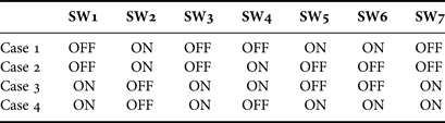
Figure 1 shows the spiral structure with all switches. Table 1 lists the combinations of the states of switches that produce the separated beam directions. They are labeled as Cases 1–4.
Table 1. State of the switches.

The MA4AGBLP912 PIN diode model from M/A-COM used in the design gives the series resistance of 4 Ω in the ON-state, total capacitance 28 fF, and isolation 30 dB in the OFF-state. Current threshold for switching the diode is around 10 mA. Typical voltage at which 10 mA current is obtained is approximately 1.4 V.
The orientation settings of the diodes are also shown in Fig. 1(a). DC biasing voltages are required to be connected with spiral arm to input bias signals. Three DC bias signals, DC1, DC2, and DC3, along with a DC ground, are connected to the spiral arm to actuate the switches. DC1 can be superimposed through the inner conductor of the coaxial cable by a bias-tee, while DC2 and DC3 are biased using side biasing pads.
Figure 4 provides an equivalent circuit for the biasing purposes. Both positive and negative voltages are required to satisfy the switch states for Case 1–4. For example, voltages of −2.8, −1.4 and 0 V are to be set for DC1, DC2, and DC3, respectively, to enable Case 2. For the measurements, we use resistors of 68 Ω to limit the current increment and to prevent damage. Extra Ampèremeters are used for monitoring the current. The resistors and ampere meters are not mandatory when the voltage can be adjusted very precisely.

Fig. 4. Bias-equivalent circuit.
III. FABRICATED ANTENNA
As a panel of thickness of 11.43 mm is not available for Rogers 4350, multiple thinner laminates are stacked together to construct the substrate. Here seven laminates of 1.524 mm and one of 0.762 mm are stacked together to accumulate the needed 11.43 mm. The air gaps between laminates introduce loss and interference; this can be minimized by tightening the four plastic screws located in the corners. In commercial manufacture, these laminates can be glued together using multilayer technology. The same model of diode is used for the fabricated antenna: two pads of width 0.2 mm are added to attach each PIN diode.
DC2 is connected to the spiral arm segment that is connected to the cathode of SW4. As a result, a bypass is needed to avoid the outermost turn of the spiral. Therefore, two via holes are drilled and a copper trace is also placed on the backside of the first laminate as shown in Fig. 5(b).

Fig. 5. Geometry of the antenna: (a) Top view and (b) Perspective review.
In general, bias networks and filters, which consist of capacitors and inductors, are necessary for biasing PIN diodes to prevent RF energy from flowing through the DC channels. Drilling via holes is unavoidable as a result. However, in this design, the substrate is too thick, making difficult the via holes from the top to the bottom ground layer. Instead, quarter wavelength stubs that make the RF signals open-circuit are applied.
Both biasing lines and matching stubs are a quarter-wavelength to ensure that the signals are open-circuited at the pads. The positions of the quarter-wavelength stubs together with the biasing pads also can be selected based on the current density distribution plots. Lower current-density areas are recommended for their locations, in order to minimize interference. Since various cases have different current distribution, parametric sweep is needed to find the best positions for these stubs to optimize performance.
Figure 5 shows the spiral antenna geometry with biasing lines, pads, and quarter wavelength stubs. Figure 6 provides a glimpse of the fabricated antenna.
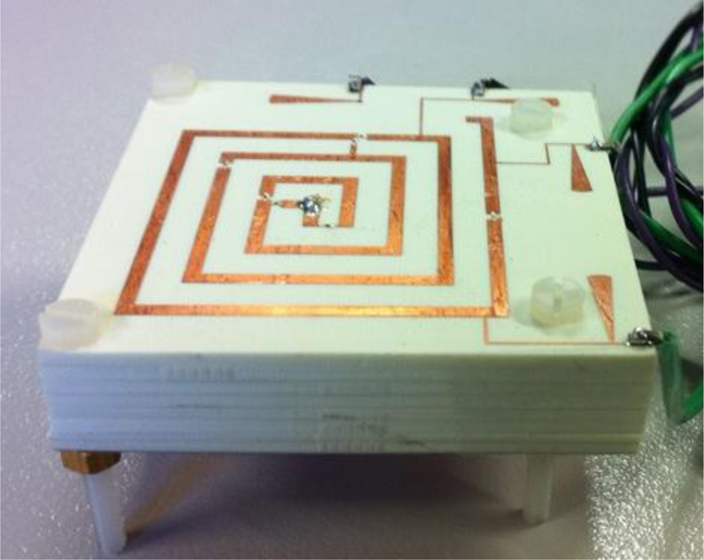
Fig. 6. Photograph of the fabricated antenna ready for testing.
IV. MEASUREMENT RESULTS
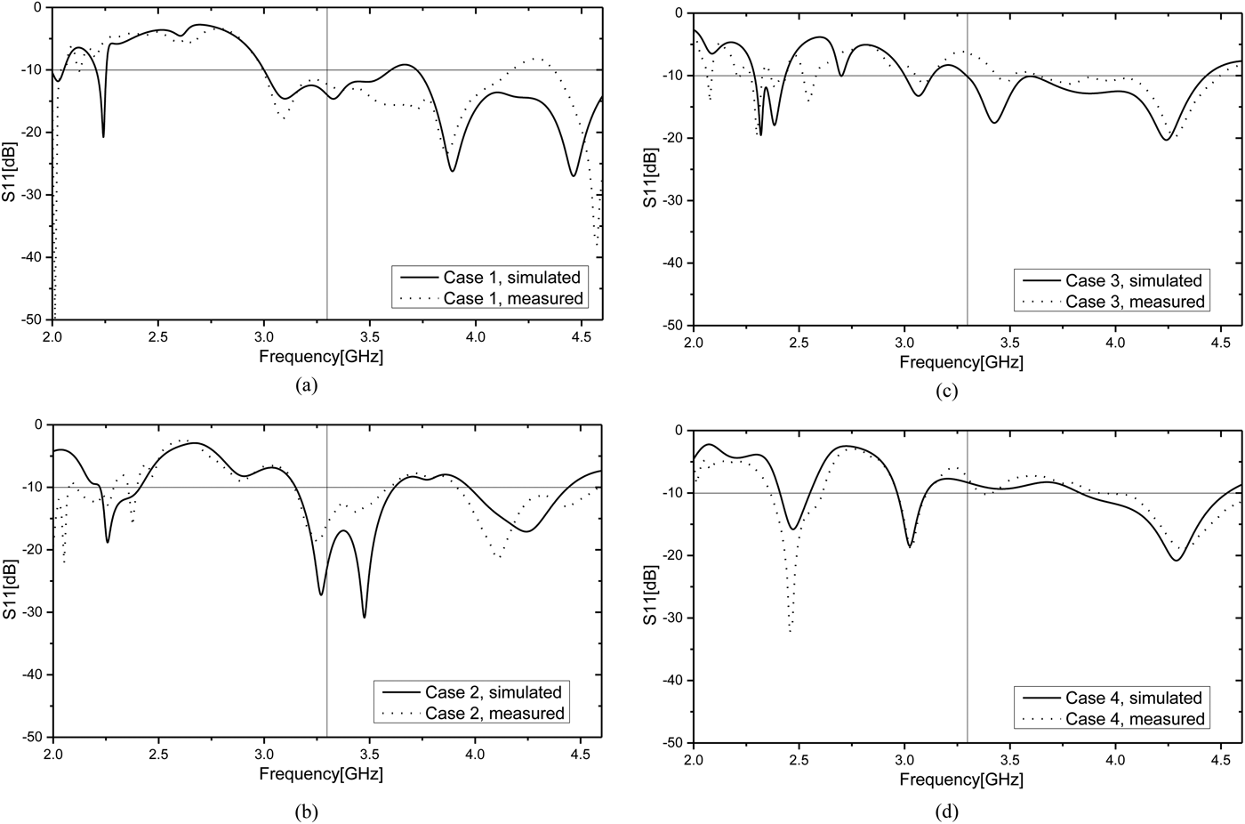
All of the measurements were carried out in an anechoic chamber at the CSIRO. The gain and radiation pattern measurement method is described in more detail in [Reference Bee Yen, Cahill and Fusco8]. S-parameter is measured using Agilent E8363B PNA Network Analyzer. Figure 7(a–d) shows both the simulated and measured S-parameters for various cases. It can be seen that the return loss is better than 10 dB for Cases 1 and 2, and better than 8 dB for Cases 3 and 4. The mismatch occurs mainly because of the coupling effects due to the biasing line beneath the spiral arm. In practice, an extra matching network can be introduced to further improve matching.

Fig. 7. Simulated and measured S11 for all four cases: (a–d) – Cases 1–4.
For radiation pattern measurement, theoretically, it would require 3-D radiation pattern and gain measurements to determine the maximum beam directions and gain for such tilted beam antennas. However, that requires too many measurements for various cases at various frequency points. Therefore, the actual measurements are based on the simulated max phi and then the radiation patterns are plotted with respect to theta.
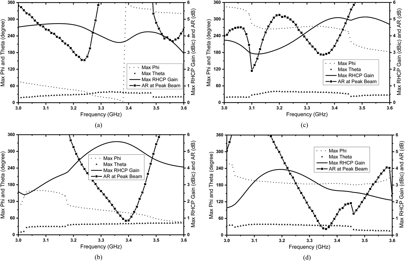
The maximum beam directions and the peak gains depend on frequency. Figure 8 provides a view for such dependence by showing the simulated maximum right-hand circular polarization (RHCP) gain, the direction (phi, theta) in which this gain is achieved, and the axial ratio (AR) at peak beam directions.

Fig. 8. Frequency dependence. (a) Case 1; (b) Case 2; (c) Case 3; and (d) Case 4.
Data are generated only in frequency range 3.0–3.6 GHz for this antenna. The gain drops dramatically outside this frequency range and the main beam may split. Even in this frequency range, the gain, as well as max phi, fluctuates considerably. Nonetheless, they are relatively stable for all the cases over 200 MHz, with the band centered at 3.3 GHz. Therefore, the radiation pattern measurements are only conducted at 3.2, 3.3 and 3.4 GHz, respectively.
Figure 9 shows the radiation pattern measurement configuration. One should note that the azimuth direction is only adjusted manually by rotating it on the antenna stand. A digital protractor is used to set it at the 90° angle.

Fig. 9. Measurement configuration – the azimuth angle (phi) is manually adjusted.
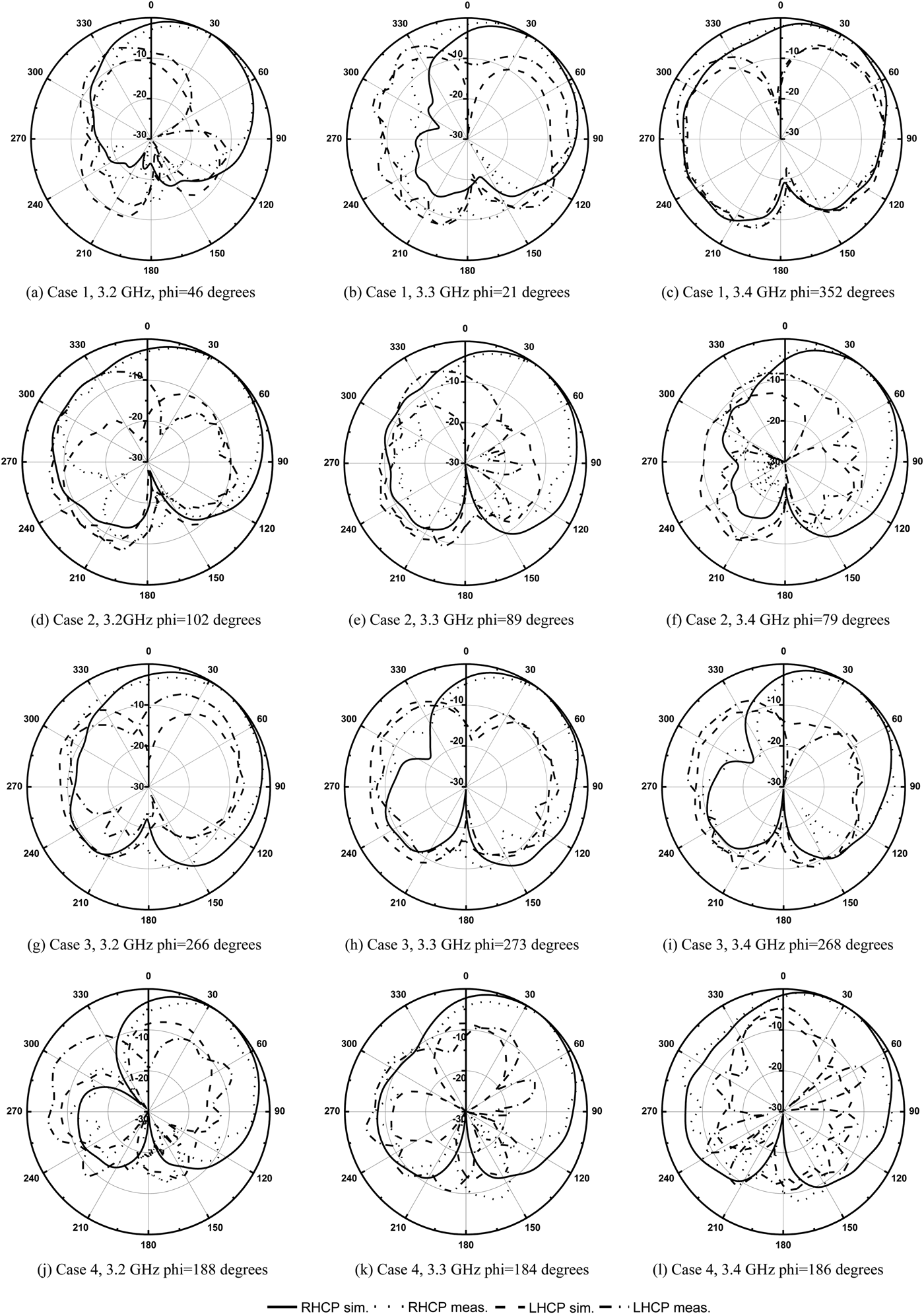
Both the simulated and measured radiation patterns for both LHCP and RHCP are shown in Fig. 10. The measured RHCP patterns seem to follow the same trend as the simulated ones. The measured LHCP results do not always resemble the simulated ones; this suggests possible polarization degradation. This could be due to biasing cables attached to the biasing pads, the uncertainty in the location of small structures like the blind holes and the thin line beneath the spiral. The former cannot be fully accommodated in the simulation frame, even though several quarter-wavelength stubs have been applied to open circuit the RF signals for the cables. The latter may introduce a significant error in the simulation process because of the mesh level and precision of the PCB fabrication.

Fig. 10. Radiation patterns at 3.2, 3.3, and 3.4 GHz for Cases 1–4.
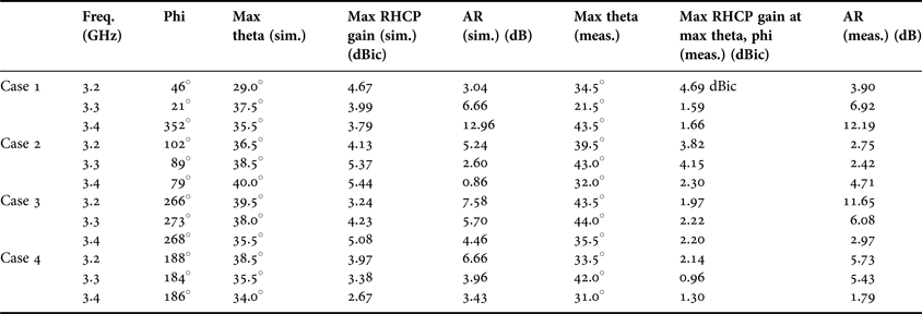
Table 2 summarizes relevant parameters for all the cases in our design (at different frequency points: 3.2, 3.3, 3.4 GHz), in terms of their maximum beam directions, maximum gain, and the AR in this direction. Since there was no sweep for the azimuth plane angle, neither the maximum gain nor the related beam directions can be found. Therefore, the gains in Table 2 are the gains in the directions defined by phi and theta, rather than max gain.
Table 2. Summary of the simulated and measured maximum beam directions and RHCP gains (simulated); AR-at-peak and RHCP gain directions (measured).

Measured data do not coincide with the predicted ones, suggesting the beams may have shifted away from the simulated max beam directions. This is mainly due to the buried thin conducting line and two blind holes necessary for biasing. Their coupling with the spiral arm has caused significant interference, which reduces the gain and impairs matching. The line has to be as thin as possible to minimize this coupling effect. On the other hand, simulation and fabrication errors increase as the structure becomes smaller, which makes the prediction of radiation pattern less accurate.
The discrepancy may also lie in the conductor loss and poor manual alignment of the azimuth angle with the simulated max phi. In addition, the biasing lines, pads and open-circuit stubs, even though finely tuned, become radiating elements of the antenna, making inevitable some performance deterioration. Errors can also be caused by the bias voltage source, multimeters, or cables placed in the anechoic chamber, as well as from the interference caused by the wire connected to the biasing pads.
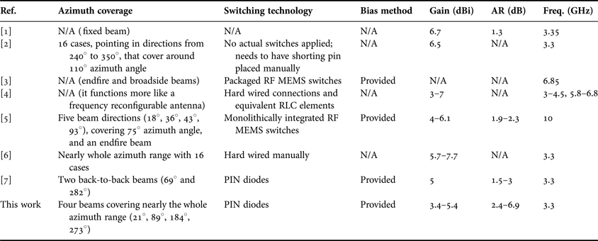
V. COMPARISON WITH EARLIER DESIGNS
We compare our design in Table 3 with those earlier proposed in the literature, indicating the reference numbers of the relevant papers. We address six key features: azimuth coverage, switching technology, bias method, gain, AR at the peak beam, and the operating frequency. We use N/A for ‘not available’ – when it was not discussed in the surveyed paper. As shown in the table, our design makes certain compromises in gain, polarization, and matching, to achieve larger azimuth coverage with automatic switching.
Table 3. Summary of design features.

VI. CONCLUSIONS
A beam steering spiral antenna is realized using PIN diodes as switches. Wide beam coverage is achieved around 3.3 GHz. Antenna radiation patterns are plotted at 3.2, 3.3, and 3.4 GHz. RHCP patterns are almost identical to the simulated patterns, while a large discrepancy occurs for LHCP ones. Measured RHCP gains are much lower than the predicted maximum beam directions due to poor alignment, to the attached cables required by DC biasing currents, and, especially, to the coupling of the thin line under the spiral arm. Although there is some disagreement between the simulations and measurements, the present work validates the proposed solution for a reconfigurable spiral antenna and gives confidence to its possible RF-MEMS version.
ACKNOWLEDGEMENTS
The authors are grateful to June Chan and Jacky Hou from Rogers Co. for providing guidance on substrate panel selection; to Carl Tengstrom from Lintek for assistance in the PCB fabrication; to M. Shen for implementing the attachment of the PIN diodes. Especially acknowledged is Dr. Ken Smart, CSIRO ICT, for his assistance with antenna measurements.
 Liang Gong received his B.Eng. degree in Electrical Engineering from the Xidian University, Xi'an, China in 2008. From 2008 to 2011, he worked as an electronics engineer in a research institute in China. Since 2012, he has been studying in the School of Electrical Engineering and Telecommunications, University of New South Wales. He finished his Masters by Research program in mid-2013 in the field of reconfigurable antennas and is currently a Ph.D. candidate. His research interests include the RF MEMS enabled microwave devices, millimeter-wave circuits and systems, filters and antennas.
 Rodica Ramer received a B.Sc. degree in engineering physics, ME in electrical engineering and Ph.D. in the solid state physics in 1989, all from the University of Bucharest. Dr Ramer joined the University of New South Wales (UNSW), in 1993, where she is a professor in the School of Electrical Engineering and Telecommunications, leading the microwave, millimeter-wave and electromagnetics group. She has held guest and visiting professorship positions at many Universities around the world. Her research activities have been in the area of microwave devices and materials and EM techniques. She has authored and co-authored over 250 refereed papers and a number of book/chapters and patents. Her current research involves advancements in RF MEMS and SIW technologies. Dr. Ramer is a senior member of IEEE MTT-S, AP-S and Com.Soc., and a fellow of Electromagnetics Academy. She has held key positions and has served on various panels and international committees and international conferences/symposia. She has served on editorial/review boards of several journals and conferences.
 King Yuk (Eric), Chan received his B.Sc. (with first class honors) and M.EngSc. degrees in Electrical Engineering from the University of New South Wales (UNSW), Sydney, Australia in 2005 and 2006. He then continued his Ph.D. degree in electrical engineering under a joint project between the University of New South Wales (UNSW) and the Center for Integrated RF Engineering (CIRFE), University of Waterloo, Canada. From 2007 to 2008, he was a research assistant at CIRFE, University of Waterloo. He received a Postdoctoral Fellowship from UNSW in 2010. He was a Postdoctoral Fellow at CSIRO ICT Centre, Sydney, NSW, Australia from 2011 to 2013 and he is currently a Research Associate at UNSW. His expertise includes passive and active circuits from 500 MHz to 110 GHz, reconfigurable RF-frontend including frequency and radiation reconfigurable antennas, tunable filters, impedance matching networks, phase shifters, and switching networks.