I. INTRODUCTION
Modern high-speed electronic circuits often employ mixed signal systems, where digital and analog/RF circuits are placed on the common power and/or ground planes. Maintaining the signal and power integrity under such circumstances are highly desirable throughout the process of designing the chip, package and circuit boards. The high-speed circuits give rise to simultaneous switching noise (SSN) [Reference Senthinathan and Price1] also referred as ground bounce noise (GBN) while switching between high- and low-voltage levels simultaneously. This SSN can propagate between power/ground plane pairs and may affect the signal and power integrity of the whole system. In the past, several techniques have been employed to tackle the problem of SSN. Use of decoupling capacitors at chip, package, or circuit level is one of the most common methods employed to suppress the SSN. However, the band-limited characteristics of the decoupling capacitors restrict their use only below the self-resonance frequency. Use of the electromagnetic band gap (EBG) [Reference Abhari and Eleftheriades2] structures on the other hand is a very promising technique employed in suppressing SSN. The periodic patterns of EBG structures etched over power or ground plane offer high impedance and help to attenuate the propagating SSN. In the past several configurations of EBG structures have been employed for this purpose. In [Reference Wu, Wang, Lin, Wang and Chang3], an L-shaped band-gap structure was proposed which had a band gap of 4 GHz along with the SI analysis. In [Reference Zhou, Zhao and Feng4] a fractal EBG structure offering a stop band of 4 GHz was proposed without presenting any analysis of signal integrity. A wide band-gap structure with a band gap of 15 GHz was proposed in [Reference Kwon, Sim, Kwak and GwanYook5] excluding the signal integrity analysis. In [Reference Wu, Lin, Wang, Wang and Chen6] a band-gap structure with a band gap of 4 GHz was designed and also the signal integrity analysis of the structure was presented. Another structure has been proposed to mitigate GBN in [Reference Xu, Zhao and Feng7] offering a band gap of only 5 GHz. Also signal integrity analysis was presented for this structure. In [Reference Rao and Swaminathan8, Reference Rao9] a band-gap structure of 3.5 GHz was proposed along with the analysis of signal integrity. In [Reference Rao10] a wide band EBG with a band gap of 40 GHz was presented, however, analysis of signal integrity was not dealt with. In [Reference Shi, Cai, Meng and Cheng11] a simple EBG with a band gap of 20 GHz was proposed. Also the signal integrity analysis was presented. The proposed structure offered a band gap of 20 GHz and the signal integrity analysis depicted degradation in maximum eye open (MEO) and maximum eye width (MEW) as 8.57 and 7.69%, respectively.
The band-gap characteristics can be obtained from reflection phase, dispersion diagram, or transmission characteristics. However, the transmission response itself is sufficient for predicting the band-gap characteristics [Reference Wu, Lin, Wang, Wang and Chen6–Reference Rao9]. The dispersion diagram on the other hand gives the exact details of band-gap characteristics, but it requires much higher computational time and the time complexity increases with the complexity of the structure.
In the present paper, a simple EBG structure is proposed that provides a wide band gap of 20 GHz. The proposed structure consists of three square patches inter connected by L-shaped bridges. Two of three patches were shorted to the ground plane using vias. The unit-cell dimensions were taken to be less than half the operating wavelength at 2 and 2.5 GHz, at which the structure has been analyzed for signal integrity. Generally to provide good solation (band gap) characteristics 4–5 unit cells are needed [Reference Hung, Lin, Wu and Wu12], which increases the physical space required for incorporating the EBG. Therefore, the proposed EBG is designed to provide good suppression characteristics even with a single cell. The proposed structure offers an isolation of −30 and −40 dB for 20 and 15 GHz bandwidths, respectively, for a single unit cell. The transmission characteristics of the single-cell EBG are calculated from the experimental results of the fabricated structure. The signal integrity analysis is also carried out. Both simulation and experimental results are presented.
II. PROBLEM FORMULATION
The motivation behind the proposed work is to design a simple planar EBG structure to provide wide band gap and good signal integrity. The conventional linear bridges consisting of straight micro-strip lines in the planar EBG have been modified. In the proposed design, instead of straight micro-strip connecting bridges, L-shaped bridges with a center patch are used resulting in a structure whose unit cell is shown in Fig. 1. The front view of the EBG is shown in Fig. 1(b). The dimensions of the EBG are also shown. This is designed using IE3D simulation software and fabricated on a FR4 Epoxy substrate with relative permeability of 4.4 having 5.5 cm × 4 cm dimensions.

Fig. 1. (a) Top view and (b) front view of unit cell of a proposed planar EBG structure.
All the square patches in the unit cell have the same dimensions.
The design parameters are as follows:
c = 12.76 mm, g = 1.2 mm, L = 5.5 cm, and W = 4 cm.
The design is implemented on an Epoxy FR4 substrate with thickness 1.58 mm, and a prototype model is developed. The fabricated model of the proposed structure is shown in Fig. 2. The ports are placed at the locations just ahead of the via shorts (approx. 1.5 mm).
Fig. 2. Proposed planar EBG structure: (a) top view and (b) bottom view.
III. EXPERIMENTAL RESULTS
The fabricated model is tested using vector network analyzer (VNA) and S-parameters are obtained and compared with the simulation results. The S-parameters are shown in Fig. 3(a). The measurement results obtained using VNA are shown in Fig. 3(b). From Fig. 3(b) it can be seen that the transmission characteristics are below 30 dB from 10 MHz to 20 GHz. The stop band characteristics of the EBG are given in Table 1.
Fig. 3. (a) S-parameters of the proposed planar EBG structure. (b) S-parameters of the proposed planar EBG structure obtained using VNA.
Table 1. Stop-band characteristics of the proposed EBG
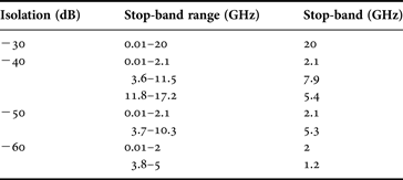
The proposed structure provides an isolation of −30, −40, −50, and −60 dB over a stop band of 20, 15.4, 7.4, and 3.2 GHz, respectively.
IV. SIGNAL INTEGRITY (SI) ANALYSIS
The SI analysis determines the highest data rate with which a digital signal can be sent through the signal trace. Even though the proposed EBG structure shows a wide band noise suppression its effect on the signal propagation should also analyzed. In this section, the SI for the proposed EBG structures is investigated in time domain using the eye diagram. The SI analysis is performed by generating an eye diagram, which determines the quality of the signal. From the eye diagram, (MEO in mV) for noise margin and (MEW in ps) for jitter margin are analyzed.
For the SI analysis a three-layer printed circuit board (PCB) stack-up as shown in Fig. 4 is considered and two different cases considering with and without the EBG unit-cell configurations are compared. The stacked configuration consists of a ground plane, a power plane, and a signal layer. A signal trace passes on top of the power plane, which is placed at a height of 1.58 mm from power plane. Two reference boards, one without an EBG configuration and second reference board with power plane employing the EBG unit cell are analyzed for SI.
Fig. 4. Isometric view of three-layer PCB with EBG power plane.
The signal propagates on the top signal layer through a signal trace. This layer has a thickness (h) of 1.58 mm having relative permeability of 4.4 and is placed on top of the EBG layer. The signal trace is designed as a 50 Ω line.
The eye patterns are generated for analyzing the signal quality by simulating the two-port S-parameters for the single-ended traces using method of moments (MoM)-based 2.5D solver IE3D. The advanced design suite tool is used to extract the wide band model from the S-parameters. The presence of the EBG power plane disturbs the signal integrity in high-speed digital circuits. A pattern of 27–1 pseudo-random binary sequence (PRBS), non-return to zero coded at 2 GHz is launched at the input of port 1 to obtain the eye diagram. Signal is fed at the input (Port 1), and the eye pattern is monitored at the output (Port 2). The inserted PRBS is coded with a data rate having 1 V swing and normalized rise/fall time is 200 ps. Figures 5(a) and 5(b) show the eye patterns with and without the EBG configuration in the power plane.
Fig. 5. Eye pattern: (a) without EBG power plane and (b) with EBG power plane at 2 Gbps.
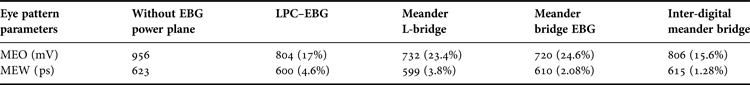
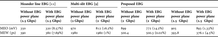
The quality of eye patterns is determined by the MEO and MEW values. It is seen that, for the PCB without the EBG power plane MEO = 899 mV and MEW = 0.5004 ns. For the case, when the EBG configuration is placed in the power plane, MEO = 772 mV and MEW = 0.5003 ns. Compared with the PCB without EBG power plane, the degradation of the MEO and MEW of the PCB with single-cell EBG power plane is about 14.2 and 0.02%, respectively. These values are comparable with the multi-slit EBG [Reference Xu, Zhao and Feng7], where the MEO degradation is 16.2% and MEW degradation is 1% for a similar data conditions. This mild degradation is acceptable in high-speed circuits. A comparison of the eye pattern parameters obtained from the various results available in the literature is shown in Table 2. Furthermore, a comparison of these parameters is also shown for the proposed structure in Table 3.
Table 2. Comparison of various planar EBG configurations [Reference Shi, Cai, Meng and Cheng11]
Table 3. Comparison of the proposed EBG with multi-slit EBG
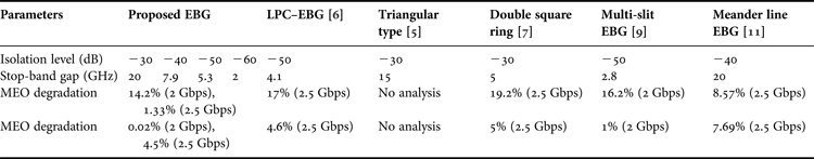
An overall comparison of all relevant parameters is shown in Table 4. The table gives a comparison of stop band gap along with the SI analysis.
Table 4. Comparison of the proposed EBG with other structures
V. CONCLUSION
A novel band-gap structure that provides an isolation of −30 dB over a large frequency band from 0.01 to 20 GHz is designed. The single-cell structure shows an isolation of −40 and −50 dB over a stop band of 15.4 and 7.4 GHz, respectively. The prototype model of the unit cell is fabricated and tested using the VNA. The model is also investigated for the SI analysis using the eye diagram. The results obtained are compared with the results available in the literature. The proposed structure shows an improved performance in comparison with the other structures studied in the past both in terms of band-gap characteristics and SI. The authors intend to carry out the equivalent circuit analysis in their future research course.
Bhargav Appasani was born in India in 1990. He has completed his Bachelor in Engg. degree and Master in Engg. course in Wireless Communications from Birla Institute of Technology, Mesra, Ranchi, India in 2012 and 2014, respectively. He is currently working as an Assistant Professor in Electrical and Electronics Department of Ran Vijay Singh College of Engineering and Technology, Jamshedpur, India. His research interests include Optimization techniques, Genetic Algorithms, design and optimization of Electromagnetic Band gap structures.
Nisha Gupta was born in India in 1960. She received the Bachelor's and Master's degrees in Electronics and Telecommunication and Electrical and Electronics Engineering both from Birla Institute of Technology, Mesra, Ranchi, India and Ph. D. degree from the Indian Institute of Technology, Kharagpur, India. She was a postdoctoral fellow at the University of Manitoba, Canada from 1997 to 1998 before joining the Department of Electronics and Communication Engineering, Birla Institute of Technology in 1999 as a Reader. Currently, she is a Professor in the same department. She has authored and co-authored more than 100 technical journal articles and conference papers. Her research interests are Computational Electromagnetics, EMI/EMC, Antennas for Wireless Communication, and AI techniques in Wireless and Mobile Communication.