


Introduction
In recent years, great development of modern wireless communication systems leads to the ever-increasing demand for compact radio frequency (RF) devices. Some efforts [Reference Feng, Zhou and Che1–Reference Chen and Lin15] have been done to design the compact microwave components. Multimode resonators are adopted in [Reference Feng, Zhou and Che1, Reference Ma, Liang, Jayasuriya and Yeo2] to design the compact wideband bandpass filters (BPFs). To obtain more compact microwave components, quasi-spiral loaded multiple-mode resonator and folded multiple-mode resonator are employed in [Reference Mehdi and Mirzaee3, Reference Wang, Chu and Gong4]. An extremely miniaturized microstrip branch-line coupler is presented in [Reference Mehdi5] based on coupled lines.
Power dividers and BPFs are indispensable building blocks in many RF front-ends. Filtering power divider (FPD) presented in [Reference Song6–Reference Chen and Lin15] can realize power splitting and filtering functions simultaneously in the single component, which is an effective method to reduce circuit size of RF/microwave system. In [Reference Song6–Reference Jiang, Wang, Huang and Wang9], the bandpass filtering response is introduced in power divider by using dual-mode resonators. Coupled lines are adopted in [Reference Wu and Jiao10, Reference Zhang, Yu and Liu11] to design FPDs. Base on half mode substrate integrated waveguide, a novel FPD is proposed in [Reference Moznebi and Afrooz12]. FPDs with a wide upper stopband are presented in [Reference Zhao, Gao and Zhang13, Reference Zhan and Zhao14] by utilizing discriminating coupling. Net-type resonators are introduced in [Reference Chen and Lin15, Reference Chen, Huang, Shen and Wu16] to design more compact FPDs.
Based on coupling matrix filter theory, novel topology structures are proposed in this paper to obtain good passband selectivity and out-of-band rejection performances, and the detailed design procedures are also given. A novel three-line resonator loading with short-circuited transmission line stubs is adopted, which can enhance out-of-band rejection. The isolation performances can be improved by adding an isolating resistor (R) between the edges of shorted stubs. Moreover, this three-line resonator can be commonly adopted in other BPF and FPD structures.
Design concept
Layouts of the presented FPDs
Coupling scheme of a second-order Chebyshev bandpass power divider is exhibited in Fig. 1, where each circle represents a resonator and the solid line between resonators represents the coupling path. It can be observed from Fig. 1 that the coupling scheme of a second-order Chebyshev bandpass power divider is symmetric, which is helpful to realize high in-band isolation, low in-band magnitude, and phase imbalances. An isolating resistor (R) is placed between port 2 and port 3 to achieve good in-band isolation performance. According to reference [Reference Hong and Lancaster17], the coupling coefficients M 12, M 13 and external quality factors Q ei, Q eo should satisfy the equations (1 and 2) to achieve good second-order Chebyshev filtering response and equal power splitting performance.
 $$M_{12} = M_{13} = \displaystyle{1 \over {\sqrt 2}} \displaystyle{{FBW} \over {\sqrt {g_1g_2}}}, $$
 $$Q_{ei} = Q_{eo} = \displaystyle{{g_0g_1} \over {FBW}}.$$
Fig. 1. Coupling scheme of a second-order Chebyshev bandpass power divider.
Figure 2 shows the geometries of three designed FPDs. As exhibited in Fig. 2(a), the proposed FPD1 consists of three different short-circuited microstrip resonators. Resonator 1 displayed in Fig. 2(b) is a quarter-wave microstrip resonator with a via on its left and excited by the tapped transmission line. Moreover, resonator 2 depicted in Fig. 2(c) is a short-circuited quarter-wave microstrip resonator and excited by the tapped microstrip line. Resonator 3 has the same structure as resonator 2. According to the layout of FPD2 shown in Fig. 2(d), a half-wave transmission line is adopted in resonator 1′ to introduce one transmission zero (TZ; F TZ1) and obtain deeper out-of-band rejection level. Resonator 2′ (3′) given in Fig. 2(f) has the same structure as resonator 2 (3) in FPD1. Resonator 2″(3″) shown in Fig. 2(i) is a short-circuited quarter-wave coupled lines and excited by tapped microstrip line, and another TZ (F TZ2) is introduced in FPD3 to realize better out-of-band rejection level by adopting resonators 2″ (3″). Moreover, the short-circuited point and the tapped transmission line are located on different transmission lines of coupled lines.

Fig. 2. Geometries of proposed FPDs. (a) FPD1, (b) resonator 1 in FPD1, (c) resonator 2 (3) in FPD1, (d) FPD2, (e) resonator 1′ in FPD2, (f) resonator 2′ (3') in FPD2, (g) FPD3, (e) resonator 1′′ in FPD3, (f) resonator 2″ (3″) in FPD3.
Analysis of TZs
The input impedance of resonator 2″ (3″) shown in Fig. 2(i) can be calculated as equation (3), and the expression of transmission coefficients (S 21) can be deduced as equation (4). The TZ can be obtained when S 21 = 0, and S 21 = 0 will be satisfied when the value of Z in approaches zero or infinity. Thus, frequency (f TZ2) of TZ introduced by resonator 2″ (3″) can be expressed as equation (5). In FPD3, the electric length (θ) of coupled lines is about 3π/8. Based on equations (5), the TZ (f TZ2) operating at 2.67f 0 (6.53 GHz) will be produced by employing resonator 2″(3″). Figure 3 shows the frequencies of f TZ2 with various values of l 0 and g 3. According to Fig. 3, the frequency of f TZ2 will shift to lower band when the values of l 0 and g 3 increase. As observed in Fig. 3 that TZ (f TZ2) introduced in FPD3 approximately operates at 4.85 GHz when the values of l 0 and g 3 are selected as 16.0 and 2.8 mm, respectively.
 $$Z_{in} = -\displaystyle{\,j \over 2}((Z_e + Z_o)\cot \theta + (Z_e-Z_o)\csc \theta ),$$
 $$S_{21} = \sqrt {1-{\left( {\displaystyle{{Z_{in}-Z{}_0} \over {Z_{in} + Z{}_0}}} \right)}^2}, $$
 $$f_{TZ2} = \displaystyle{{n\pi} \over \theta} f_0{\kern 1pt} {\kern 1pt} {\kern 1pt} {\kern 1pt} {\kern 1pt} {\kern 1pt} {\kern 1pt} {\kern 1pt} {\kern 1pt} {\kern 1pt} (n = 1,2,3...).$$
Fig. 3. The frequency of f TZ2 versus (a) various l 9 with g 3 selected as 2.8 mm and (b) various g 3 with l 9 selected as 16.0 mm.
The simulated transmission coefficients (S 21) of three designed FPDs are plotted in Fig. 4 to illustrate the TZs in FPDs. Comparing the S 21 of FPD1 and FPD2, one TZ (f TZ1) centered at 3.11 GHz is introduced in FPD2 by employing a half-wave transmission line, and out-of-band rejection level below 6.74 GHz is greatly improved. As observed from Fig. 4, another TZ (f TZ2) locating at 4.85 GHz is produced in FPD3 by adopting short-circuited quarter-wave coupled lines. Compared with FPD1 and FPD2, the out-of-band rejection level in FPD3 is significantly enhanced.

Fig. 4. Transmission characteristics (S 21) of FPD1, FPD2, and FPD3.
Analysis of various resonators
To explain the operating mechanisms of various resonators, the simulated external quality factors of various structures are exhibited in Fig. 5. It can be observed from Figs 5(a) and 5(b) that external quality factors of resonator 1 and resonator 2 will become lower when the values of w m1 and l 0 increase. According to Fig. 5(c), the external quality factor of resonator 1′′ will become lower when the value of w m3 increases. According to Fig. 5(d), the external quality factor of resonator 2′′ (3′′) will become higher when the value of s c4 increases.

Fig. 5. External quality factors of various resonators, (a) resonator 1 in FPD1 with various values of w m1, (b) resonator 2 (2′) in FPD1 (FPD2) with various values of l 0, (c) resonator 1′′′ (1′) in FPD3 (FPD2) with various values of w m3, and (d) resonator 2″ in FPD3 with various values of s c4.
The simulated coupling coefficients of three designed FPDs with various distances between resonator 1 (1′,1′′) and resonator 2 (2′,2′′) are plotted in Fig. 6. As observed in Fig. 6, the coupling coefficients between resonator 1 (1′,1′′) and resonator 2 (2′,2′′) will become weaker when the distances (g 1, g 2, and g 3) get bigger.

Fig. 6. Coupling coefficients versus distances (g 1, g 2, and g 3) between resonators 1 (1′, 1′′) and 2 (2′, 2′′) in three presented FPDs.
Analysis of bandwidth and return loss
To further explain the operating mechanisms of proposed FPDs, the frequency responses of three FPDs with various values of distances (g 1, g 2, and g 3) are shown in Fig. 7. As observed from Fig. 7, the passband bandwidths of FPDs will be narrowed when the distances (g 1, g 2, and g 3) between resonator 1 (1′, 1″) and resonator 2 (2′, 2″) get bigger. Considering Fig. 6 and equation (1), the fractional bandwidth (FBW) of the presented FPDs will become narrow when the values of distances (g 1, g 2, and g 3) get bigger, which agrees with the conclusion drew from Fig. 7.

Fig. 7. Frequency responses of proposed FPDs with various distances between resonators 2 (2′, 2′′) and 3 (3′, 3′′). (a) FPD1 with various values of g 1. (b) FPD2 with various values of g 2. (c) FPD3 with various values of g 3.
Figure 8 depicts the frequency responses of the presented FPDs when resonators (1, 1′, and 1′′) are selected as various dimensions, and the specific dimensions of resonators (1, 1′, and 1′′) are exhibited in Table 1. It is seen from Fig. 8 that S 11 can be optimized by changing the dimensions of resonators (1, 1′, and 1′′).

Fig. 8. Frequency responses of proposed FPDs with various dimensions of resonators (1, 1′, and 1′′). (a) FPD1 with various dimensions of resonator 1. (b) FPD2 with various dimensions of resonator 1′. (c) FPD2 with various dimensions of resonator 1′′.
Table 1. Dimensions (unit: mm) of three proposed FPDs under different cases

Analysis of bridge
A bridge is added to introduce a half-wave transmission line in FPD2 (FPD3), and the bridge makes a great influence on the isolation performance. The isolation performances of FPD2 and FPD3 with and without the bridge are plotted in Fig. 9. As observed in Fig. 9 that isolation performances in FPD2 and FPD3 can be effectively improved by adding the bridge.

Fig. 9. (a) Isolation performances of FPD2 with and without the bridge. (b) Isolation performances of FPD3 with and without the bridge.
Design procedures of FPDs
The three presented FPDs with second-order Chebyshev bandpass responses were designed and fabricated with the following specifications. Take FPD3 as an example, the center frequency and FBW of FPD3 are f 0 = 0.9 GHz and FBW (0.1 dB ripple level) = 7.8%, respectively. The lumped circuit element values of the low-pass prototype filter with a 0.1 dB ripple level are found to be g 0 = 1, g 1 = 0.843, g 2 = 0.622, and g 3 = 1.3554. For the given FBW, the corresponding coupling coefficients (M 12, M 13) and external quality factors (Q ei, Q eo) can be calculated as 0.1025 and 8.028 based on equations (1–2).
As shown in Figs 5 and 6, the quality factors of resonator 1 (2, 1′′, 2′′) can be tuned by changing the values of w m1 (l 0, w m3, s c4), while the coupling coefficients between resonator 1 (1′,1′′) and resonator 2 (2′,2′′) can be adjusted by changing the values of g 1 (g 2, g 2). Accordingly, the detailed design procedures of FPD are summarized as following:
Step 1: Given center frequency (f 0), FBW, isolation, and out-of-band rejection performances of designed FPD.
Step 2: Calculate the values of M 12, M 13, Q ei, and Q eo based on equations (1–2).
Step 3: Design unit cells with specific Q ei, Q eo, and stopband performances, based on Fig. 2.
Step 4: Tune the distance between the deigned unit cells to achieve the required coupling coefficient, based on Fig. 6.
Step 5: Add an isolating resistor (R), and the isolation performance between port 2 and port 3 can be optimized by tuning the value of isolating resistor (R).
Step 6: Construct the initial layout, then simulation and optimization can be obtained by utilizing Advanced Design System software, based on Figs 7 and 8.
Step 7: Return to step (3) until the simulated results meet the requirements presented in step (1).
Experimental verification and discussion
For demonstration, three FPDs operating at 2.45 GHz are fabricated on the TLX-8 substrate with a relative dielectric constant of 2.55 and a thickness of 31 mil. The photographs and specific dimensions of designed FPDs are exhibited in Fig. 10 and Table 2, respectively. The sizes of FPD1, FPD2, and FPD 3 are 0.28 $\lambda _g$ *0.10λ g, 0.26
 $\lambda _g$ *0.12λ g, and 0.26
 $\lambda _g$ *0.14λ g (where λ g is the guided wavelength on the substrate at the center frequency).

Fig. 10. The photographs of fabricated FPDs. (a) FPD1, (b) FPD2, and (c) FPD3.
Table 2. Dimensions (unit: mm) of proposed FPDs

As shown in Fig. 11(a), the measured S 11 is >15 dB ranging from 2.37 to 2.56 GHz, and the minimum insertion loss in the passband is 3.96 dB. It can be seen from Fig. 11(a) that measured harmonic suppression in FPD1 extends to 2.68f 0 with the rejection level better than 24.0 dB. Simulated and measured isolation results of FPD1 are plotted in Fig. 11(b). As observed in Fig. 11(b), the measured S 22 of FPD1 is better than 10 dB during the operating band, and the measured isolation (S 23) is better than 13.3 dB from DC to 3.05f 0.
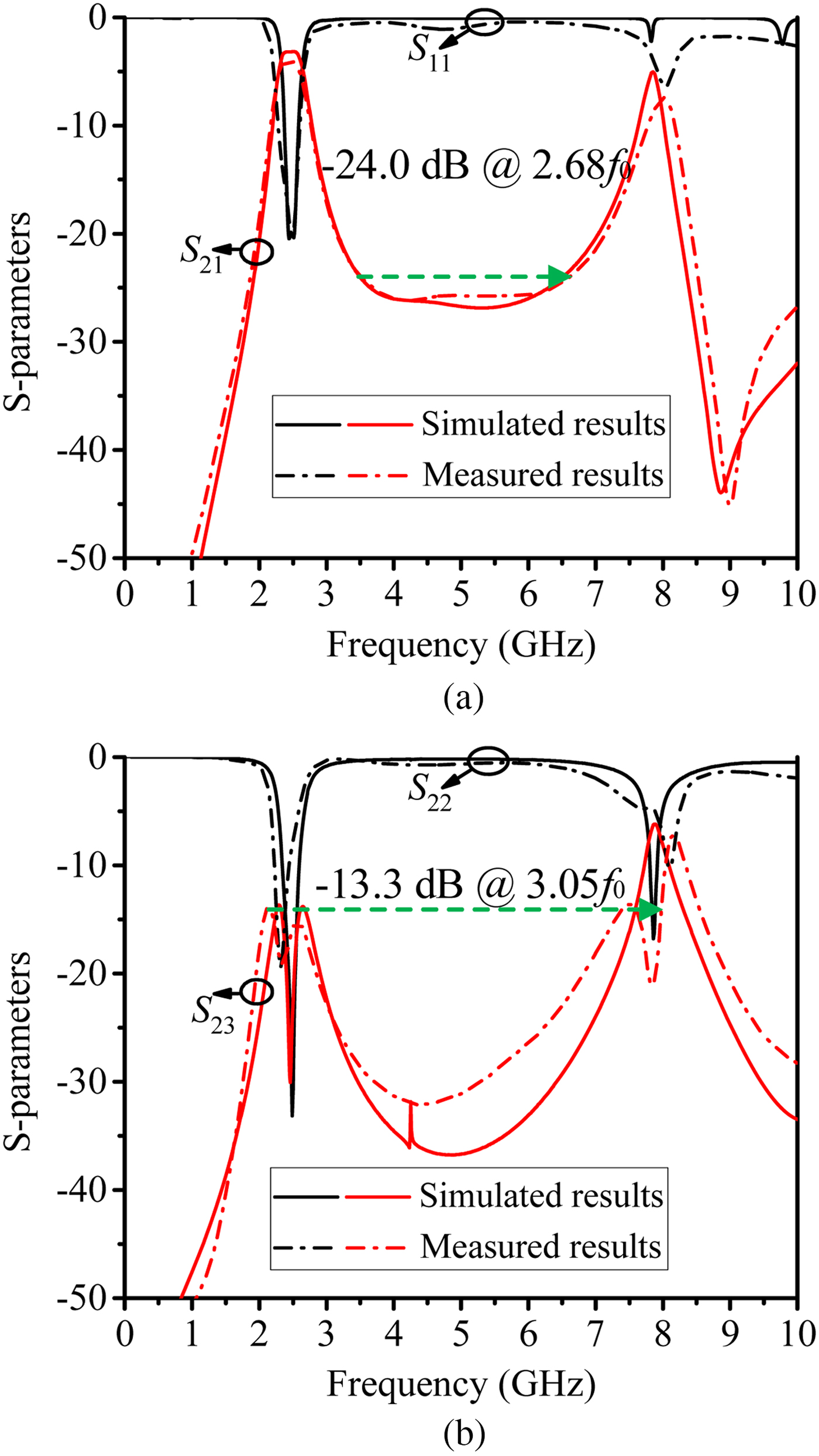
Fig. 11. Simulated and measured results of FPD1. (a) S 11 and S 21, and (b) S 22 and S 23.
According to simulated and measured results of FPD2 shown in Fig. 12(a), the measured S 11 is >10 dB ranging from 2.28 to 2.52 GHz, and the minimum insertion loss in the passband is 4.28 dB. It can be observed from Fig. 12(a) that the measured harmonic suppression in FPD2 extends to 2.75f 0 with the attenuation level better than 27.5 dB. Figure 12(b) depicts the simulated and measured isolation performances of FPD2. As shown in Fig. 12(b), the measured S 22 of FPD2 is better than 10 dB across the operating band, and the measured isolation (S 23) between port 2 and port 3 is higher than 11.0 dB from DC to 3.25f 0.

Fig. 12. Simulated and measured results of FPD2. (a) S 11 and S 21, and (b) S 22 and S 23.
Figure 13 depicts the simulated and measured results of FPD3. According to Fig. 13(a), the measured S 11 with the level better than 15 dB ranges from 2.30 to 2.54 GHz, and the minimum insertion loss during the passband is 3.63 dB. It is observed from Fig. 13(a) that the measured harmonic suppression in FPD3 extends to 7.23f 0 with the rejection level better than 18.4 dB. According to the simulated and measured isolation results of FPD3 shown in Fig. 13(b), the measured S 22 of FPD3 is better than 10 dB during the operating band, and the measured isolation (S 23) between port 2 and port 3 is higher than 12 dB from DC to 7.19f 0. In Figs 11–13, the differences between the simulated and experimental results are due to the fabrication error and loss introduced by SMA connector.

Fig. 13. Simulated and measured results of FPD3. (a) S 11 and S 21, and (b) S 22 and S 23.
For comparison, Table 3 lists some major performances of the published and proposed FPDs. It can be observed from Table 3 that the proposed FPD3 demonstrates compact sizes, low insertion losses, deep out-of-band rejections, and wide upper stopband suppression bandwidths. FPD3 is designed based on the structure of FPD1 and FPD2. FPD1 and FPD2 have a more compact size and more simple design method in comparison with FPD3.
Table 3. Comparison between the proposed filtering power divider and the references

Conclusions
In this paper, a series of FPDs based on microstrip resonators are proposed, fabricated, and measured. TZs located at 1.27f 0 and 1.96f 0 could be produced by adopting a half-wave transmission line and a short-circuited quarter-wave coupled lines. Consequently, the harmonic suppression performances in FPDs could be effectively improved by introducing TZs. The presented FPDs have the advantages of compact sizes, sharp skirt bandpass selectivity and wide upper stopband rejections, which are particularly suitable for applications in future mobile communication systems.
Acknowledgement
This work was supported in part by National Natural Science Foundations of China (No. 61701041, No. 61671084 and No.61821001), Bupt Excellent Ph. D Students Foundation (No. CX2019302), and the China Scholarship Council.
 Gaoya Dong was born in Shanxi, China, in 1993. She received the B.S. degree in Applied Physic from Xidian University, Xi'an, China, in 2015. She is currently pursuing the Ph.D. degree in Electrical Engineering at Beijing University of Posts and Telecommunications, Beijing, China. Her current research interests include planar microwave power dividers and antennas.
 Weimin Wang received the B.S. degree in Communication Engineering, the M.S. degree in Electromagnetic Field and Microwave Technology, and the Ph. D degree in Electronic Science and Technology from Beijing University of Posts and Telecommunications (BUPT), Beijing, China, in 1999, 2004, and 2014, respectively. In 2014, she joined BUPT. She is currently an Associate Professor in the School of Electronic Engineering, BUPT. Her research interests include electromagnetic field, antennas, and OTA measurement.
 Yuanan Liu received the B.E., M.Eng., and Ph.D. degree in Electrical Engineering from the University of Electronic Science and Technology of China, Chengdu, China, in 1984, 1989, and 1992, respectively. In 1984, he joined the 26th institute of Electronic Ministry of China to develop the inertia navigating system. In 1992, he began his first post-doctor position in EMC laboratory of Beijing University of Posts and Telecommunications (BUPT), Beijing, China. In 1995, he started his second post-doctor in the broadband mobile laboratory of the Department of System and Computer Engineering, Carleton University, Ottawa, Canada. From July, 1997, as professor, he is with wireless communication center of College of Telecommunication Engineering, BUPT, Beijing, China, where he is involved in the development of next-generation cellular system, wireless LAN, Bluetooth application for data transmission, EMC design strategies for high-speed digital system, and EMI and EMS measuring sites with low cost and high performance.


