I. INTRODUCTION
Over the last decade, there has been an increasing demand for smaller, less expensive, and higher performance electronic devices. The size of printed transmission lines is decreasing. Losses in transmission lines have been the subject of significant research activity. Accurate transmission line models, to predict these losses, are important for microelectronic designers. Models that can accurately predict the frequency response and signal integrity of a transmission line are necessary to manage the losses in these systems. In this trend toward further miniaturization, new technologies have led to transmission line structures that deviate significantly in shape from our traditional rectangular planar transmission lines. The deviations contribute to electromagnetic reliability problems, such as attenuations, reflections, and cross-talk, which lead to noise that exceeds the required noise margins. Therefore, new transmission line models in frequency- and time-domain are necessary to address the effects of arbitrary proximity effects and non-rectangular cross sections.
In this paper, a filament model is presented that is designed to account for the surface roughness and the non-ideal cross section of a printed transmission line. This filament model very accurately determines the conductor losses in a printed coplanar transmission line when compared to measurements. When only the transverse electromagnetic mode (TEM) is to be considered (for example, l ≪ λ, where l is the length of the transmission line segment), then the adapted filament model is much more practical than a 3D full-wave solver, because of computation times and limitations in the application of state-of-the-art surface roughness models.
II. STATE-OF-THE-ART MODELS FOR SKIN EFFECT AND SURFACE ROUGHNESS
Wheeler [Reference Wheeler1] first modeled the skin-effect of a conductor with a method called “The Incremental Induction Rule”. Other researchers, for example Pucel [Reference Pucel, Masse and Hartwig2], He [Reference He, Nahman and Riad3], and Gutpa [Reference Gupta, Garg and Chadha4], have modeled the skin effect in the region where the skin-depth is much smaller than the conductor thickness. These equations have limitations in their bandwidth. There are also limitations in the accuracy, especially at the corner frequency – where skin-depth is equal to conductor thickness. Another limitation is that the analytical models are not available to model all transmission line structures and they do not have the flexibility to predict the effects of arbitrary conductor shapes and proximity effects. Analytical models are restricted to the common ideal structures. To address the limitation of bandwidth and arbitrary structures in the aforementioned models, and to improve the overall accuracy, methods have been developed that discretize the cross section of a conductor and solve for the current within each discrete section. These models are often called filament models. For each filament of the cross-section, a resistance and inductance is calculated, as well as mutual inductance between it and all of the other filaments. The self- and mutual-inductances reduce the current flow in the middle filaments of the conductor as the frequency increases, leaving only outside layers for the current to flow. A ladder circuit can be calculated to determine the resistance and inductance at a given frequency [Reference Vu Dinh, Cabon and Chilo5–Reference Mei and Ismail10]. While filament models are commonly used to model transmission lines with arbitrary cross-sections, analysis of the models for non-ideal conductor cross-section modeling are not available. Furthermore, the skin-effect models alone do not account for surface roughness effects, relying instead on analytical models to make surface roughness corrections separately. A summary and comparison of the different techniques for skin-effect modeling was presented by the authors in [Reference Curran, Ndip, Guttowski and Reichl11].
Surface roughness is normally modeled with analytical equations. The Hammerstad and Groiss models use correction factors that are multiplied with the conductor attenuation or surface resistivity to account for the surface roughness [Reference Hammerstad12, Reference Groiss, Bardi, Biro, Preis and Richter13]. Hall proposes a similar correction factor, for spherical roughness, with a larger bandwidth [Reference Hall14]. Full-wave models have also been used to characterize roughness but only in limited structures [Reference Lukic and Filipovic15, Reference Chen16]. A summary of these models and a discussion of their limitations were presented by the authors in [Reference Curran, Ndip, Guttowski and Reichl17]. This paper, however, does not illustrate all of the challenges of modeling printed transmission line structures, something that will be further addressed in this paper. A surface roughness model was proposed by the authors in [Reference Curran, Ndip, Guttowski and Recihl18], but the publication offered little theoretical elaboration for the model and did not compare the model to state-of-the-art models.
The correction factors, when used with analytical skin-effect models, do not account for proximity effects in the conductor, which affect the current distribution. Roughness on a return current path is also not considered separately. Furthermore, the analytical equations all have a bandwidth limitation, with the models usually saturating around 3–30 GHz, depending on the conductor characteristics [Reference Hall14]. In full-wave simulations, if the condition t ≫ δ is not met (where t = conductor thickness and δ = skin-depth), but the surface roughness is still significant enough to affect the transmission line resistance, then solving only the surface of the conductor and applying a correction factor to the surface resistivity can potentially lead to inaccurate loss predictions. An example of this will be presented in the following sections. Also, the correction factor value will saturate at some frequency value. When the inside of the conductor is also meshed, computation times drastically increase. These models, generally, do not have the flexibility to adjust to different surface roughness profile types or roughness that is inhomogeneous across the conductor cross-section. For these reasons, it would be helpful to have a flexible surface roughness model that models the ohmic losses in a combined way with the conductor current density.
III. PROPOSED ADVANCEMENT BEYOND STATE-OF-THE-ART MODELING TECHNIQUES
Previous contributions in surface roughness and the modeling of conductors with non-rectangular cross-sections have been very valuable to predict conductor losses. However, based on their limitations, a technique that models the current distribution (including the skin effect, proximity effects, and edge-effects) together with surface roughness effects would be a valuable tool for modeling certain transmission lines at high frequencies. For accurate modeling of conductor losses, it is essential that the model has the following characteristics: (1) that there is no saturation value; (2) surface roughness effects are modeled in a combined way with proximity effects and edge effects; and (3) the model should be adaptable to different surface roughness shapes. The challenges associated with modeling transmission lines with state-of-the-art models will be further illustrated using a specific printing fabrication technique. It will be shown that traditional modeling methods are inadequate for modeling the losses in these samples.
In this paper, a quasi-static 2D filament model is offered that can model the conductor losses as a result of the TEM mode in transmission lines with a cross section that significantly deviates from the ideal rectangular cross sections. The model is further theoretically explained from previous publications. The model accomplishes this by combining a traditional surface roughness modeling concept with a traditional conductor loss model. With this model, the source of the losses across a frequency range can also be quickly determined, as well as frequency points where loss mechanisms (skin effect, proximity effect, edge effects, and surface roughness effect) are introduced. This offers a quick comprehensive characterization of the ohmic losses of a transmission line, which was not previously possible to determine, which can also offer insight that can be used for optimization and transmission line (TML) loss reduction. The model is validated by comparison to the Hammerstad model [Reference Hammerstad12] and to a measured sample.
IV. THE CHALLENGE OF MODELING A TRANSMISSION LINE WITH SIGNIFICANT EDGE EFFECTS AND ROUGHNESS
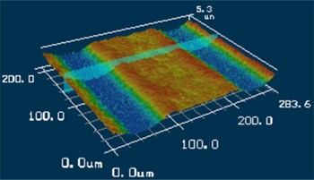
In this section, we present an example of a coplanar transmission line with loss characteristics that are complex to characterize. Figure 1 shows a three-dimensional (3D) image of a coplanar transmission line segment printed using a modern printing process and Fig. 2 shows a photograph of the same structure. From the 3D image, one can see the roughness pattern on top of the signal conductor, the center conductor section. The plane that is highlighted over the cross section was the location where the transmission line dimensions and surface roughness characteristics were measured in Fig. 3.

Fig. 1. 3D image of a coplanar transmission line.

Fig. 2. Photograph of a coplanar transmission line.

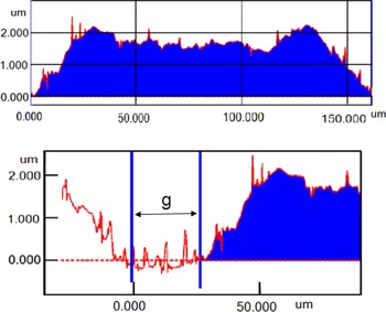
Fig. 3. Cross-sectional profile measurements of a coplanar transmission line, signal conductor (above), and coplanar gap (below).
For the fabrication of these transmission lines, a dispersion of nanoscaled silver particles was printed on a glass substrate with a CAD driven, mask less Aerosol Jet® printer from Optomec Inc. For this purpose, the dispersion was transferred to an aerosol stream by use of an ultrasonic source and then deposited on the substrate by a focused beam. Structures resulted in small line widths of 25 µm and sharp edge definition. The lines were sintered afterwards in a convection furnace at 250°C for 120 min. This maskless deposition technique is valuable for rapid prototyping applications, e.g. for printed antennas, embedded passives and sensor structures, respectively (see e.g. [Reference Zöllmer19]).
The DC resistance of the transmission line is dependent on the cross-sectional area of the signal conductor. Figure 3(top) is a profile measurement of the signal line and Fig. 3(bottom) is a profile measurement of the coplanar gap. The surface roughness of the conductor penetrates a significant amount into the surface of the conductor in comparison to the thickness of the conductor. In this case, the surface roughness will also play a role at low frequencies and the impact will increase to the high-frequency range. Because the surface roughness is 3D, the average cross-sectional area cannot be known from a single profile measurement and can only be assumed to be similar to that of the single cross-sectional profile. In the 3D image in Fig. 1, the roughness appears relatively uniform in the z-direction. Also, because the line is much wider than the root mean square (RMS) roughness height, we will assume that the longitudinal direction has similar roughness characteristics to the lateral direction. At high frequencies, as the skin effect decreases to a similar height as the surface roughness, the current must meander through the peaks and valleys of the roughness, increasing the resistance further. The edges of the conductors are very narrow angles – which are referred to as edge effects in this paper. This is further complicated by a strong proximity effect, as a result of adjacent conductors, that draws the current further into the edge of the conductor. As the frequency increases, the surface roughness effect will not only increase due to skin effect, the proximity effect and edge-effects will also have an impact on its behavior. Furthermore, the surface roughness on the return current paths must also be analyzed, because the proximity effects and edge effects will cause current crowding on the reference conductors.
Figure 4 shows scanning electron microscope (SEM) photos of sintered and unsintered printed conductors. The structure in Fig. 1, for example, is after sintering. This highlights another challenge of surface roughness modeling. The fabrication, as well as treatments after fabrication, can have a strong effect on the RMS roughness height and the form and constitution of the metalization. In some cases, the RMS height is not the only characteristic that could be used to characterize the roughness.

Fig. 4. SEM images of unsintered silver conductor (left) and sintered silver conductor (right).
V. A FILAMENT MODEL ADAPTED FOR PROXIMITY, EDGE, AND SURFACE ROUGHNESS EFFECT
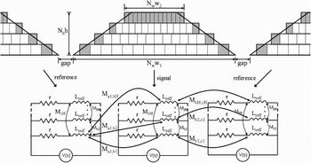
Filament models are commonly used to calculate the resistance and inductance of a conductor. The VuDinh model [Reference Vu Dinh, Cabon and Chilo5] is easily programmed and can quickly solve for the skin effect in a rectangular conductor cross section. Referring to Fig. 5(top), the cross section of a trapezoidal conductor is discretized and resistances, inductances, and mutual inductances are calculated for each filament (a modification of the VuDinh model). The same is done for the reference conductors, in this case the two coplanar flanks. Three different ladder circuits are constructed for the three different conductors as in Fig. 5(bottom). Then, a mutual inductance matrix between each reference conductor and the signal conductor is created containing the mutual inductances between every filament in each conductor.

Fig. 5. Diagram of a filament model and its corresponding ladder circuit.
The mutual inductance was calculated with equation (2) published in [Reference Weeks, Wu, McAllister and Singh7]. The same equation is used to determine the mutual inductances between the filaments in the different conductors. The self-inductances of the filaments were calculated with equation (1) presented in [Reference Mei, Amin and Ismail9]. The resistances were calculated with the traditional formula for the resistance of a prism, equation (3). In equations (1)–(3), l, w, and h are the length, width, and height of a filament, respectively. The variable r is the distance between the center points of two filaments.
![M=0.2l\left[{\ln \left({\displaystyle{l \over r}+\sqrt {1+\displaystyle{{l^2 } \over {r^2 }}} } \right)- \sqrt {1+\displaystyle{{r^2 } \over {l^2 }}}+\displaystyle{r \over l}} \right]\mu H\comma \;](https://static.cambridge.org/binary/version/id/urn:cambridge.org:id:binary:20151022073210862-0850:S1759078710000450_eqn2.gif?pub-status=live)
The adapted filament model proposed in this paper is based on the VuDinh model. The extensions that have been applied to the VuDinh model are outlined in this section. For the adapted filament model, to directly account for surface roughness, this resistance value is altered. In our case, to account for the surface roughness of the conductor, the resistances of the outside filaments (for example, the filaments shaded in Fig. 5(top)) were increased. A systematic approach for selecting the resistance of filaments has been implemented in the model. This leaves us with signal and reference conductors with inhomogeneous conductivities over their cross sections. The model is then solved with a computer, using equation (4). In equation (4), V x and I x are 1 × N T voltage and current vectors of each filament in conductor X, where N T = N w × N h (N w and N h are the number of horizontal and vertical filaments, shown in Fig. 5). Matrixes r x are N T × N T square diagonal matrixes, where the diagonal value in each row represents the resistance of a filament. Matrixes L x are N T × N T inductance matrices, where each row and column represent a specific filament and the matrix values are the mutual inductances between the filaments for that row and column. For the diagonal values, where the row and column represent the same filament, the value is the self-inductance. M x,Y are N T × N T matrices, where each row is a filament from conductor X and each column is a conductor from conductor Y and each element corresponds to the mutual inductance between the two filaments. The term s is the Laplace variable
![\eqalignno{&\left[\matrix{V_{{\rm Re} f1} \hfill \cr V_{Signal} \hfill \cr V_{{\rm Re} f2}} \right] = \left[\left[\matrix{r_{{\rm Re} f1} \hfill &0 \hfill &0 \hfill \cr 0 \hfill & r_{Signal} \hfill & 0 \hfill \cr 0 \hfill & 0 \hfill & r_{{\rm Re} f2} \hfill} \right] \right. \cr &\quad \left. + s \left[\matrix{L_{{\rm Re} f1} \hfill & M_{{\rm Re} f1\comma Signal} \hfill & M_{{\rm Re} f1\comma {\rm Re} f2} \hfill \cr M^T_{{\rm Re} f1\comma Signal} \hfill & L_{Signal} \hfill & M_{Signal\comma {\rm Re} f2} \hfill \cr M^T_{{\rm Re} f1\comma {\rm Re} f2} \hfill & M^T_{{\rm Re} f2\comma Signal} \hfill & L_{{\rm Re} f2} \hfill} \right] \right] \cr &\quad \times \left[\matrix{I_{{\rm Re} f1} \hfill \cr I_{Signal} \hfill \cr I_{{\rm Re} f2}} \right].}](https://static.cambridge.org/binary/version/id/urn:cambridge.org:id:binary:20151022073210862-0850:S1759078710000450_eqn4.gif?pub-status=live)
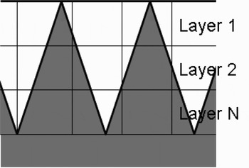
Figure 6 is a view of the surface filaments with surface roughness. The resistances of the filaments can be modified based on a specific technology – for example, a different resistance gradient could be developed for each profile in Fig. 4 based on measurements (this “technology specific” approach is valuable when the roughness shape is very unique). For standard applications, to approximate a nearly regular sawtooth roughness pattern, the resistance of the filaments in the region of surface roughness is increased in an exponential gradient (exponential to reflect both the horizontal and linear dimensions of the roughness). This concept is similar to the traditional Hammerstad surface roughness model, which assigns essentially a frequency-dependent effective conductivity to the conductor. With the adapted filament model, however, the effective resistance is only applied to the part of the conductor with surface roughness. Then, the conductivity gradient stays constant over the frequency range, while the current density in the conductor changes. As the current migrates to the outside, the higher resistance filaments, representing surface roughness, cause the resistance to increase above the ideal value. The surface roughness heights can be applied at random (with a random number generator) to each column of filaments to approximate random surface roughness with an average height. However, for a large number of filaments, this technique will average out to approximately the same as a constant resistance gradient. Therefore, a set of equations was developed to find the effective resistance of the filaments as a function of the layer in which they are located.

Fig. 6. Cross-sectional areas of the filaments for different surface roughness profiles.
The approximation is made such that the surface roughness penetrates uniformly across the surface, with RMS peak-to-peak height of the surface roughness, as it does in Fig. 6. The following equations, equations (5) and (6), describe what resistance the filaments were assigned. The variable K FIL(n) is the coefficient that determines the resistance of the filament. The variable N is the total number of layers that the peak-to-peak RMS surface roughness height penetrates, or the quotient of the surface roughness height (H SR) and the filament height. For example, in the drawing in Fig. 6, the N = 3. The variable n is the layer that the filament occupies, starting with n = 1 at the layer on the surface, and increasing inward, until the average roughness height is reached. R FIL,EFF is then the effective resistance of the particular filament. In equation (6), l, w, and h are the length, width, and height, respectively, of an individual filament, making the numerator of equation (6) the resistance of an individual filament.

The model will compute DC effects of surface roughness and the bandwidth should continue to the point where the skin-depth is approximately equal to the height of the discretized filaments.
VI. VALIDATION OF THE ADAPTED SKIN-EFFECT MODEL
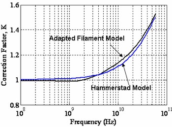
The first method used to validate the proposed model is to compare this to a traditional surface roughness model. This is only possible when we impose the limitations of the traditional model onto the proposed model. This means that (1) the models are compared for a transmission line with heterogeneous roughness; (2) the results are normalized by subtracting the DC difference so that no DC effects are included; (3) no proximity effects are included; and (4) no return current path is included. These limitations are imposed because the traditional surface roughness models are limited and we hope to make a fair comparison between our model and the traditional models. Essentially, we use the adapted filament model to model a conductor prism with a homogeneous surface roughness profile across the entire cross-section – an unrealistic case and valuable only as a comparison. The conductor, 10 µm wide and 5 µm thick copper, is simulated with and without roughness (0.45 µm RMS roughness height). To remove the DC effects in the adapted filament model, the results are scaled down by subtracting the small DC difference (which will cause no significant deviations at high frequencies) before dividing the curve with roughness by the curve without roughness. Figure 7 shows the similarity. The two correction factors vary by less than 10% across the entire frequency range.

Fig. 7. Comparison of the Hammerstad and adapted filament models for surface roughness modeling.
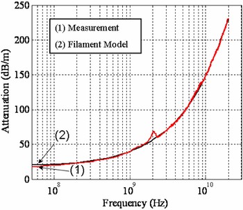
But, to accurately validate the adapted filament model, because it is a much different technique than state-of-the-art methods, it must be compared with measurements. So, the adapted model was then used to model the transmission line in Fig. 1. The width of the line in the model was w = 165 µm, the average thickness was t = 1.7 µm, the gap distance was g = 25 µm, the modeled surface roughness on the top and angled surfaces was on an average of 0.25 µm, and the surface roughness of the bottom surface was zero (the dimensions are also shown in Fig. 3). The bottom surface roughness was assumed to be the roughness of the glass substrate, which, with a separate measurement was less than 20 nm (smaller than the capabilities of the measurement equipment). The roughness in the gap in Fig. 3 is from overspray of nanopartical agglomerates, any effects of which are neglected. The measured surface roughness height was 0.22 µm RMS. The length of the measured line was l = 15 mm. The conductivity of the metallic ink was σ = 2.5 × 10⁷ S/m, in the range of what the manufacturer specifies, but was determined by matching the lowest frequencies in the model and measurements (considered the quasi-DC case). The lower angles of the conductor trapezoids were 4.8°, which was calculated from the profile measurements (Fig. 3). The characteristic impedance was determined analytically to extract the attenuation from S-parameter measurements. In Fig. 8, the measurement was compared to the results of the model. The computation was done with a Matlab program and took approximately 20 min.

Fig. 8. Modeling and measurement results.
The structure was built on a glass dielectric. Considering the dielectric loss tangent, tan(δ), is 0.001, then based on a quick analytical estimate, from equation (7) (where q is the filling factor, λg is the guide wavelength, and tan(δ)) is the dielectric loss tangent) the dielectric losses will be less than 3 dB/m at 20 GHz [Reference Wadell20]. The substrate losses then compose less than 2% of the overall losses. For this reason, they are neglected during the following calculations:
Measurements were conducted of the transmission line in Fig. 1 with a vector network analyzer. A curve moving average program was used after the measurement. Accuracy of the model at high frequencies can be improved by increasing the discretization. The measurements show an agreement with the analytical results using the filament model. Over the entire frequency range, the average error is less than 2%, with the exception of the resonance in the measurement at 2 GHz.
Often in full-wave simulations, surface roughness is accounted for using the Hammerstad correction factor [Reference Curran, Ndip, Guttowski and Reichl11], equation (8), where Δ is the RMS height of the surface roughness and δ is the skin-depth. This would be applied to the surface resistivity of the conductor:

The transmission line used during this validation is unique, because the skin-depth is first equal to half the conductor thickness around 15 GHz but roughness has an effect starting around 2 GHz. This means that an accurate full-wave simulation should generate a mesh inside the conductor because the resistance will not be accurately computed for the lower frequencies. Generating a mesh inside the conductor, for a transmission line of this size and width to height ratio, will drastically increase computation times. This complicates the state-of-the-art approach of applying a correction factor to the surface resistivity during a full-wave simulation. Full-wave simulations also do not offer physical insight into the source of losses.
VII. ACCOUNTING FOR THE SOURCE OF CONDUCTOR LOSSES WITH THE ADAPTED FILAMENT MODEL
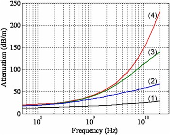
Using the filament model, one can determine the source of the different losses. By eliminating the reference planes, the surface roughness correction, and the trapezoid angles, the attenuations as a result of a skin effect in an ideal conductor is determined. Adding the reference conductors the impact of the proximity effect is demonstrated (an ideal coplanar transmission line). Then the angles are added to the conductors to determine the impact of edge-effect on the losses. Then, finally, the adapted filament model is used. This breakdown of losses is shown in Fig. 9. The edge-effects begin to have an effect starting around 500 MHz and the surface roughness effect around 2 GHz. At 20 GHz, the modeled losses, with the non-idealities included, exceed the ideal rectangular coplanar transmission line by more than 300%. This breakdown offers an additional advantage over traditional methods because the modeling can also be applied during the characterization phase of a transmission line to examine the magnitude and frequency ranges of different effects. This breakdown can also be used for optimization.

Fig. 9. Breakdown of losses in a coplanar line (1) skin effect in ideal copper slab, (2) skin effect and proximity effect in an ideal coplanar line, (3) skin effect and proximity effect in a coplanar line with angled edges, and (4) a trapezoidal coplanar line with surface roughness.
VIII. CONCLUSION
In this paper, a coplanar transmission line is modeled using a filament model. The filament model is similar to state-of-the-art filament models that discretize a conductor cross section and adjacent reference conductor cross sections and solve for the per unit length resistance. Advancement beyond the state-of-the-art filament model is made as it is adjusted to account for the trapezoidal cross-section and surface roughness of the conductors. This model accurately predicted the response of the conductor and offered a physical insight into the source of the losses that was not given with full-wave simulations. It has been shown why special attention to the proximity effect was necessary for understanding its impact. Also, a model that accounts for the surface roughness effects from DC through the skin-effect corner frequency, where the surface roughness height is the same as the skin-depth, δ, and into high frequencies will give better results than the traditional analytical surface roughness models.
The improved model shows various improvements over state-of-the-art techniques. It offers improved accuracy than analytical solutions and faster computations than full-wave simulations. Additionally, the new model has also been able to divide the different loss mechanisms to better understand the source of the losses in a particular transmission line.
 Brian Curran (M'09) received a B.S. degree in electrical engineering from the University of Rochester, New York, in 2001 and an M.S. degree in electrical communications engineering from the University of Kassel, Germany, in 2008. He is currently working toward a doctoral degree at Fraunhofer Institute for Reliability and Microintegration (IZM) in Berlin. His main research interest is interconnect modeling.
 Ivan Ndip (M'05) studied electrical engineering at the Technische Universität (TU) Berlin, Germany. He obtained his M.Sc. (Dipl.-Ing.) and Ph.D. (Dr.-Ing.) with the highest distinction (Summa cum Laude) in 2002 and 2006, respectively. In 2002, he joined the Fraunhofer-Institute for Reliability and Microintegration (IZM) Berlin as a Research Engineer and worked on signal integrity modeling and design of system packages and boards as well as on antenna design and integration. Between 2003 and 2005, he was also affiliated with the Chair for High-Frequency Electronics at the University of Paderborn. In 2005, he was appointed Group Manager. He developed novel concepts that led to the formation of a new research group at Fraunhofer IZM, the RF and High-Speed System Design Group, in February 2006. Since then, he has been leading this group, where he is responsible for developing and leading research projects that focus on modeling, design and optimization of RF/high-speed modules, integrated antennas, and passive RF front-end components. Since 2008, he has also been a lecturer in the Department of High-Frequency and Semiconductor System Technologies, School of Electrical Engineering and Computer Sciences, Technische Universität Berlin. He developed and is currently teaching graduates on the application of electromagnetic field theory for high-frequency design and measurement of electronic packaging and system-integration structures. Dr. Ndip has more than 70 publications and has won five best paper awards at leading international conferences. He is also a recipient of the Tiburtius-Prize, awarded yearly for outstanding Ph.D. dissertations in the state of Berlin, Germany. He co-chairs the signal and power integrity subcommittee of the International Microelectronic and Packaging Society (IMAPS). He is also a member of the European Microwave Association (EuMA) and the German Association for Electrical, Electronic and Information Technologies (VDE). Dr. Ndip is serving as a reviewer for many international journals among which includes three IEEE Transactions (Computer-Aided Design of Integrated Circuits and Systems, Electromagnetic Compatibility, and Electronics Packaging Manufacturing), Journal on the Progress in Electromagnetics Research (PIER), Wiley International Journal of Numerical Modeling: Electronics Networks, Devices and Fields, and the Electronic Letters of the Institution of Engineering and Technology (IET). He also serves on the Technical Program Committee of the Electrical Design of Advanced Package and Systems Symposium (EDAPS), the Asia-Pacific EMC Symposium (APEMC), and the International Symposium on Microelectronics.
 Christian Werner received a Diploma degree in industrial engineering and management from the University of Bremen in 2007. He is now a project manager at the Fraunhofer Institute for Manufacturing Technology and Applied Materials. His main research focuses on surface functionalization by printing techniques.
 Veronika Ruttkowski studied chemical engineering with focus on analytics at the University of Applied Sciences in Lübeck, Germany and received her diploma in February 2006. Since January 2007 she is working at Fraunhofer IFAM in Bremen as Project Manager.
 Marcus Maiwald studied electrical engineering with focus on micro system technology at the University of Bremen, Germany. In 2006, he received his diploma and joined the Fraunhofer Institute for Manufacturing Technology and Applied Materials Research in Bremen as Project Manager. He currently studies the development of sensor structures by printing technologies.
 Heinrich Wolf received his Diploma degree in Electrical Engineering from the Technical University of Munich (TUM) and his Ph.D. from the Technical University of Berlin, Germany. He joined the Chair of Integrated Circuits at the TUM as a member of the scientific staff working on Electrostatic Discharge (ESD) related issues. This involved modeling of ESD-protection elements, parameter extraction techniques, and test chip design. In 1999, he joined the Fraunhofer-Institute for Reliability and Microintegration (IZM). He was involved in the investigation of ESD phenomena for CMOS and Smart Power Technologies. Furthermore, he published on the development of ESD test methods and tester characterization. Currently, he is coordinating the ESD related activities at the IZM and also working on the field of RF transmission line design.
 Dr. Volker Zöllmer studied Chemistry and Mineralogy at University of Kiel. He got his Diploma degree as Mineralogist in 1999. In 2002, he finished his Ph.D. at University of Kiel, Germany. Based on his Ph.D. work, he received the award “DGM-Nachwuchspreis 2002” from the “Deutsche Gesellschaft für Materialkunde (DGM)”. In April 2002, he moved to Fraunhofer-IFAM, Bremen, Germany, and became a Project Manager for the development of metallic foams. Since 2003, he heads the Department of “Functional Structures” at Fraunhofer-IFAM. His main research areas are the development of nano-porous structures, nano-particles, and nano-scaled suspensions. He established the technology platform “INKtelligent printing®” for a customized functionalization of components and surfaces. Dr. Zöllmer is heading several industrial projects and his department “functional structures” is involved in national and international research projects focusing on rapid prototyping, functional integration, and surface structuring.
 Gerhard Domann studied physics in Heidelberg and Oldenburg, Germany and graduated in 2001. Since 2001, he works at Fraunhofer ISC. The main focus of his work is the development and the processing of inorganic–organic hybrid polymers applicable in micro-systems (micro-optic, micro-electronic, etc.). The development of dielectrics and encapsulation materials based on this material class, which can be patterned by maskless processes such as ink-jet printing is part of these research activities. Since 2008, he holds an MBA from TiasNimbas, NL.
 Stephan Guttowski obtained his M.Sc. (Dipl.-Ing.) degree in electrical engineering from the TU Berlin in 1994 and his Ph.D. (Dr.-Ing.) degree in 1998. From 1998 to 1999, he worked as a Post Doctoral Research Fellow at M.I.T., where he headed the research unit that explored the consequences of the new 42-V-Systems on the electromagnetic compatibility within future passenger cars. In 1999, he joined the Research Laboratory for Electric Drives at DaimlerChrysler AG in Berlin and was involved with the prediction of electromagnetic emission of electrically driven vehicles. Dr. Guttowski joined Fraunhofer IZM Berlin in October 2001. From 2002 to 2005, he headed the Advanced System Development Group. Since January 2006, he has been Head of the Department of System Design and Integration. He has extensively published in the area of electrical design of electronic packages and boards for high performance miniaturized systems.
 Dr. Horst A. Gieser is head of ATIS-Analysis and Test of Integrated Systems in the Polytronic Systems Department of the Fraunhofer-Institute for Reliability and Microintegration. He received his Diploma degree in electrical engineering and his Ph.D. from the Technical University of Munich. He has authored and co-authored more than 50 publications including two books mainly in the field of electrostatic discharge (ESD). Four of them were awarded at international conferences. Currently, he is chairing the ESD Forum e.V., a German non-profit association that supports the exchange of experience in this complex subject by means of a bi-annual symposium called ESD-Forum. He headed the Technical Program Committee of the EOS/ESD-Symposium 2007 and the International ESD-Workshop 2008. Further interests are in the field of device characterization with ultra-short transients and up to very high frequencies as well as the vertical integration of systems VSI®.
 Herbert Reichl (F'00) is the Director of the Fraunhofer IZM and a full Professor at the Technical University Berlin, Head of the Research Center for Microperipheric Technologies. He has published umpteen scientific papers individually and co-authored six books. He is a member of the European High Level Expert Group of the Nanoelectronics Platform (ENIAC), board member of EUREKA Industrial Initiative for Microsystems Uses (EURIMUS), and a member of the Scientific Committee MEDEA.
Professor Reichl was awarded with the Order of Merit of the Federal Republic of Germany, in 2000. For his eminent contribution to research and development of Fraunhofer-Gesellschaft, he was honored with the highest award of Fraunhofer-Gesellschaft, the “Fraunhofer Muenze” in 2005. The IEEE Components, Packaging and Manufacturing Technology Society awarded him with a Special Presidential Recognition in recognition of his lifetime of technical achievement in microelectronics as a scholar, mentor, and global leader. He was given the iNEMI International Recognition Award in 2005. In 2006, he received the highest VDE award and in 2007 he was honored with the Electronics Manufacturing Technology Award.