I. INTRODUCTION
As one of the important III–V semiconductors, AlN has wide applications in field emission, high-power, and high-frequency electronic devices owing to unique properties such as high thermal conductivity, good electrical resistance, low dielectric loss, and ideal thermal expansion (Monemar, Reference Monemar1999; Han et al., Reference Han, Jin, Zhang, Tang, Li, Liu, Liu, Lei and Zhou2004). Among the III-nitride compounds, AlN exhibits the largest direct band gap (6.2 eV) and the shortest wavelength ultraviolet emission near the band gap. This makes AlN an ideal material for fabricating short wave light-emitting diode (LED) as the solid-state light sources (Morkoç et al., Reference Morkoç, Strite, Gao, Lin, Sverdlov and Burns1994), which has been regarded as an excellent alternative to replace the conventional lighting sources such as gas lasers and mercury lamps. Compared with the AlN bulks, one-dimensional (1D) structured AlN has a compact size and a high aspect ratio, making AlN exhibit a much better performance in field emission, reinforcement in ceramic-matrix composites, and potential applications for nano scaled optoelectronic devices (Tang et al., Reference Tang, Cong and Cheng2007; Liu et al., Reference Liu, Su, Mo, Li, Chen, Liu, Chen, Deng and Xu2011). Therefore, the synthesis of high purity 1D structured AlN is of particular interest.
Quasi-1D AlN whiskers or nanowires have been produced by different methods including carbothermal reaction of aluminum oxide (Jung and Joo, Reference Jung and Joo2005), direct nitridation of aluminum powder (Liu et al., Reference Liu, Bando, Wu, Jiang, Dierre, Sekiguchi, Tang, Mitome and Golberg2010), chemical vapor deposition (Wu and Liang, Reference Wu and Liang2009), and silica-assisted catalytic growth method (Tang et al., Reference Tang, Fan, Chapelle and Li2001). Generally, the prepared 1D AlN often exhibit different photoluminescence (PL) characterizations. A wide emission band ranging from 600 to 400 nm centered at 426 nm was observed by Lei et al. (Reference Lei, Yang, Guo, Song, Li and Tang2007). They reported that oxygen impurity was a key factor leading to the wide blue band, and a similar phenomenon was also observed by Xu et al. (Reference Xu, Xue, Yin and Wang2003). Byeun et al. (Reference Byeun, Telle, Jung, Choi and Hwang2010) reported the band with a maximum at 500 nm from the 1D single-crystalline AlN nanostructures and the emission band was attributed to the vacancy of Al or O impurity. PL spectrum of AlN whiskers was composed of two emission bands located at 405 and 510 nm, attributed to the nitrogen vacancy, was reported by Jiang et al. (Reference Jiang, Zuo, Wang, Li, Jin, Wang and Chen2011). Recently, Li et al. (Reference Li, Song, Wu, Li and Jian2012) reported a sharp ultraviolet emission at 358 nm from well-aligned wurtzite-structured AlN nanorods. Summing up from the former studies, it is still a challenge to achieve ultraviolet emission approaching the band gap in 1D AlN nanostructures because of O impurity, vacancy defects, and excessive surface defects.
In this study, high-quality crystalline AlN whiskers with ultraviolet emission at 345 nm were produced by PVT method. This method has advantages of high yield, low contamination, and the diameter or length of the whiskers can be easily controlled (Bao et al., Reference Bao, Chen, Li, Wang, Song and Wang2009). To the best of our knowledge, the 345-nm emission is the shortest wavelength observed in 1D AlN materials. This ultraviolet emission will make AlN whiskers a more promising material in AlN-based nanodevices, especially solid-state lighting source, ultraviolet LED, and lasers.
II. EXPERIMENTAL
The growth of AlN whiskers was achieved by the physical vapor transport (PVT) method in a radio frequency (RF)-heated furnace capable of maintaining a temperature of up to 2400 °C. High-purity AlN (99.9%) powder was used as the reactant source. The source was first placed into the TaC crucible loaded in a graphite crucible, then the graphite crucible was placed inside the induction heating furnace. A sketch of the experimental configuration of the crucible and growth assembly was illustrated by Zuo et al. (Reference Zuo, Wang, Chen, Jin, Jiang, Bao, Guo, Wei and Wang2012). AlN whiskers were grown in a temperature of 1800 °C, under a nitrogen (99.99%) pressure of 0.6 atm and a distance of 15 mm between the source and crucible lid. After 6 h growth, large quantities of white AlN whiskers were deposited on the TaC lid. Crystalline phase identifications were performed on an X-ray diffractometer (X'Pert ProMRD) with CuKα radiation at 40 kV and 40 mA. The composition of the samples was determined from X-ray photoelectron spectra (XPS), which was recorded on an X-ray photoelectron spectrometer, using monochromatized Al X-rays as the excitation source. The morphologies and microstructures of the samples were observed by a scanning electron microscope (SEM, FEI, XL-30) and a high-resolution transmission electron microscope (HRTEM, JEOL, JEM-2010), respectively. Raman scattering measurement was performed at room temperature by a Raman system (JY-HR800) using the 532-nm line of a solid-state laser as an excitation source. PL spectra were conducted at room temperature with a Hitachi F-7000 spectrofluorometer using an Xe lamp as an excitation light source.
III. RESULTS AND DISCUSSION
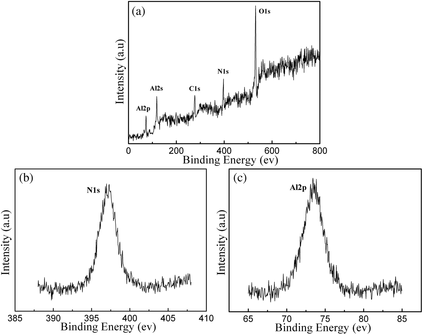
Figure 1 presents the photograph and a typical X-ray diffraction (XRD) pattern of the as-prepared samples. Large quantities of cotton-like white wires are deposited on the TaC lid. XRD diffraction peaks with miller indexes marked above can be indexed as hexagonal AlN (a = 3.114 Å and c = 4.981 Å), agreeing well with the standard reference diffraction pattern (ICDD-PDF No. 25-1133). In addition, no characteristic peaks of impurities such as Al2O3, AlON, and other compounds were found. XPS was applied to determine the element composition and corresponding chemical states of the sample. Figure 2(a) shows the measured spectrum of the sample, indicating the presence of elements Al, N, C, and O. The presence of carbon might have come from the sample handling and the oxygen may arise from the AlN surface oxidized layer when exposed to the atmosphere. No other impurity elements were detected in the XPS resolution limitation. The binding energies of N1S and Al2p centered at 396.5 and 73.5 eV, as shown in Figures 2(b) and 2(c), respectively, are in good agreement with the values of aluminum nitride films deposited by plasma source molecular beam epitaxy (Rosenberger et al., Reference Rosenberger, Baird, Cullen, Auner and Shreve2008). The Al2p is assigned to aluminum bound to nitrogen and the N1s is assigned to nitrogen bound to aluminum in wurtzite AlN.

Figure 1. Typical XRD pattern of an as-prepared sample, and the insert gives the photograph of the sample.

Figure 2. XPS spectra of an as-prepared sample: (a) survey spectrum, (b) N1s region, centered at 396.5 eV, and (c) Al2p region, centered at 73.5 eV.
SEM images of the as-prepared sample with different magnifications are shown in Figure 3. An overview of the samples [Figure 3(a)] reveals that ultra-long AlN whiskers with length up to several millimeters were obtained. The AlN whiskers are about 10–100 times longer than those previously reported (Wu and Liang, 2009; Liu et al., Reference Liu, Bando, Wu, Jiang, Dierre, Sekiguchi, Tang, Mitome and Golberg2010), and this ultra-long length will benefit tailoring and processing of the whiskers in electronic device applications. SEM image with higher magnification [Figure 3(b)] shows that the AlN whiskers are 1–3 µm in diameter, and exhibit smooth surface and good toughness. SEM image of a single AlN whisker with smooth surface and six-sided prismatic morphology is presented as an insert in Figure 3(b). From the six-sided prismatic morphology, one can deduce the AlN whiskers belonging to the hexagonal phase, and this agrees well with the XRD analysis. No liquid droplets can be found at the tip, indicating that the growth mode does not involve the vapor–liquid–solid (VLS) mechanism, but rather direct growth from the vapor phase (VS mechanism).

Figure 3. (a) Low-magnification SEM image of AlN whiskers with the length up to several millimeters, and (b) high-magnification SEM image of the AlN whiskers.
In order to determine the microstructure of AlN whiskers, TEM and HRTEM images were conducted. From the corresponding HRTEM image [Figure 4(a)], it can be seen that the AlN whisker exhibits a typical crystalline characteristic and is structurally uniform with clear lattice fringes, no defects such as dislocation or stacking faults are found. The insert magnified fringe of the HRTEM shows the interplanar spacing of the AlN lattice planes to be 0.249 nm, which agrees well with the d-spacing of the (002) lattice planes of hexagonal AlN, confirming that the [0001] direction is the preferred growth direction of the AlN whiskers. The selected area electron diffraction (SAED) pattern of the whisker is presented in Figure 4(b), confirming that the whisker grows along the [0001] direction. Previous work also reported that the AlN nanofibers grown by the sublimation method grew along the [0001] direction (Jiang et al., Reference Jiang, Zuo, Wang, Li, Jin, Wang and Chen2011).

Figure 4. (a) HRTEM image of an AlN whisker, the insert is magnified fringes of the HRTEM. (b) SAED pattern of the AlN whisker.
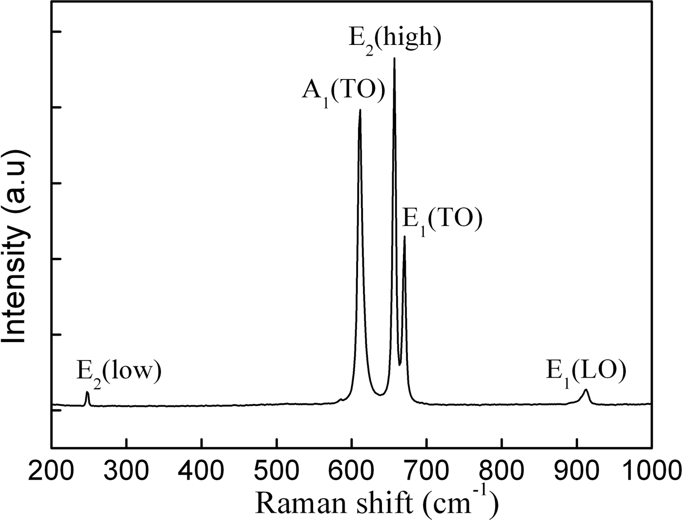
The structural information of the AlN whiskers was also investigated by backscattering geometry Raman spectra, which was recorded at room temperature using a 532-nm solid-state laser as excitation source. Since the space group of wurtzite AlN is P63 mc with all of the atoms occupying the C3V sites, six first-order Raman active modes may be present: A1(TO), A1(LO), E1(TO), E1(LO), E2(high), and E2(low) (Harima, Reference Harima2002). In the Raman spectrum in Figure 5, two high-intensity peaks at 656.3 and 610.5 cm−1 are indexed to the E2(high) and A1(TO) phonon modes, respectively. The peak at 670.5 cm−1 is indexed to E1(TO), whereas the two low-intensity peaks at 247.3 and 911.0 cm−1 are assigned to the E2(low) and E1(LO), respectively. It is also found that there are small shifts of about 2 cm−1 to the lower wavenumbers (red shift) for A1(TO), E2(high), and E1(TO) modes compared with the narrow peaks from bulk AlN data (Davydov et al., Reference Davydov, Kitaev, Goncharuk, Smirnov, Graul, Semchinova, Uffmann, Smirnov and Mirgorodsky1998). Red-shift phenomenon is commonly observed in some AlN nanowire (Xu et al., Reference Xu, Xue, Yin and Wang2003), nanobelt (Wu et al., Reference Wu, Hu, Wang and Chen2003), and nano particle structures (Lan et al., Reference Lan, Chen, Cao, Xu, Xun, Xu and Liang1999; Cao et al., Reference Cao, Chen, Lan, Li, Xu, Xu, Liu and Liang2000), as a result of decreasing microcrystal and impurity incorporation or the size confinement effect (Hayes et al., Reference Hayes, Kuball, Shi and Edgar2000). The size confinement effect may be impossible for shift of the Raman frequency because the diameter of the AlN whiskers studied here are approaching micrometers size. Meanwhile, blue-shift of phonon frequencies of AlN nanowires was observed in other work because of the compressive stress in the lattice (Zhao et al., Reference Zhao, Zhang, Xu, Wang, Xu, Yu, Li and Su2005). It is well known that impurities or stress in semiconductors significantly affect the Raman line width. The full-width at half-maximum of the A1(TO) and E2(high) are 7.9 and 7.0 cm−1, respectively, which are a little larger than those of the AlN crystallite (Bergman et al., Reference Bergman, Alexson, Murphy, Nemanich, Dutta, Stroscio, Balkas, Shin and Davis1999), indicating low concentration of impurities and stress in the whiskers. In our study, the narrow Raman peaks with a less shift indicate a good crystalline quality and homogeneous structures of AlN whiskers were obtained.

Figure 5. Raman scattering spectrum of AlN whiskers.
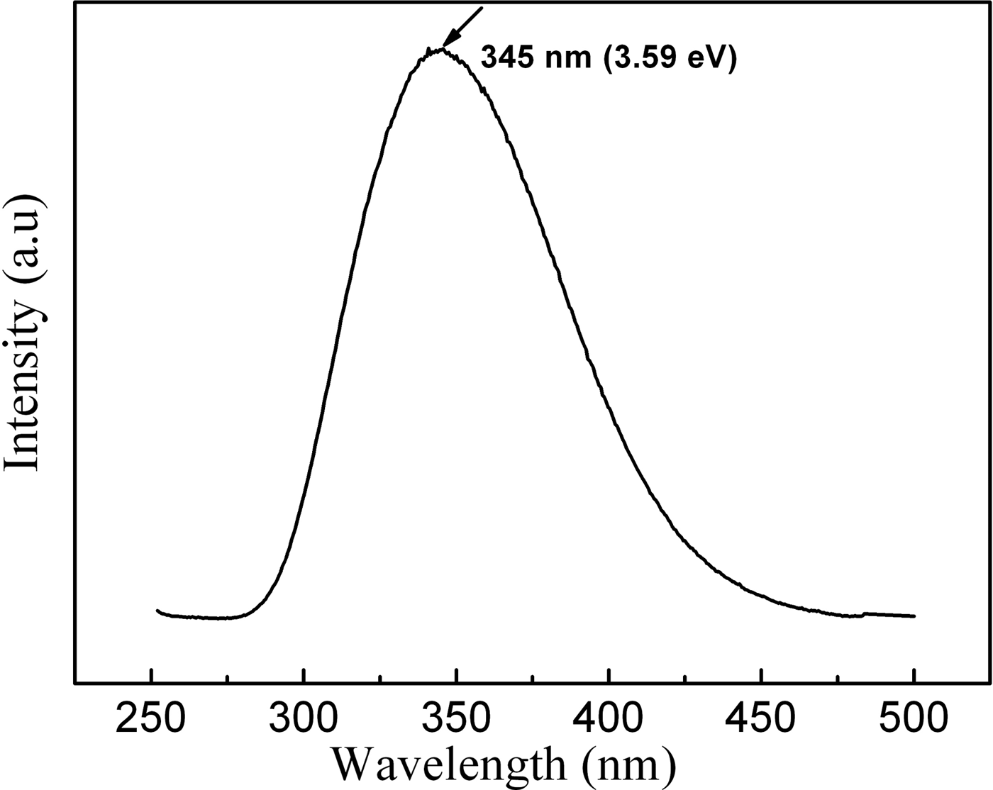
PL measurements were conducted at room temperature at an excitation wavelength of 260 nm by using Xe lamp as the light source. As shown in the PL spectrum Figure 6, one can only observe a strong ultraviolet emission peak centered at 345 nm (3.59 eV), which is even 7 nm shorter than the shortest ultraviolet emissions of the AlN whiskers reported by Liu et al. (Reference Liu, Bando, Wu, Jiang, Dierre, Sekiguchi, Tang, Mitome and Golberg2010). The luminescence properties of AlN had been extensively studied in the past couple of decades and diverse luminescence mechanisms had been reported. Generally, nitrogen deficiency, aluminum vacancy, and oxygen point defect were deemed to be the origin of the luminescence below band gap (Slack, Reference Slack1973; Youngman et al., Reference Youngman, Harris and Chernoff1989; Berzina et al., Reference Berzina, Trinkler, Sils and Atobe2002; Schulz et al., Reference Schulz, Albrecht, Irmscher, Hartmann, Wollweber and Fornari2011). Liu et al. (Reference Liu, Bando, Wu, Jiang, Dierre, Sekiguchi, Tang, Mitome and Golberg2010) pointed out that the UV emission (352 nm) of the AlN whiskers could be attributed to the transition between the deep impurity center (oxygen) and the valence band. Youngman et al. (Reference Youngman, Harris and Chernoff1989) ascribed the broad band at 2.7 eV (457 nm) and 3.8 eV (326 nm) from AlN single crystals grown under nitrogen-deficient conditions results from the vacancy of N (VN). Schulz et al. (Reference Schulz, Albrecht, Irmscher, Hartmann, Wollweber and Fornari2011) investigated the optical properties in insulating, irradiation damaged bulk AlN crystals. An isolated transition, peaking about 3.3 eV (376 nm) was attributed to a donor–acceptor pair transition involving an unknown shallow donor and the isolated Al vacancy. Slack (Reference Slack1973) reported that the formation of ON (oxygen occupies a regular N site) accompanied by VAl for charge compensation. Thus, a state related to ON–VAl complex is formed inside the AlN band gap with a probable excited state close to the conduction band. According to the energy scheme proposed by Berzina et al. (Reference Berzina, Trinkler, Sils and Atobe2002), the ON–VAl complex level locates at about 1.2 eV above the valence band and the separated ON ion level locates at about 4.3 eV. High-purity AlN source and nitrogen gas were used to grow AlN whiskers. Although some residual oxygen in the chamber would dissolve into the AlN lattice because of the high chemical affinity of aluminum and oxygen, the concentration oxygen in our sample is very low. Therefore, the emission at 345 nm (3.59 eV) could not be attributed to the ON level or the ON–VAl complex level. It might be attributed to VN. The oxygen element originating from surface absorption may also contribute to the emission. Of course, the exact PL mechanism of the AlN whiskers requires further investigation. Such a strong and uniform 345 nm ultraviolet emission will make the AlN whiskers ideal candidates for the application of ultraviolet optoelectronic nanodevices.

Figure 6. Room-temperature PL spectrum of AlN whiskers excited at 260 nm.
IV. CONCLUSION
Large quantities of ultra-long AlN whiskers were produced by the PVT method through the VS mechanism. The as-prepared samples were less contaminated by oxygen and well crystallized. A strong and uniform 345-nm ultraviolet emission has been realized in the AlN whiskers. This emission is attributed to VN and the surface defect states. Such extensive and uniform ultraviolet emission, as well as high crystal quality and ultra-long length, will make AlN whiskers ideal candidates for the application of nano- or micro devices in optoelectronics.
ACKNOWLEDGEMENTS
This work was supported by the National Natural Science Foundation of China (grant numbers 51210105026 and 51172270), the National Basic Research Program of China (973 Program, grant no. 2013CB932901), and Chinese Academy of Sciences.