I. INTRODUCTION
Today's low-cost technologies have driven the need to be able to test high volume complex microwave integrated circuits (ICs) at a fraction of the cost of the IC. However, usual testing techniques of microwave circuits are very expensive. The production test cost depends on two main factors: the time spent per tested parameter/circuit and the cost associated with the implementation and equipment used for the test [Reference Ferrario, Wolf and Moss1]. In order to minimize the overall test cost, new alternatives for microwave circuits have been investigated by means of design for test (DFT), built-in-self-test (BIST), and alternate test methods [Reference Ferrario, Wolf and Moss1–Reference Ryu, Kim and Sylla5].
In this particular context, this work deals with a new BIST solution to test the absolute gain, the compression point (CP1), and the bandwidth of a K-band satellite receiver (R x) for TV reception. As shown in Fig. 1(a), the radiofrequency (RF) BIST solution consists of injecting the RF input signal of the device under test (DUT) by using an integrated BIST generator and by measuring the output signal of the DUT converted to a DC signal with an RF detector. Both the BIST generator and RF detector are integrated on the DUT's chip. This paper focuses on the design of the RF generator, which is the most sensitive part of the BIST circuit. It is organized as follows: the circuit analysis and design are discussed in Section II and Section III deals with measurement results. A conclusion and perspectives are given in Section IV.

Fig. 1. (a) Concept of the proposed BIST approach and (b) frequency planning of the DUT.
II. CIRCUIT ANALYSIS AND DESIGN
A) Device under test
The DUT is a terrestrial satellite receiver composed of a low noise amplifier (LNA), a band-pass filter for image rejection, and a mixer (Fig. 1(a)). It contains three sub-bands (Fig. 1(b)). The typical conversion gain varies from 15 to 18 dB with a 1-dB input CP1 equal to −31 dBm. As this product has to be produced in very high volumes, therefore, the development of alternative methods that will reduce both the test time and cost is required.
B) BIST concept
The conversion gain and the CP1 being two critical parameters of the receiver, we have focused on the first approach on the design of a BIST circuit for the measurement of these parameters. In the literature [Reference Huang, Hsieh and Lu3–Reference Ryu, Kim and Sylla5], relative measurements are proposed. Usually, two RF detectors at the input and at the output of the DUT are used to convert the RF signal to a DC one. However, the approach proposed in this paper involves a single measurement at the output of the DUT. It consists of injecting the RF input signal of the DUT internally with an integrated generator and measuring the output of the DUT converted into a DC signal (Fig. 1(a)). This approach presents many advantages. It removes expensive external RF equipment, i.e. the RF source and spectrum analyzer. Consequently, this will also secure and standardize the industrial test. In addition, it will make the test easier and quicker because only a single DC measurement is required.
C) Requirements
The BIST generator is used to inject at the R x input an RF signal the frequency and amplitude of which are known. As it will not be remeasured in the industrial test, the BIST generator should be guaranteed by design to minimize the likelihood of being faulty compared to the DUT. The DUT has to fulfill requirements such as gain, linearity, consumption, etc., while the focus of the BIST circuit is its robustness against process variations and mismatches. Other parameters such as power consumption and phase noise were considered less important because the BIST circuit is activated only during the test operation. The frequency range of the BIST generator must cover at least that of the DUT, i.e. (18.2–22 GHz) with an accuracy better than ±2.5%. To be able to test the gain and the CP1 (=−31 dBm) of the DUT, the power range should vary at least between −40 and −28 dBm (at the input of the receiver) with an accuracy of ±1 dB, which is comparable to Automatic Test Equipment RF generators. The dynamic power and the frequency ranges of the BIST circuit have to be as large as possible so that the design could be reused for other types of applications.
The BIST circuit is implemented on the same chip as the DUT with the constraint to not degrade the R x functional performances, i.e. the noise figure, the gain, the return loss, etc.; therefore, it must be transparent and not intrusive in the normal operating mode. The output impedance of the BIST generator needs to be matched with the 50 Ω input impedance of the DUT. The circuit is designed with an NXP SiGe:C BiCMOS process (0.25 µm CMOS, 140 GHz Ft) [Reference Van Noort6].
C) Circuit architecture
The BIST generator consists of an LC voltage controlled oscillator (LC-VCO), a buffer to strengthen the isolation with the next blocks, and a variable controlled attenuator. For this first version of the circuit, in order to not degrade the RF performances of the DUT in normal mode, an external loopback via the probe card is used to connect the BIST with the DUT (Fig. 2).
Fig. 2. BIST architecture.
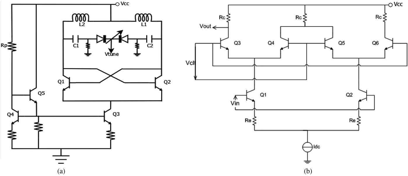
D) The BIST LC-voltage controlled oscillator
The BIST oscillator was designed with an LC cross-coupled VCO architecture (Fig. 3(a)), for several reasons: firstly, the oscillation frequency of this type of oscillator is less dependent on the process variations compared to other oscillator structures such as ring oscillator; secondly, passive elements of the resonator, i.e. inductors and capacitors, have small dimensions at 20 GHz. Furthermore, LC oscillators present a better phase noise than ring oscillators [Reference Abidi7].
Fig. 3. (a) The BIST LC-VCO circuit and (b) the BIST variable attenuator circuit.
This oscillator is modeled by two blocks: a resonator whose losses are modeled by a positive resistor R p and an active circuit, which is modeled by a negative resistor R n. A ratio of 6 was obtained between R p and R n. The oscillation frequency is controlled with a variable capacitor using two PN diodes connected in reverse parallel and biased by the control voltage V tune (Fig. 3(a)). At lower frequencies, the quality factor of the resonator, given by equation (1), is essentially limited by the inductance. At higher frequencies, it depends on the quality factor of both the inductance and capacitors. Based on the literature [Reference Verdier, Pérez and Gontrand8, Reference Zhan, Duster and Kornegay9], the quality factor of the tank circuit was chosen to be roughly equal to 10. Consequently, the inductance and the capacitor are equal to 250 pH and 253 fF, respectively.
 $$Q = \displaystyle{{R_p } \over {2\pi f_0\, L}} = 2\pi f_0 CR_p\comma \;$$
F) The BIST variable attenuator
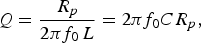
Two main topologies of variable attenuators can be considered: resistive attenuator and variable gain amplifier (VGA). As the bandwidth of a resistive attenuator is limited by the parasitic capacitance for small and accurate attenuation steps, the VGA architecture was chosen. The fully differential divider circuit (Fig. 3(b)) is selected because of a wider dynamic range than the single ended structures and a wider gain control range than the Gilbert cell [Reference Sansen and Meyer10].
The lower differential pair of the VGA is driven by the input signal. The control signal is applied to the bases of the upper differential pairs and drives their collector currents.
The AC voltage gain of the VGA for differential input and single ended output is given by:
 $$A_v = \displaystyle{{R_c } \over {2R_e }}\displaystyle{1 \over {1 + \exp \lpar {{V_{clt} } / {V_t \rpar }}}}.$$
In order to complete the design of the BIST generator, second harmonic rejection and phase noise have been simulated after parasitic extractions. They are better than 19 dBc at the maximum power and −93 dBc/Hz @1 MHz offset, respectively, which is comparable to previous studies [Reference Verdier, Pérez and Gontrand8, Reference Zhan, Duster and Kornegay9].
G) Electromagnetic coupling phenomena
The placement of the BIST circuit on the chip next to the DUT has been chosen to have the shortest external connection between the two circuits (Fig. 4(a)). The area of the BIST generator is about 30% of the DUT's area. However, the circuit is intended to be used in a complete receiver including the digital part. Hence, the surface of the BIST circuit will be very negligible compared to the final total die size.
Fig. 4. (a) Layout topology of the DUT including the BIST circuit and (b) representation of a point (M) in the plane (x, y) such that d >> the coil's radius R.
In order to limit the risk of coupling between the VCO inductor and the inductors of the DUT, an eight-shaped inductor placed perpendicularly to the other inductors is used for the BIST tank circuit. For a traditional octagonal coil, the intensity of the magnetic field evolves by (1/d 3), equation (3). However, for an eight-shaped inductor, it evolves by (1/d 4), equation (4), and it vanishes when d 1 = d 2 (Fig. 4(b)). Accordingly, compared to a traditional inductor, the reduction of the magnetic coupling using this type of coil can reach 20–30 dB, depending mainly on the distance and on the orientation of the coil [Reference Tesson and Wane11, Reference Poon12]. Parasitic extraction has been performed and simulation results clearly corroborate these theoretical assumptions.
 $$B\lpar d\rpar = \displaystyle{{\mu _0 .S.I} \over {4\pi }}\displaystyle{1 \over {d^3 }}\semicolon \;$$
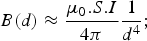 $$B\lpar d\rpar \approx \displaystyle{{\mu _0 .S.I} \over {4\pi }}\displaystyle{1 \over {d^4 }}\semicolon \;$$
III. MEASUREMENT RESULTS AND DISCUSSION
On-wafer probe testing was used to characterize the circuit. The BIST generator is supplied with 3.3 V and consumes 10 mA. It presents a frequency range between 17.5 and 23 GHz, and a dynamic power range between −41 and −24 dBm, as shown respectively in Figs 5(a) and 5(b). Measurement results correlate well with simulation results including parasitic elements. To evaluate the accuracy of the RF signal, statistical simulations were carried out. Monte Carlo simulations show that the frequency varies by ±1.4% (<±2.5% requirements) and the power by ±1.5 dB. So, when taking into account dispersions of manufacturing, the precision of the absolute gain measurement is about ±1.5 dB, whereas the DUT's gain specification is ±2.5 dB. The first measurements run have been performed on 12 circuits across the wafer. Measurements show that the frequency varies only by ±0.25% from a circuit to another. Concerning the power delivered by the generator, an accuracy better than 1 dB was measured for all attenuation steps. These results are very promising and need to be confirmed with a larger number of circuits.
Fig. 5. (a) The BIST oscillation frequency versus the control voltage of the BIST oscillator and (b) the BIST power versus the control voltage of the BIST attenuator.
The gain, the CP1 (Fig 6(a)), and the input reflection coefficient S 11 (Fig 6(b)) of the DUT were measured for the two states, ON/OFF, of the BIST circuit. The measurement results show that the BIST does not degrade RF performances of the receiver.
Fig. 6. (a) Measured gain, CP1 at 21.6 GHz and (b) measured input reflection coefficient of the DUT for the BIST circuit ON/OFF.
To evaluate the quality of the loopback technique, the DUT's gain (~16 dB) and CP1 (~ −30 dBm) were also measured using an external generator and then compared with the BIST generator in a loopback configuration. Figure 7 shows a good correlation between the two measurement techniques. The external loopback losses were characterized (~3 dB) and were taken into account in order to estimate the available power at the input of the DUT. The difference between the frequency of the signal from the generator at the input of the DUT and the oscillation frequency is negligible. This demonstrates a good isolation given by the succession of the buffer and of the attenuator for the BIST oscillator.
Fig. 7. Measurement of the receiver's gain with the loopback technique.
IV. CONCLUSION
The design of an embedded microwave generator for BIST applications is presented in this paper. The purpose of this BIST circuit designed in the SIGe:C BICMOS technology was to test, at low cost, the gain and the CP1 of a K-band satellite receiver chain. The measurements correlate well with the simulation results, including parasitic elements. The BIST generator dissipates 10 mA. It operates in a frequency range between (17.5 and 23 GHz) with an accuracy of ±0.25% and a power dynamic range of 17 dB with an accuracy better than 1 dB. Evaluation of extensive statistical data and extension to other RF parameter measurements will be performed in our future work. This BIST concept provides new perspectives in terms of production test strategy, cost reduction, and measurement accuracy for microwave and mm-wave ICs.
ACKNOWLEDGEMENTS
This work was supported by the EU project RF2THz. We thank Dr. Patrick Jean, Dr. Pascal Philippe, and Dr. Sidina Wane of NXP Semiconductors for helpful technical discussions and Dominique Lesenechal of LaMIPS for his support in the measurements.
Imene Lahbib received her Engineer diploma and M. Sc. degree in electronics in 2010 from the Ecole Nationale Supérieure d'Ingénieurs de Caen (ENSICaen) and the University of Caen, France, respectively. She is actually a Ph.D. student at NXP Semiconductors and the Laboratory of Microelectronics and Physics of Semiconductors (LaMIPS), Caen, France. Her main research interests include the RF BIST.
Mohamed-Aziz Doukkali received his Ph.D. in electronics in 1990 from the University of Montpellier (USTL). He started with CRISMAT Laboratory until 2000 to develop superconducting materials for microelectronics. From 2000 to 2008, he worked in failure analysis field in LaMIPS Laboratory. Since 2008 he has been working in the LaMIPS on BIST activities.
Philippe Descamps received his Ph.D. degree from the University of Lille, France, in 1992. In 1999, he became a full Professor at ENSICaen, France, where he currently heads the mixed research Laboratory LaMIPS. He is mainly involved in high-frequency characterization, modeling of microwave components and of the design of ICs for telecommunication applications. Pr Descamps is the author and co-author of more than 100 publications and conference papers.
Patrice Gamand received his Ph.D. in electronics in 1984 from the University of Lille. He started with Philips Research in France until 1993 to work on microwave sub-systems. He then moved to Philips Semiconductors to take over several positions in R&D for disk drive and telecommunication applications. In 2004, he was appointed general manager of the RF Innovation Center of Philips Semiconductors and then of NXP. In 2013, he was elected vice-president of IEEE MTT France chapter. Dr. Gamand is the author and co-author of more than 50 publications and conference papers and holds more than 32 patents.
Christophe Kelma is an RF test engineer at NXP Semiconductors (formerly Philips Semiconductors). His research interests include RF DFT, BIST, and radio communication ICs. He has a Diploma in engineering from ENSICaen, France.
Olivier Tesson received his Ph.D. from the University of Nantes in 2000. In 2001, he joined NXP Semiconductors (formally Philips Semiconductors) in France as CAD engineer. Since 2005, he has been a device modeling engineer in the RF Small Signal Department. He is currently Principal engineer, expert in passive integration and modeling of passive devices for RF and mm-wave applications holding more than 20 publications and 14 patents.