


I. INTRODUCTION
Ultra-wide band (UWB) technology has gained a lot of popularity among the researchers and wireless industries in the last few decades due to its attractive characteristics like low cost, low complexity, low spectral power density, high data resolution, very low interference, and extremely high data transmission rates [1]. Since then, UWB technology is expected to revolutionize prevalent communication systems. Furthermore, the emerging UWB wireless device trends demand embedded internal antennas that are compact in size and are lightweight in the limited space available without seriously sacrificing antenna performance. However, designing of such UWB antenna is not an easy task, several types of UWB antenna have emerged with its rapid growth [Reference Shameena, Mridula, Pradeep, Jacob, Lindo and Mohanan2–Reference Shrivastava, Gautam and Kanaujia6], among which slot antennas are the most promising candidate for UWB applications [Reference Ahmed and Sebak7–Reference Shirzad, Shokri, Amiri, Asiaban and Virdee12]. Generally, the microstrip-line-fed slot antenna does not add weight and size to the system rather it is suitable for portable applications. A microstrip-fed rectangular tuning stub with a tapered-shaped slot [Reference Azim, Islam and Misran13] and a square slot antenna with a pair of inverted-L grounded strips [Reference Sze and Chang8] have been reported for UWB applications. A T-shaped open-ended slot in the ground plane [Reference Sim, Chung and Lee10] and an antipodal tapered slot antenna with elliptically shaped strip [Reference Siddiqui, Antar, Freundorfer, Smith, Morin and Thayaparan11] are also presented to enhance the impedance bandwidth. A square ground-plane with two identical inverted-L shaped ground strips at two opposite corners of the slot antenna with an annular patch [Reference Shirzad, Shokri, Amiri, Asiaban and Virdee12] is used to attain UWB system. In [Reference Kim and Yun14], a C-shaped radiator and an inverted-L-shaped coupled strip extending from the ground plane is employed to fulfill the Federal Communications Commission (FCC) expectation. To enhance the bandwidth, a rectangular notch is etched vertically from the printed radiator and a strip is asymmetrically attached to the radiator [Reference Chen, See and Qing15]. A wide-band rhombus-like wide-slot antenna with an offset microstrip-fed line [Reference Jan and Kao16] and printed microstrip-line-fed rhombus slot antenna with a pair of parasitic strips [Reference Jan and Wang17] is proposed for wide band applications. In [Reference Lin, Yu and Huang18], a coplanar waveguide-fed rhombus slot antenna is proposed for dual-band operation. In above discussed papers, the rhombus slot is used either for wide band or dual band. In the present endeavor, the rhombus-shaped slot antenna is being proposed for ultra wide applications. The advantages of wide rhombus-shaped slot radiator is that it has greater bandwidth and comparatively less stringent tolerances on the mass alignment for printing as compared with the other type of narrow slot radiator. The comparison of the proposed antenna with various antennas is listed in Table 1. It is evident from the comparison that the proposed antenna has smaller size and offers larger bandwidth than all reported antennas.
Table 1. Comparison of various antennas for UWB applications.

In this paper, a novel rhombus-shaped slot antenna is presented for UWB applications as illustrated in Fig. 1. The antenna is designed on 1.6 mm thick FR4 epoxy dielectric substrate (relative permittivity of 4.4) with an overall size of 19 × 21 mm2. The proposed design is very simple and compact to other reported antennas for UWB application. A good 10 dB impedance matching is achieved by adequately adjusting the parameters of the rhombus-shaped slot and feed-line. The design considerations for obtaining UWB characteristics are considered, and the simulation and experimental results are presented. A fair agreement with simulated results, the measured impedance bandwidth of the proposed antenna is 10.14 GHz from 2.78 to 12.92 GHz (defined by 10 dB return loss). The details of entire design are presented in the following sections:

Fig. 1. Schematic configuration of the proposed compact rhombus-shaped slot antenna.
II. ANTENNA DESIGN
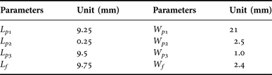
The slot antenna radiates radio frequency energy through slots or along a conducting surface; therefore, selection of appropriate slot shape becomes very important. Conventionally, the slot antenna consists of a radiator formed by cutting slots on large metal surface and fed by microstrip-lines. Thus, in the proposed design, a slot is cut from a 45° rotated rectangle to form a rhombus-shape and excited by a microstrip-line. The rhombus-shaped slot has an overall length of L p1 + L p3 and width of W p1. The length and width of the rectangle that is attached to the rhombus-shaped is L p2 and W p2, and the width of the rhombic arm is W p3. A microstrip-line of length L f and width W f is placed on opposite side of the radiator to improve the impedance bandwidth, radiation performance, and to reduce the effect of ground plane. The slot and feed-line parameters are optimized to achieve a miniaturized design and optimized dimensions as listed in Table 2.
Table 2. Design parameters of the proposed rhombus-shaped slot antenna.
The predicted current distributions at different frequencies are shown in Fig. 2. The simulated surface current distribution in Fig. 2(a) shows that the current is distributed over entire rhombus-shaped slot and more prevalent at the edges of the rhombus-shaped slot and the feeding line. Thus, it is found that the lower arms and half of upper arms of the rhombus-shaped slot radiator generate the resonant mode of 3.3 GHz. For the resonance around 6.35 GHz in Fig. 2(b), the current is distributed mainly over the edges of rhombus-shaped slot and feed-line. It is seen that the concentration of simulated current on lower arms and half portion of upper arms of the rhombus-shaped slot is less as compared with Fig. 2(a). The result in Fig. 2(c) reveals that surface current of the higher resonant mode (11.42 GHz) is mainly distributed on the lower arms of the rhombus-shaped slot. Thus, it is found that the lower arms also contribute in the generation of higher modes of the UWB band. From the above discussion, it is evidently clear that the proposed rhombus-shaped slot antenna will work as a UWB antenna.

Fig. 2. Simulated surface current distribution at the various sampling frequencies of the proposed rhombus-shaped slot antenna.
The various steps of the slot antenna design are illustrated in Fig. 3. Initially an inverted triangular structure is used to achieve the ultra- wide bandwidth but this structure excites only higher resonating modes as shown in Fig. 3. However, as a triangular slot is cut inside this triangle-shape, an overall impedance of the antenna get change, consequently, it excites two resonant modes one at higher frequency due to triangular shape and lower mode is excited due to triangular slot. Furthermore, when the structure is modified to the rhombus-shaped slot it excites three resonant modes; two modes are excited as per earlier explanation and middle resonant mode is excited due to extension of triangular slot into rhombus-shaped slot. As all three resonant modes are overlapped, the proposed design will exhibit a UWB performance.

Fig. 3. Simulated return loss against frequency for the antenna with inverted triangular, inverted triangular slot, and the rhombus-shaped slot.
III. PARAMETRIC STUDY OF THE PROPOSED ANTENNA
In this section, the influence of the different design parameters on antenna performance is presented and discussed. At a time one parameter is studied, the others are kept constant. The results of these parametric studies provide a useful strategy to optimize the design before final fabrication. Ansoft high frequency structure stimulator [19] simulator based on the finite element method is used to perform the parametric study of the design.
A) Variation of the rhombus-shaped slot parameters
Figure 4 depicts the effect of the length L p3 of the upper arms of the rhombus-shaped slots on the simulated return loss of the proposed antenna. It is evident from Fig. 4 that the overall impedance of the antenna is changed as the value of L p3 increases from 3.5 to 9.5 mm. This change in impedance mainly influence the impedance mismatch at the lower and middle bands (from 3 to 6 GHz) as this part of rhombus-shaped slot is responsible for middle band. Therefore, the optimized value of L p3 is chosen 9.5 mm. The effect of width W p1 of the rhombus-shaped slot on the simulated performance of antenna is shown in Fig. 5. It is keenly observed that the impedance mismatch at the entire UWB band improves greatly as the width is varied from 13 to 21 mm. Therefore, it is decided on W p1 = 21 mm as the optimum value with the bandwidth from 2.78 to 12.92 GHz, covering the entire UWB band.

Fig. 4. Simulated return loss against frequency for the microstrip-fed compact rhombus-shaped slot antenna with various length L p3.

Fig. 5. Simulated return loss against frequency for the microstrip-fed compact rhombus-shaped slot antenna with various width W p1.
Figure 6 shows the influence of the arm width W p3 of the rhombus-shaped slot over the antenna performance. It is observed that as the width of the antenna varies from 0.5 to 1 mm the bandwidth of the antenna increases greatly and decreases furthermore because the slot contributes a lot in energy radiation. Thus, the optimum value of W p3 is chosen 1 mm to cover entire UWB band.

Fig. 6. Simulated return loss against frequency for the microstrip-fed compact rhombus-shaped slot antenna with various width W p3.
The effect of the length L p2 of rectangular strip attached to bottom of the rhombus-shaped slot on the return loss of the antenna from 0.25 to 6.75 mm is depicted in Fig. 7. It is found that the bandwidth of the antenna greatly decreases as the value of L p2 increases from 0.25 to 6.75 mm. Therefore, it is decided that the optimum value of L p2 = 0.25 mm.

Fig. 7. Simulated return loss against frequency for the microstrip-fed compact rhombus-shaped slot antenna with various length L p2.
B) Variation of microstrip feed-line parameters
Figure 8 illustrates the effect of feed length L f on the performance of the antenna. The change in the feed length L f from 6.75 to 9.75 mm mainly improves the impedance matching of the antenna with a slight shift in the entire band towards lower frequency band and decreases the impedance matching furthermore. Therefore, it is decided on L f = 09.75 mm as the optimum value with the bandwidth from 2.78 to 12.92 GHz, covering the entire UWB band.

Fig. 8. Simulated return loss against frequency for the microstrip-fed compact rhombus-shaped slot antenna with various length L f .
As illustrated in Fig. 9, the bandwidth of the antenna slightly shifts towards the higher frequency with the feed width W f of the antenna, from 0.6 to 3 mm. However, the mismatch at the frequency from 6 to 10 GHz of the UWB band improves with the feed width. Therefore, it is decided on W f = 2.4 mm as the optimum value for the bandwidth from 2.78 to 12.92 GHz, covering the entire UWB band.

Fig. 9. Simulated return loss against frequency for the microstrip-fed compact rhombus-shaped slot antenna with various length W f .
IV. TIME DOMAIN ANALYSIS
Time domain analysis of the proposed UWB antenna is also carried out to measure the pulse handling capability and fidelity factors. These studies are carried out by placing two antennas (transmitter and receiver) in the far-field region (face-to-face, side-by-side y-direction, and side-by-side x-direction). The transmitter is excited by a Gaussian signal that complies with the FCC indoor and outdoor power spectrum mask. Fig. 10 shows the input and received signals in the far-field region (side-by-side y-direction, side-by-side x-direction, and face-to-face).

Fig. 10. Input and received pulse in different orientations of proposed antenna.
The low-distortion time domain performance of the miniaturized antenna is also confirmed by calculating the fidelity factor. Fidelity factor is used to measure the degree of similarity or correlation between the transmitted and received pulses. Fidelity factor can be calculated using following equation,
 $$F = \max \left \vert {\displaystyle{{\int_{ - \infty} ^\infty s_t (t)s_r (t + \tau )dt} \over {\sqrt {\left( {\int_{ - \infty} ^\infty s_t (t)^2 dt} \right)\left( {\int_{ - \infty} ^\infty s_r (t)^2 dt} \right)}}}} \right \vert,$$
where s t (t) and s r (t) are input and received signals. The fidelity factors in the case of face-to-face, side-by-side y-direction, and side-by-side x-direction are obtained as 75, 79, and 78%, respectively.
V. RESULTS AND DISCUSSION
To verify the design, the antenna parameters such as impedance bandwidth and return-loss are measured using Agilent N5230A vector network analyzer. The measured and simulated return-loss results of the proposed antenna are shown in Fig. 11. From the measured results, it is found that the antenna offers an ultra-wide bandwidth of 10.14 GHz (from 2.78 to 12.92 GHz) with good accord to the simulated results. It is evidently clear that the designed antenna covers entire UWB band.

Fig. 11. Measured and simulated return loss against frequency for the microstrip-fed compact rhombus-shaped slot antenna.
Figure 12 shows the gain and efficiency of the proposed antenna. It is observed that the gain of the proposed antenna varies from 0.84 to 1.76 dB over the entire operating band. The proposed antenna shows a low gain due to small size and wide rhombus-shaped slot radiator. Figure 12 shows that the efficiency of the proposed antenna varies from 84 to 95% over the entire operating band. The efficiency of the antenna is excellent as ohmic resistance of the proposed antenna is less.

Fig. 12. Gain and efficiency against frequency for the proposed antenna.
The two-dimensional far-field radiation patterns containing co-polar and cross-polar in the E-plane (xz-plane) and H-plane (yz-plane) at sampling frequencies of 3.3, 6.35, and 11.42 GHz, respectively, are plotted in Fig. 13(a)–(c). It is found that the antenna has nearly good omni-directional radiation patterns at all sampling frequencies in the E- and H-plane. This pattern is suitable for applications in most wireless communication equipment, as expected.

Fig. 13. Radiation patterns of the proposed compact rhombus-shaped slot antenna at (a) 3.3 GHz, (b) 6.35 GHz, and (c) 11.42 GHz sampling frequencies. Measured results – and simulated results – .
VI. CONCLUSION
A novel microstrip-line-fed rhombus-shaped slot antenna for UWB antenna is successfully demonstrated and implemented. The prototype with an overall size of 19 × 21 × 1.6 mm3 is fabricated and tested. The measured results validate the design and the impedance bandwidth can operate from 2.78 to 12.92 GHz (10.14 GHz), which evidently covers entire UWB (3.1–10.6 GHz).
 Richa Chandel was born in Dehradun, India, in 1986. She completed her B. Tech. in Electronics and Communication Engineering from Uttar Pradesh Technical University, Lucknow, India and M. Tech (Digital Signal Processing) from Uttarakhand Technical University, Dehradun, India in year 2010 and 2013, respectively. Presently, she is working towards her doctorate degree from G B Pant Engineering College, Pauri Garhwal (INDIA). She has published many research papers in peer reviewed journals/conferences. Her main research interest is designing and modeling of ultra-wideband microstrip antenna.
 Anil Kumar Gautam was born in Noida, Uttar Pradesh, India. He received his B.E. degree in Electronics and Communication Engineering from Kumaon Engineering College, Almora, India and his Ph.D. degree in Electronic Engineering from Indian Institute of Technology, Banaras Hindu University, Varanasi, India, in 1999 and 2007, respectively. He joined the Department of Electronics and Communication Engineering, G B Pant Engineering College, Pauri Garhwal, India, in 2000, as an Assistant Professor and he has been an Associate Professor there since 2009.
Dr. Gautam is an active member of Board of Study (BOS), Academic council, and many other academic committees of G B Pant Engineering College (GBPEC), Pauri. He is also a member of BOS of HNB Garhwal Central University, India and Uttarakhand Technical University, Dehradun, India. He is nominated as Nodal Officer, TSP, and SCSP Grants by Government of Uttarakhand and executed several projects under these grants. He has supervised 15 M. Tech. and one Ph.D. thesis and presently supervising nine Ph.D. thesis in the area of microstrip antenna.
Dr. Gautam is the author/co-author of more than 70 research papers published in the refereed international journals and conferences such as IEEE, Microwave and Optical Technology Letters, Springer, etc. He is the author of 13 books in the field of Electronics Engineering, Digital Electronics, Antenna and Microwave Engineering. He is a member of IEEE (USA) and many other technical societies. He is also in reviewers panel of IEEE, Transaction on Antenna and Propagation, IEEE, Antenna and Wave Propagation Letters, IET Microwaves, Antennas & Propagation, Personal and wireless communication, Springer, International Journal of Electronics, International Journal of Microwave and Wireless Technologies, International Journal of Antenna and Propagation, etc. His main research interests are in design and modeling of active microstrip antenna, microstrip antennas with defected ground structure, ultra-wide bandwidth antennas, and reconfigurable antennas, reconfiguration antenna array, circular-polarized antenna, etc.
 Binod Kumar Kanaujia is presently working as an Associate Professor in the Department of Electronics and Communication Engineering in Ambedkar Institute of Advanced Communication Technologies and Research (formerly Ambedkar Institute of Technology), Geeta Colony, Delhi. Dr. Kanaujia joined this Institute as an Assistant Professor in 2008 through selection by Union Public Service Commission, New Delhi, India and served on various key portfolios i.e. Head of Department, In-charge Central Library, Head of Office, etc. Before joining this institute he served in the M.J.P. Rohilkhand University, Bareilly, India as a Reader in the Department of Electronics and Communication Engineering and also as Head of the Department. He has been an active member of Academic Council and Executive Council of the M.J.P. Rohilkhand University and played a vital role in academic reforms. Prior, to his career in academics, he worked as an Executive Engineer in the R&D division of M/s UPTRON India Ltd.
Dr. Kanaujia completed his B. Tech. in Electronics Engineering from KNIT Sultanpur, India in 1994. He did his M. Tech. and Ph.D. in 1998 and 2004, respectively, from the Department of Electronics Engineering, Indian Institute of Technology Banaras Hindu University, Varanasi, India. He has been awarded Junior Research Fellowship by UGC Delhi in the year 2001–2002 for his outstanding work in electronics field. He has keen research interest in design and modeling of microstrip antenna, dielectric resonator antenna, left-handed metamaterial microstrip antenna, shorted microstrip antenna, ultra-wideband antennas, and reconfigurable and circular-polarized antenna for wireless communication.
He has been credited to publish more than 105 research papers with more than 200 citations with h-index of 10 in peer-reviewed journals and conferences. He has supervised 45 M. Tech. and three Ph.D. research scholars in the field of microwave engineering. He is a reviewer of several journals of international repute i.e. IET Microwaves, Antennas and Propagation, IEEE Antennas and Wireless Propagation Letters, Wireless Personal Communications, Journal of Electromagnetic Wave and Application, Indian Journal of Radio and Space Physics, IETE Technical Review, International Journal of Electronics, International Journal of Engineering Science, IEEE Transactions on Antennas and Propagation, AEU-International Journal of Electronics and Communication, International Journal of Microwave and Wireless Technologies, etc. He has successfully executed four research projects sponsored by several agencies of Government of India, i.e. DRDO, DST, AICTE, and ISRO. He is also a member of several academic and professional bodies, i.e. IEEE, Institution of Engineers (India), Indian Society for Technical Education and the Institute of Electronics and Telecommunication Engineers of India.


