1. INTRODUCTION
The magnetically insulated diode (MID) with the radial B-field and an induction plasma source on the anode is the most advanced tool, which is successfully used to generate high-power intense ion beams (HIIB), different gases and nano- and sub-microsecond pulses (Greenly et al., Reference Greenly, Ueda, Rondeau and Hammer1988; Lamppa et al., Reference Lamppa, Stinnett, Greenly, Renk and Crawford1995; Bystritskii et al., Reference Bystritskii, Garate, Rostoker, Song, VanDrie, Anderson, Qerushi, Dettrick, Binderbauer, Walters, Matvienko, Petrov, Shlapakovsky, Polkovnikova and Isakov2004; Renk et al., Reference Renk, Provencio, Prasad, Shlapakovski, Petrov, Yatsui, Jiang and Suematsu2004).
The important task in developing MID with active plasma sources is providing the required structure of the magnetic field in the acceleration gap, which has a determining impact on the dynamics of the electron and ion components in the diode current. One of the main requirements to the diode structure is the correspondence of the distribution of the magnetic field in the diode to the topology of В = f(1/r), which is evident from the magnetic flux constancy ψ = const. in the acceleration gap. As a result, the magnetic surfaces in the acceleration gap must be parallel to each other and to the electrode. The latter can be easily reached by using the anode which is non-transparent for the pulsed magnetic field. The other important requirement is the conservation of B-flow in the acceleration gap during a pulse; its quick redistribution is related to the emergence of a closed Hall electron current and also requires the usage of the anode which is non-transparent for a magnetic field. This requirement is extremely important to control MID impedance and to maintain the efficiency of HIIB generation, especially for microsecond pulses. When the power is transferred to loading, the behavior of impedance is determining and is intensively studied for high-current ion and electron diodes (Cai et al., Reference Cai, Liu, Ju, Zhao and Qiu2014; Hayashi et al., Reference Hayashi, Ito, Tamura, Kudo, Takaura, Kashine, Takahashi, Sasaki, Kikuchi, Harada, Jiang and Tokuchi2015).
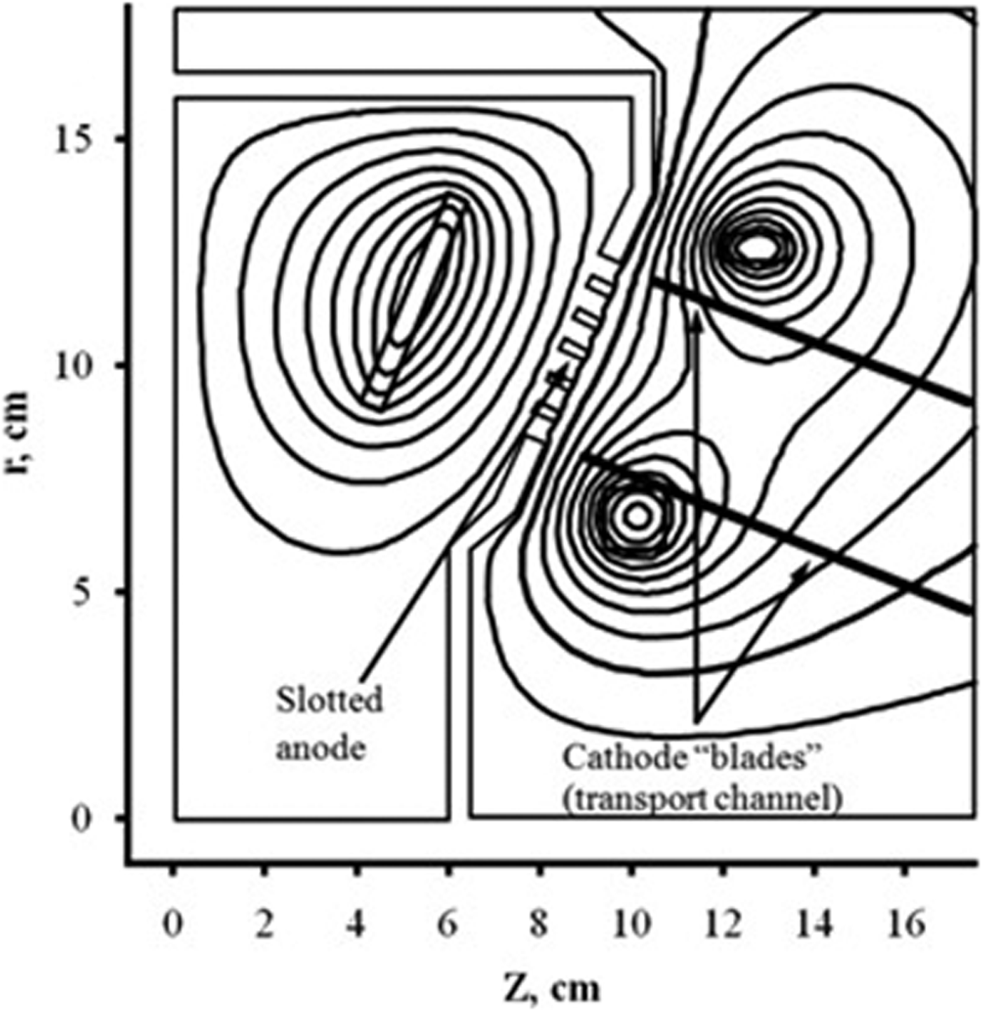
In the given paper, we investigate a diode configuration (Bystritskii et al., Reference Bystritskii, Garate, Rostoker, Song, VanDrie, Anderson, Qerushi, Dettrick, Binderbauer, Walters, Matvienko, Petrov, Shlapakovsky, Polkovnikova and Isakov2004) with a grid-like anode with azimuthal-symmetrical slots to puff plasma into the acceleration gap, which is located across an annular gap between the cathodes (Fig. 1). The presence of the azimuthal slots in the anode causes the deflection of the shape of the magnetic surface from the geometry of the anode surface. Due to the B-field deflection to the anode slots, the magnetic surface forms regular waves (ripple) in the radial direction. Thus, there arises the task of an acceptable magnetic field distortion in the region of the anode and reservation of the requirements to the B-field topology regarding the compensating action of the shock induction coil. The other most important issue is the elimination of the magnetic surface distortion in the cathode region (edge effects). The configuration of the cathode surface is effected by the parameters, which are difficult to be accounted using calculation. As the analysis shows, these effects are mainly associated with the accuracy of the configuration of the diode magnetic field coils and the shape of the anode surface across their location. In this situation, the optimization of the B-field topology in the acceleration gap by comparing the measured and calculated values of the magnetic field strength becomes important.

Fig. 1. The topology of the magnetic field of the B-diode with an induction plasma source. The induction coil is on the left; the cathode coils of the magnetic field of the diode are on the right.
The objective of the paper is the calculation and optimization of the B-diode magnetic field structure with induction plasma source for further estimation of the quality of the topology of the magnetic field in the diode gap based on the HIIB characteristics.
In Section 2, the calculation model is briefly described. In Section 3, the results of the B-field topology calculations are given, the B-field is created by the shock induction coil and the coils of the magnetic system of the diode for the case of the solid diode. In Section 4, the calculation results of the B-field structure are detailed in the domain of the anode slot. The results of the optimization of the magnetic field structure in the acceleration gap are presented in Section 5. In conclusion, in Section 6, the results are summarized.
2. CALCULATION MODEL
The schematic of MID is shown in Figure 1. The coils of the diode magnetic system and a shock induction coil are located inside the chamber with perfectly conducting walls and therefore the applied boundary conditions are ψ = 0.
We solve the task using a discrete grid inside the chamber. The coil current I θ may be then represented as a current density J θ defined on the gridpoints. Due to a cylindrical symmetry, the magnetic field can be obtained from the Ampere's law for an azimuthal current density and given as:
 $$\nabla \times B = \displaystyle{{4{\rm \pi}} \over c}J_{\rm \theta}. $$
In a cylindrically symmetric system with an azimuthal current, the vector potential A has only an azimuthal component, which may be represented by a scalar flux function ψ(r, z) = rA θ. The Ampere's law is then:
 $$\displaystyle{{\partial ^2 {\rm \psi}} \over {\partial r^2}} - \displaystyle{1 \over r}\displaystyle{{\partial {\rm \psi}} \over {\partial r}} + \displaystyle{{\partial ^2 {\rm \psi}} \over {\partial z^2}} = - \displaystyle{{4{\rm \pi} r} \over c}J_{\rm \theta}. $$
This is the Grad–Shafranov equation. Once it has been solved using suitable boundary conditions, the magnetic field can be obtained from:
 $$B_r (r,z) = - \displaystyle{1 \over r}\displaystyle{{\partial {\rm \psi} (r,z)} \over {\partial z}}\quad {\rm and}\quad B_z (r,z) = \displaystyle{1 \over r}\displaystyle{{\partial {\rm \psi} (r,z)} \over {\partial r}}.$$
Equation (2) is an elliptic equation which can be solved using standard methods. Firstly, in Section 3 below, we use a finite-difference method (the Alternating Direction Implicit method) on a rectangular grid neglecting the slots in the anode. The result is used to obtain the boundary conditions for a more limited domain which is centered near the anode slots. In Section 4, we use a finite element method (using the ELLIPT2D Python software package) on an irregular triangular grid to find the magnetic field in the region of the anode slots.
3. TOPOLOGY OF B-FIELD FOR A SOLID ANODE
In the given section, we calculate B-field strengths without taking into account the influence of perturbation of the slots on the anode. The results will be used to obtain the boundary conditions when calculating the magnetic field in the region of the anode slots. The cross-section of the r − z diode is shown in Figure 1. The conical shock coil is located inside the conducting anode with close-lying walls. We assume that the shock coil with internal and external radiuses r sc1 = 96 and r sc2 = 130 mm, respectively, is wound in such a way that only azimuthal current component is significant. The internal and external coils of the magnetic system of the diode have 7 and 12 turns, respectively, with 10 kA current per turn. The coils are located in the cathode screens with internal and external radiuses r c1 = 80 and r c2 = 120 mm. In this case, the coils of the magnetic system of the diode do not have closely located boundaries with perfect conductors, as in the case with a shock coil except for the screen which is transparent for the magnetic field. As a result, the boundary conditions ψ = 0 for an ideal conductor are specified on the walls of one chamber. In Figure 1, the rightmost and uppermost boundaries on the domain were set at z = 50 and r = 40 cm, respectively. The left boundary is still a conical surface of the anode. The results of the calculation of the topology of the magnetic field for a solid anode and current in a shock coil of I θ = 22.3 kA are shown in Figure 1.
4. FIELD CLOSE TO THE ANODE SLOTS
To solve Eq. (2), in and around the slots, we used the ELLIPT2D finite element software package, which is well adapted for handling domains with holes in them. A limitation on this package is that it is only effective, if there are <10 000 vertices in the triangular grid. Therefore, to obtain the accurate results around the slots, it is necessary to solve the equation on a reduced domain. We note from Figure 1 that at a medium radius of the anode, at a distance of 1.5 cm from its surface, the field lines are almost parallel to the anode. We therefore construct a reduced domain, shown in Figure 2, which extends 1.5 cm on either side of the anode and centers on a single slot. Our observation that the field lines are approximately parallel to the conical anode allows us to specify simplified boundary conditions on this reduced domain. Along the left and right boundaries, we specify the Dirichlet boundary conditions, using two constant values of ψ, which are obtained from the calculations in Section 3. Along the upper and lower boundaries we used the Neumann boundary conditions. The white rectangles in the domain represent the 2.5 mm brass separations between the 5-mm slots in the 5-mm thick anode. The boundary condition on the white rectangles is ψ = 0.
Fig. 2. The topology of the magnetic field of the B-diode in the domain of the 5-mm wide anode slot. Curves represent the magnetic field line distribution and color represents magnetic field strength. Points A, B, C, D, E, and F are used to specify the B-field distribution and are referred to the next figure. The diode magnetic field coils are on the right side.
In this case, the Dirichlet boundary conditions were calculated using a total current in the shock coil of 25 and 8 kA per turn in the shock coil. The result in Figure 2 represents the field lines superimposed on a color scheme which represents the magnetic field strength. The points labeled A, B, C, D, E, and F are used in Figure 3, where the magnetic field strength is plotted along the straight lines AB, CD, and EF for anode slots with a width of 5 and 3.5 mm.
Fig. 3. Magnetic field strengths along the straight lines AB, CD, and EF from Figure 2. Curves 1 and 2 are the width of the anode slot of 5 and 3.5 mm, respectively.
The main results of the analysis of the obtained dependencies are as follows.
• The expected difference of the magnetic field strength in the points C and В are related to the reduction of the field with increasing the radius according to the function B = f(1/r).
• B-field distortions in the acceleration gap of the diode are located in the region of the anode with an extension, which does not exceed the half-width of the anode slot, and decrease with decreasing the slot dimensions. Thus, for the 5-mm slot the field strength at a given distance is ~80% from the undisturbed value on the anode, and for the 3.5-mm slot it is ~93%.
5. OPTIMIZATION OF THE MAGNETIC FIELD STRUCTURE IN THE ACCELERATION GAP
Figure 4 presents the calculated and measured distributions of the magnetic field on the conical surface of the anode of the diode with 8-mm acceleration gaps. The measurements were made using a gauge with a thickness of 1 mm and a size of 2 × 3 mm2. The measured values for a solid anode (curve 2 in Fig. 4) reveal the distortion of the magnetic surface in the edge regions of the internal and external cathodes with radiuses of r k1 = 80 and r k2 = 111 mm, respectively. These effects often appear in real constructions and depend on many factors, including the values of the acceleration gap that is equal to the distance between the center of gravity of the coils and the anode surface. The impact of the change of the anode profile in the region across the diode B-field coils (Fig. 4) is shown with curve 3 in Figure 4 for the anode with 5-mm slots. The resulting distribution of the B-field with an accuracy of ~15% caused by a deflection into anode slots coincides with the distribution of В = f(1/r) for the specified geometry of the diode.
Fig. 4. Magnetic field induction distribution on the surface of the anode: calculation of B = f(1/r) for a solid anode (1); measured values at a distance of 1 mm from the plate of the solid anode (initial shape) and with the slots of 5 mm (final shape), respectively (2, 3); the geometry of the initial (a) and final (b) shape of the anode; A-anode, K-cathode. r a1, r a2; r c1, r c2; r b1, and r b2 are internal and external radii of the emission surface on the anode, cathode, and break points on the anode.
6. CONCLUSION
We performed the calculation and the optimization of the structure of the radial insulating magnetic field in the acceleration gap of the high-power ion diode with an induction plasma source. The specifications of the task under examination are related to the azimuthal-symmetrical slots in the anode to pump plasma in the acceleration gap.
The obtained results reveal the appearance of the B-field perturbation as waves in the radial direction localized in the near-anode region. The amplitude of perturbation is a half-width of an anode slot and for the slots of 5 and 3.5 mm has the values of the magnetic field in these points of 80 and 93%, respectively. The geometric transparence of the anode is 75 and 50% for the specified dimensions of the anode slots. The compensating impact of the magnetic field of the shock induction coil on the perturbation of a magnetic field onto the anode surface in the acceleration gap for the anode slot of 3.5 mm becomes insignificant.
The change in the anode profile in the region across the diode magnetic system coils enables one to optimize the structure of the magnetic field by maintaining topology of В = f(1/r) in the near-anode region accurate to ~15% for the slots of 5 mm and the acceleration gap of 8 mm. The specified size of the anode slot can be considered as maximum possible and available that was also proved by insignificant differences of the research results of the electron magnetic insulation for a solid anode and with the corresponding anode slots. These results will be published later.
ACKNOWLEDGEMENT
The work is supported by the Russian Science Foundation, Grant No. 14-19-00439.