


I. INTRODUCTION
Recent researches in plasmonics areas have led to important progress in development of various metal–insulator–metal (MIM) plasmonic devices. Plasmonic studies have almost exclusively focused on pure metallic nanostructures and passive components with properties fixed by the nanostructure structural parameters. As the greatest challenge, real-life applications require active control of plasmonic signals in nano-optic devices [Reference Gu1, Reference Gao, Tang, Hu, Guo, Wang and Zhou2]. Moreover, it is advantageous to be able to tune plasmonic passive devices. All these can be realized if plasmonic nanostructures are hybridized with functional materials. Development of electro-optical materials and integrating them with plasmonic nanostructures, give rise to great research effort in proposing active plasmonic devices [Reference Kossyrev3]. Electro-optic control of plasmonic signals can be provided by the use of nematic LC (N-LC). N-LC, because of high levels of controllable birefringence, supports the external manipulation of plasmonic signals via external electric fields. Recently, LC thin films with a thickness of a few nanometers have attracted much interest due to their relaxation time of less than a nanosecond [Reference Weiss, Woll and Johannsmann4]. There has been concerted research to investigate the properties of thin LC layers both theoretically and experimentally [Reference Dorjgotov, Bhowmik and Bos5–Reference Werner, Kwon, Khoo, Kildishev and Shalaev7]. With its low driving voltage and low-cost fabrication technology, LC technology seems to be an outstanding candidate for tunable plasmonic devices and is proposed for various applications [Reference BahramiPanah, Mirtaheri and Abrishamian8–Reference Dridi and Vial10].
In order to design plasmonic devices, it is necessary to derive the dispersion relation of the desirable structure. Anisotropic behavior of the LC affects the propagation of surface plasmons polaritons (SPPs), and makes the inclusion of anisotropy in the theory inevitable. The existence of transverse magnetic (TM) modes at the interface of an anisotropic uniaxial dielectric and a metal has been discussed in [Reference Krokhin, Neogi and McNeil11, Reference Smolyaninov12]. However, these works have been restricted to materials with diagonal dielectric tensors, and the resulting equations are nearly identical to those used in the original isotropic media. A simplified theoretical study of electromagnetic wave propagation through insulator–metal–insulator and MIM structures consisting of anisotropic dielectric layers with off-diagonal dielectric tensor has performed [Reference Jacob, Babu, Mathew and Mathew13]. However, the principal axes of the anisotropic slab are simply chosen parallel to the metal/anisotropic interface and the directions of the electromagnetic fields are chosen in a manner which the electric field vector is in parallel with electric flux density. In a recent work, the guided optical modes of a planar plasmonic waveguide filled with a generic anisotropic medium have been studied [Reference Rukhlenko, Premaratne and Agrawal14].
However, previous works on the fundamental guided dispersion characteristics are still incomplete. In particular, discussions related to the electro-optic control of plasmonic signals are insufficient, which can be significant design guidelines for active plasmonic devices. Dispersion relation of LC dielectric-loaded MIM waveguides has not been extracted yet and there is not any deep analysis of this structure in the previous literatures. In this paper, we propose a hybrid plasmonic nanostructure consisting of nanostructured metals combined with LCs to enable active functionalities in plasmonic circuitry. The dispersion relations corresponding to both symmetric and antisymmetric modes in the metal–liquid crystal–metal (M–LC–M) structure are derived without any approximation and numerically solved. The motivation for considering LC is the possibility of utilizing the LC parameters in controlling the plasmonic signals. Our results have some potential application in designing tunable compact nanophotonic devices.
II. GENERAL DISPERSION RELATION OF M–LC–M STRUCTURE
The structure under study, shown in Fig. 1, comprises a slab of thickness 2a with its interfaces orthogonal to the x-axis, filled with N-LC and sandwiched between two silver layers. Dispersive behavior of silver is estimated using Drude model. This structure acts as a waveguide for the SPP propagating along the z-direction in the form of a waveguide mode for the TM-polarized case. To consider only excitation of the fundamental SPP mode, the width of the LC layer is chosen to be much smaller than the wavelength of incident light. In general anisotropic media, the properties of the medium are expressed in tensor form. In this paper, we assume that our structure is only electrically anisotropic. Assuming the optical axis of the anisotropic molecules in the X–Z-plane, the dielectric tensor of the LC medium is given by [Reference Dridi and Vial10]:
 $$\overline{\overline \varepsilon} = \left[ {\matrix{ {n_e^2 \,\,{{\cos} ^2}\theta + n_o^2 \,\,{{\sin} ^2}\theta n} & 0 & {\left( {n_e^2 - n_o^2} \right)\,\,\sin \theta \,\,\cos \theta} \cr 0 & {n_e^2} & 0 \cr {\left( {n_e^2 - n_o^2} \right)\,\,\sin \theta \,\,\cos \theta \,} & 0 & {n_o^2 \,\,{{\cos} ^2}\theta + n_e^2 \,\,{{\sin} ^2}\theta} \cr}} \right],$$
where n o and n e are the ordinary and extraordinary indices of refraction, respectively. In the equations above, θ, called tilt angle, is the angle between the optical axis of the anisotropic molecules and the z-direction. In the entire paper, n e and n o are considered to be 1.737 and 1.518, respectively, which belong to a positive N-LC (E7) at room temperature.

Fig. 1. General Schematic of the M–LC–M waveguide structure [Reference Bahramipanah, Abrishamian and Mirtaheri15].
The amount of voltage needed to switch an N-LC modulator is a function of the specific material used, cell thickness, and alignment. Our device takes advantage of the metallic nature of the structure, where the metal walls can serve as electrodes. A low-frequency voltage of varying value is applied at the upper silver layer; the electrical path terminates at the lower metal film, which is grounded. The electric field induces a reorientation of the LC molecules, which tend to align with the applied field, modifying the overall electrical and subsequently optical properties of the LC material. The exact profile of the molecular orientations and the extent of the LC-switching depend on the value of the applied voltage, the molecular anchoring conditions at the walls, the geometry of the structure, and the material properties of the LC and the surrounding isotropic materials. As the applied voltage increases, the tilt angle of each molecule increases because the LC molecules tend to align with the electric field. For a sufficiently high voltage, the strong electric field inside the waveguide plays a significant role in the LC-orientation behavior. Because of nanometer-sized waveguide, the electric field inside the waveguide is strong enough to switch all the nematic molecules; and the strong electric field dominates the anchoring condition at the M–LC interface. Thus, the LC is considered to be fully switched, when the nematic director of the material tends to align in parallel to the x-axis, so that the tilt angles of the molecules in this area all approximate 90°. Hence, good alignment quality and device switching can be achieved.
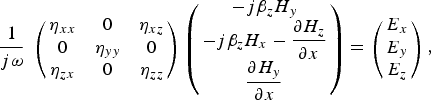
To obtain the dispersion relation, we first derive the wave equation inside the LC medium. Just the TM condition is considered. For propagation along the z-direction and homogeneity in the y-direction, propagation of the magnetic field in LC medium is described as follows:
 $$\displaystyle{1 \over {j\omega}} \; \overline{\overline \eta} \; \left( {\matrix{ { - j{\beta _z}{H_y}} \cr { - j{\beta _z}{H_x} - \displaystyle{{\partial {H_z}} \over {\partial x}}} \cr {\displaystyle{{\partial {H_y}} \over {\partial x}}} \cr}} \right) = \left( {\matrix{ {{E_x}} \cr {{E_y}} \cr {{E_z}} \cr}} \right),$$
 $$\displaystyle{1 \over {j\omega}} \; \left( {\matrix{ {{\eta _{xx}}} & 0 & {{\eta _{xz}}} \cr 0 & {{\eta _{yy}}} & 0 \cr {{\eta _{zx}}} & 0 & {{\eta _{zz}}} \cr}} \right)\left( {\matrix{ { - j{\beta _z}{H_y}} \cr { - j{\beta _z}{H_x} - \displaystyle{{\partial {H_z}} \over {\partial x}}} \cr {\displaystyle{{\partial {H_y}} \over {\partial x}}} \cr}} \right) = \left( {\matrix{ {{E_x}} \cr {{E_y}} \cr {{E_z}} \cr}} \right),$$
 $${E_x} = \displaystyle{1 \over {j\omega}} \; \left[ {{\eta _{xx}}\left( { - j{\beta _z}{H_y}} \right) + {\eta _{xz}}\left( {\displaystyle{{\partial {H_y}} \over {\partial x}}} \right)} \right],$$
 $${E_z} = \displaystyle{1 \over {j\omega}} \; \left[ {{\eta _{zx}}\left( { - j{\beta _z}{H_y}} \right) + {\eta _{zz}}\left( {\displaystyle{{\partial {H_y}} \over {\partial x}}} \right)} \right],$$
 $$\nabla \times E = \left \vert {\matrix{ {\hat{a}_x} & \hat{a}_y & \hat{a}_z \cr {\displaystyle{\partial \over {\partial x}}} & 0 & j \beta_z \cr E_x & E_y & E_z \cr}} \right \vert = - j\omega \mu H = - j\omega \mu \left( {\matrix{ {H_x} \cr {H_y} \cr {H_z} \cr}} \right),$$
 $$\displaystyle{{\partial {E_z}} \over {\partial x}} - j{\beta _z}{E_x} = j\omega \mu {H_y},$$
 $$\displaystyle{{{\partial ^2}{H_y}} \over {\partial {x^2}}} - 2j{\beta _z}\displaystyle{{{\eta _{xz}}} \over {{\eta _{zz}}}}\displaystyle{{\partial {H_y}} \over {\partial x}} - \left( {\beta _z^2 \displaystyle{{{\eta _{xx}}} \over {{\eta _{zz}}}} - \displaystyle{{{\omega ^2}{\mu _0}} \over {{\eta _{zz}}}}} \right){H_y} = 0,$$
where η is the impermeability tensor of the LC layer. Practically, equation (9) has to be solved in the LC region, and the obtained solution has to be matched with the solution of wave equation inside plasmonic regions using appropriate boundary conditions. The wave equation and also the field components for TM modes inside the plasmonic regions (x > a and x < −a) is provided in [Reference Maier16]. In the core region, −a < x < a, the modes localized at the bottom and the top interface couple, yielding
 $$\eqalign{{E_x} = & \displaystyle{1 \over {j\omega}} \left\{ {{\eta _{xx}}\left[ {{e^{\,j{\beta _x}x}}{e^{{k_d}x}}j{\beta _z} \pm {e^{\,j{\beta _x}x}}{e^{ - {k_d}x}}j{\beta _z}} \right]} \right. \cr & \left. { - {\eta _{xz}}\left[ {\left( {\,j{\beta _x} + {k_d}} \right){e^{\,j{\beta _x}x}}{e^{{k_d}x}} \pm \left( {\,j{\beta _x} - {k_d}} \right){e^{\,j{\beta _x}x}}{e^{ - {k_d}x}}} \right]} \right\}{e^{\,j{\beta _z}z}},} $$
 $$\eqalign{{E_z} = & \displaystyle{1 \over {j\omega}} \left\{ {{\eta _{zx}}\left[ {{e^{\,j{\beta _x}x}}{e^{{k_d}x}}j{\beta _z} \pm {e^{\,j{\beta _x}x}}{e^{ - {k_d}x}}j{\beta _z}} \right]} \right. \cr & \left. { - {\eta _{zz}}\left[ {\left( {\,j{\beta _x} + {k_d}} \right){e^{\,j{\beta _x}x}}{e^{{k_d}x}} \pm \left( {\,j{\beta _x} - {k_d}} \right){e^{\,j{\beta _x}x}}{e^{ - {k_d}x}}} \right]} \right\}{e^{\,j{\beta _z}z}},} $$
where the “+” yields the even (symmetric) solutions and ”−” yields the odd (antisymmetric) solutions. By applying boundary condition at x = ±a for Hy and Ez components, the dispersion relation for M–LC–M waveguide can be achieved:
 $${\eta _{zx}}\,j{\beta _z} - {\eta _{zz}}\,j{\beta _x} - {\eta _{zz}}{k_d}\left\{ \matrix{\tanh \left( {{k_d}a} \right) \hfill \cr \coth \left( {{k_d}a} \right) \hfill} \right\} = \displaystyle{{{k_m}} \over {{\varepsilon _m}}},$$
 $$\eqalign{& {\beta _x} = {\beta _z}\displaystyle{{{\eta _{xz}}} \over {{\eta _{zz}}}},\quad {k_d} = \sqrt {\beta _z^2 \displaystyle{{{\eta _{xx}}} \over {{\eta _{zz}}}} - \displaystyle{{{\omega ^2}{\mu _0}} \over {{\eta _{zz}}}} - \beta _x^2}, \cr & \quad \quad {k_m} = \sqrt {\beta _z^2 - {\varepsilon _m}k_0^2},} $$
where β x , kd , and k m are the propagation constant and attenuation constants in the transverse direction, respectively. β z is the complex propagation in the longitudinal direction, ε m is the dielectric constant of metal, and k 0 is the free-space wave constant.
Here, the “tanh” function represents the symmetric plasmon modes and the “coth” function represents the antisymmetric modes. This dispersion relation equation can be used in design of active electro-optical plasmonic devices.
III. CHARACTERISTICS OF M–LC–M STRUCTURE
The dispersion relation is now applied to M–LC–M structure with different tilt angles in LC layer. The propagation constant β z is represented as the effective refractive index n eff = βz/k 0 of the waveguide for SPPs. The real part of n eff of the M–LC–M waveguide as a function of the waveguide width for different tilt angles is shown in Fig. 2(a). The wavelength of the input continuous wave is λ = 850 nm. It is clearly seen that for a fixed value of tilt angle, n eff would decrease by increasing the waveguide width. Moreover, by increasing the tilt angle for a fixed value of waveguide width, n eff would decrease. Moreover, Fig. 2(b) shows the real part of n eff versus wavelength for different tilt angles. The width of the LC layer is chosen to be 100 nm. By increasing the wavelength or increasing the tilt angle, n eff would decrease. It is clearly demonstrated that high light confinement can be achieved for smaller LC tilt angles in M–LC–M structure.

Fig. 2. The real part of n eff of the M–LC–M waveguide as a function of (a) the waveguide width and (b) wavelength [Reference Bahramipanah, Abrishamian and Mirtaheri17] for different tilt angles.
The imaginary part of n eff is referred to the propagation length which is defined as the length over which the power carried by the wave decays to 1/e of its initial value: L spp = 1/[2.Im(β z )]. The contour map of the propagation length of M–LC–M structure as a function of the thickness of the LC layer and tilt angle is illustrated in Fig. 3(a). The wavelength of the input signal is λ = 850 nm. As can be seen, the symmetric mode surface plasmons in M–LC–M structures exhibited a reduction in propagation length and enhanced field confinement by decreasing the LC layer thickness. Moreover, for a fixed value of LC layer thickness, the propagation length is increased by increasing the tilt angle. It is clear that the smaller tilt angle will have higher loss and shorter propagation length, although the field confinement of the M–LC–M waveguide is stronger. The propagation length varies significantly with the wavelength of the input signal for M–LC–M structures. Figure 3(b) demonstrates the contour map of the propagation length of M–LC–M structure as a function of wavelength and tilt angle. The width of the LC layer is 100 nm. As can be seen, the propagation length increases by increasing the wavelength. Moreover, for a fixed value of wavelength, the propagation length is increased by increasing the tilt angle.

Fig. 3. Contour map of the propagation length of M–LC–M structure as a function of (a) the thickness of the LC layer and tilt angle and (b) wavelength and tilt angle.
IV. VALIDATION OF THE ANALYTIC FORMULA
In order to validate our approach, the analytical results are compared with finite-difference time-domain (FDTD) calculations. A general schematic diagram of the geometry under study is shown in Fig. 4(a). The structure comprises a slit of width 100 nm sandwiched between two metal films. In our analysis, the anisotropic-dispersive FDTD (A-D–FDTD) method is employed to calculate the wavelength of SPPs. The FDTD grid size and time step are: Δx = Δz = 1 nm and Δt is achieved following the Courant stability condition. The structure is homogenous in the y-direction and the optical axis of the LC molecules is in the X–Z-plane [Reference Dridi and Vial10, Reference Ishii, Kildishev, Shalaev and Drachev18–Reference Liu and Chen20]. Therefore, the structure is considered as two-dimensional (2D) case. The 2D calculations agree well with full three-dimensional (3D) calculations and also the experimental results [Reference Krokhin, Neogi and McNeil11, Reference Chu, Schonbrun, Yang and Crozier21–Reference Kim, Park and Seo25]. The 2D FDTD simulation requires less computer resources than a 3D simulation. Although the amount of computation in a 3D simulation can be reduced by invoking additional symmetry considerations, in many cases, such procedures may not be enough; hence, most of the plasmonic devices can be considered as 2D structures.

Fig. 4. (a) M–LC–M structure under study and (b) the FDTD simulation of electric field distribution (E z ) for M–air–M structure. The incident light is a TM-polarized plane wave of 850 nm wavelength.
At this stage, the structure is analyzed in isotropic state, i.e. it is assumed that no LC is used in the structure and the slit is filled with air. Incident light is a TM-polarized plane wave of 850 nm wavelength under the excitation condition of SPPs. In order to calculate λ spp and understand the physics underlying the structure, the FDTD simulation of electric field distribution (E z ) is illustrated in Fig. 4(b). As can be seen, the SPPs excite at metal–air interfaces. λ spp is defined as the distance between two adjacent positive or negative peaks.
The calculated SPP wavelength from FDTD simulation for the M–air–M structure is about 699.5 nm which is in good agreement with the corresponding value derived from analytic dispersion relation of equation (13), in isotropic case, which is about 700 nm. By changing the optical properties of the material inside the slit, the structure could benefit from the tunability feature. Therefore, at this stage, the slit is filled with LC. The values of λ spp at different tilt angles are calculated. Changing the optical axis orientation (θ) of LC alters the effective permittivity, and thus, the optical response of the structure. Consequently, SPP wavelength can then be changed by controlling the voltage.
Figure 5 shows the comparison between our FDTD results of λ spp and those obtained by analytical calculations. The comparison between our FDTD results and those obtained by analytical calculations shows qualitatively the same behavior and clearly validate the accuracy of our analytic formula. The relative error calculated as (|λ FDTD −λ Analytical |)/λ Analytical does not exceed 0.12%.

Fig. 5. The comparison between FDTD results of λ spp with those obtained by analytical calculations for M–LC–M structure. The incident light is a TM-polarized plane wave of 850 nm wavelength.
V. CONCLUSION
Summarizing, we theoretically investigated the behavior of electromagnetic waves in M–LC–M structure. Dispersion relations corresponding to both symmetric and antisymmetric-coupled SPP modes in M–LC–M structure are derived and numerically solved. The effects of LC tilt angles on the effective refractive index and propagation length are proposed. The symmetric mode surface plasmons in M–LC–M structure exhibit a reduction in propagation length and enhanced field confinement by decreasing the tilt angle. The obtained analytic formula can be used as an efficient element in designing tunable ultrahigh nanoscale integrated plasmonic and optoelectronic devices.
 Hamed Armand received his B.Sc. degree in Electrical Engineering from Shiraz University of Technology, Shiraz, Iran in 2009 and M.Sc. degree in Telecommunication Engineering from K. N. Toosi University (KNTU), Tehran, Iran in 2012. His research interests are photonic structures and anisotropic medias, metamaterial structures, and microwave circuits design.
 Mansoor Dashti Ardakani received his B.Sc. degree in Electrical Engineering from Shiraz University of Technology, Shiraz, Iran in 2009 and M.Sc. degree in Telecommunication Engineering from Iran University of Science and Technology (IUST), Tehran, Iran in 2012. His current research interests include metamaterial and EBG structures, SIW structures, photonic structures, and microwave circuits design.


