Introduction
The power divider is one of the key components in modern wireless and communication system. Power dividers are frequently used for power splitting/combining in various microwave applications such as power amplifiers, mixers, and antenna array feeding network. In recent years, there have been efforts to investigate various kinds of power dividers such as substrate integrated waveguide power dividers [Reference Rosenberg, Salehi, Amari and Bornemann1–Reference Song, Fan and Zhang5], rectangular waveguide power dividers [Reference Song, Zhang, Hu and Fan6–Reference Belaid, Martinez and Wu8], radial waveguide power dividers [Reference Song, Zhang, Hu and Fan9–Reference Song, Fan and He11], coaxial waveguide power dividers [Reference Wu, Liu and Liu12–Reference Song and Xue14], planar circuit power dividers [Reference Song, Mo, Xue and Fan15–Reference Song and Xue16], and ring-cavity power dividers [Reference Song, Hu, Xue and Fan17–Reference Song and Xue18].
Moreover, the bandpass filter is another essential component in the RF front ends of both the receiver and transmitter, which is applied to reject unwanted frequency signals. However, these two devices are often connected together in the same system. In order to further reduce circuit number and/or space of RF/microwave system and manufacturing cost, one of the effective methods is to integrate a power divider and bandpass filter into a single component. To this end, power dividers with bandpass behavior, i.e., filtering power dividers were proposed. At present, filtering power dividers have been normally investigated about harmonic suppression [Reference Lin, Su, Chiu and Wang19] and bandpass response [Reference Chen and Lin20–Reference Shao, Huang and Pang21]. A planar power divider with two microstrip EBG (electromagnetic bandgap) cells for harmonics suppression was presented in [Reference Lin, Su, Chiu and Wang19]. In [Reference Chen and Lin20], folded net-type resonators were used to design filtering power divider, which had a compact size and high isolation but not good selectivity. In [Reference Shao, Huang and Pang21], a fourth-order quasi-elliptic filter was used to design filtering power divider, which suffered from large size. However, few filtering power divider using dual-mode resonator have been proposed to realize compact size, high selectivity, high isolation, and wide stopband at the same time.
In this paper, a compact filtering power divider with high selectivity, high isolation and wide upper stopband is presented and investigated. Dual-mode capacitance loaded square meander loop resonator is used to design the proposed power divider. Due to capacitive load, the size of the resonator can be reduced and harmonics can be suppressed at the same time. Two degenerate modes are used to form passband, which generates two transmission zeroes at each side of the passband so as to obtain sharp skirt selectivity.
Analysis and design of the power divider
The configuration of the proposed filtering power divider is shown in Fig. 1(a). It consists of two dual-mode resonators using capacitive load and isolation resistor R between two output ports. The scheme of proposed filtering power divider is illustrated in Fig. 1(b). Power is input from port S, then filtered by two DMRs, and finally output from port L. There is an isolation resistor R between the two ports L.
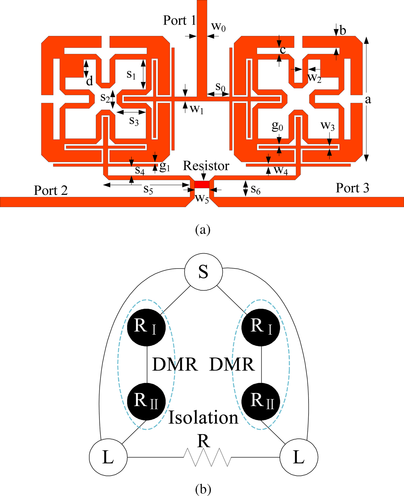
Fig. 1. (a) Configuration of the proposed power divider (b) Coupling scheme.
Analysis of the scheme of filtering power divider
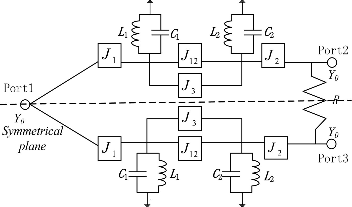
The proposed filtering power divider is a symmetrical structure. So it can be analyzed by using even- and odd-mode analysis. An equivalent-circuit model of the proposed filtering power divider is depicted in Fig. 2, which is symmetrical with respect to the symmetrical plane. The dual-mode resonator is equivalent to a LC resonator unit, where L i and C i are the self-inductance and self-capacitance, while J inverter characterizes the coupling between resonators or input/output port and resonator. Y 0 is input/output admittance.

Fig. 2. Simulated equivalent circuit of the proposed filtering power divider.
For the even-mode case, the symmetrical plane can be viewed as a magnetic wall. Figure 3(a) shows the even-mode equivalent circuit of the power divider. It can be seen that the topology of the even-mode equivalent circuit is similar to that of the second order coupled resonator bandpass filter. According to the reciprocity theorem of the two-port network, the following equation can be obtained
 $$J_1\,{\rm =}\, {{J_2} / {\sqrt 2}}. $$
Fig. 3. Equivalent circuit of the presented power divider: (a) even-mode circuit, (b) odd-mode circuit.
For the odd-mode case, the symmetrical plane can be viewed as an electric wall. Figure 3(b) shows the odd-mode equivalent circuit of the power divider, which is a one-port network. Good impedance matching can be obtained under the following condition
 $$R\,{\rm =}\, 2Z_0.$$
Analysis of the capacitance loaded resonator
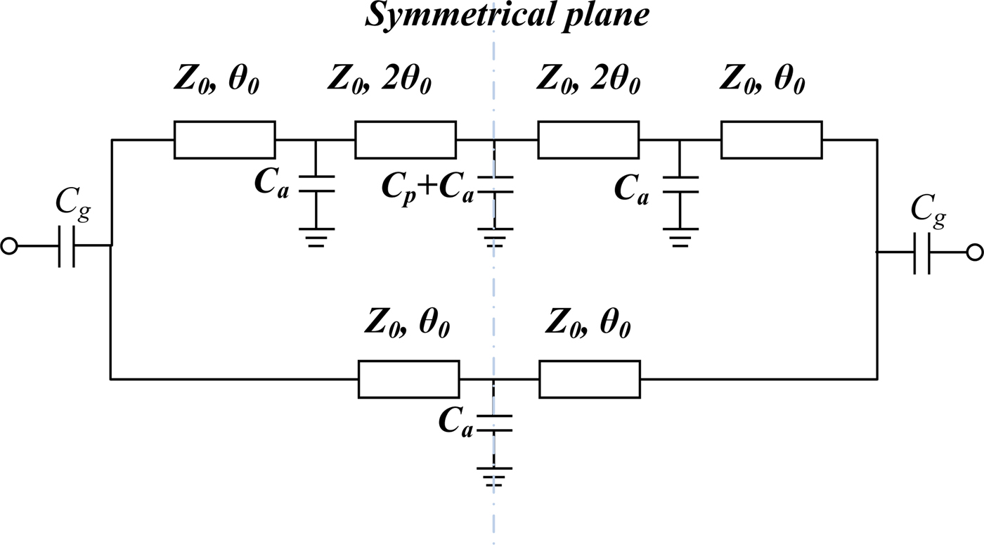
The resonator consists of four identical arms on each outer corner of square meander loop with a small patch attached to an inner corner. The two degenerate-mode resonances can be disturbed by the square perturbation element. The coupling strength is increasing as perturbation size d is increasing. Due to capacitance loaded arms, the resonator can exhibit slow-wave characteristics, which can be utilized to suppress unwanted harmonics and reduce size. Figure 4 shows the equivalent circuit model of the dual-mode resonator to better characterize its performance. C a and C p represent loaded capacitance attached to the outer corner of the resonator and the capacitive perturbation patch added in an inner corner, respectively. The characteristic impedance of the transmission line in each side of the square loop and its electric length are Z 0 and 2θ 0, respectively. Input and output coupling capacitance is equivalent to C g.

Fig. 4. Equivalent transmission-line circuit model of the resonator.
Due to the symmetrical structure, the circuit can be analyzed using odd- and even-mode analysis. For even-mode case, its input admittance Y in_even from port 1 is derived as follows
 $$Y_{in\_even} = Y_{1\_even} + Y_{2\_even},$$
where
 $$Y_{1\_even} = \displaystyle{{{{Y}^{\prime}}_{even}Z_0 + j\tan \theta _0} \over {Z_0(1 + j{{Y}^{\prime}}_{even}Z_0\tan \theta _0)}},$$
 $${Y}^{\prime}_{even} = j\omega C_a + j\displaystyle{{\omega Z_0(C_p + C_a)/2 + \tan 2\theta _0} \over {Z_0\lsqb {1-\omega Z_0(C_p + C_a)/2} \rsqb }},$$
 $$Y_{2\_even} = j\displaystyle{{\omega Z_0(C_a/2) + \tan \theta _0} \over {Z_0\lsqb {1-\omega Z_0(C_a/2)\tan \theta_0} \rsqb }}.$$
For odd-mode case, its input admittance Y in_odd from port 1 is derived as follows
 $$Y_{in\_odd} = Y_{1\_odd} + Y_{2\_odd},$$
where
 $$Y_{1\_odd} = \displaystyle{{{{Y}^{\prime}}_{odd}Z_0 + j\tan \theta _0} \over {Z_0(1 + j{{Y}^{\prime}}_{odd}Z_0\tan \theta _0)}},$$
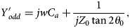 $${Y}^{\prime}_{odd} = jwC_a + \displaystyle{1 \over {\,jZ_0\tan 2\theta _0}},$$
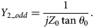 $$Y_{2\_odd} = \displaystyle{1 \over {\,jZ_0\tan \theta _0}}.$$
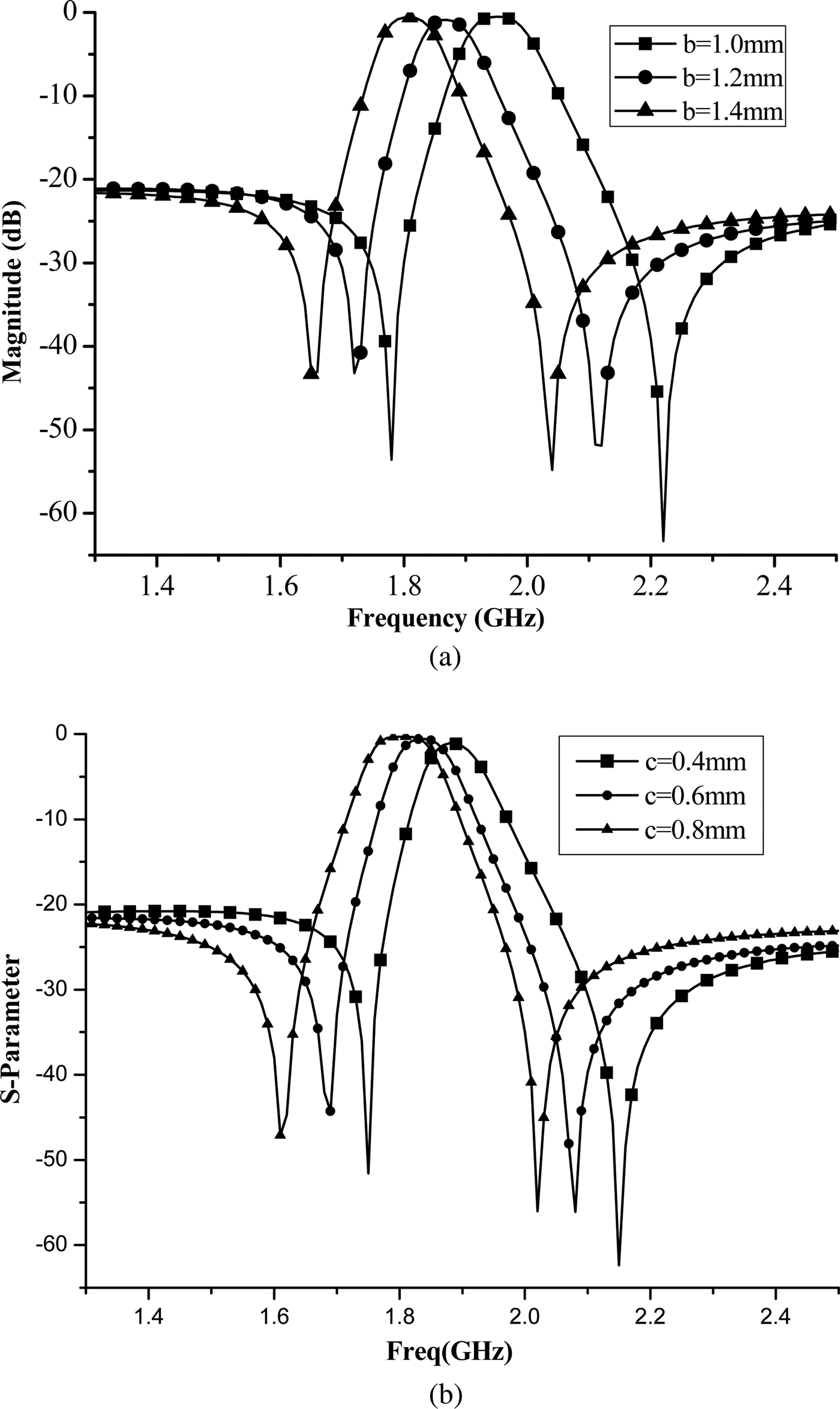
The resonator will resonate when input admittance equals to zero, which can be expressed as Y in_even = 0 and Y in_odd = 0. The loaded capacitances can change the resonance characteristics. Figure 5 shows S parameter response with varied parameters b and c, which loaded capacitances are mainly dependent on. It can be seen that the resonance can be shifted down by increasing the loaded capacitances.

Fig. 5. Simulated S parameters with varied parameters (a) b (a = 14.5 mm, c = 0.4 mm, d = 2 mm, w 0 = 1.11 mm, w 1 = 0.5 mm, w 2 = 0.6 mm, w 3 = w 4 = 0.2 mm, w 5 = 1.6 mm, s 1 = 4.5 mm, s 2 = 1.9 mm, s 3 = 3.3 mm, s 4 = 1.7 mm, s 5 = 10.6 mm, s 6 = 1.89 mm, g 0 = g 1 = 0.1 mm, R = 100 ohm) and (b) c (a = 14.5 mm, b = 1.3 mm, d = 2 mm, w 0 = 1.11 mm, w 1 = 0.5 mm, w 2 = 0.6 mm, w 3 = w 4 = 0.2 mm, w 5 = 1.6 mm, s 1 = 4.5 mm, s 2 = 1.9 mm, s 3 = 3.3 mm, s 4 = 1.7 mm, s 5 = 10.6 mm, s 6 = 1.89 mm, g 0 = g 1 = 0.1 mm, R = 100 ohm).
Simulation and experiment result
The proposed power divider was designed, simulated, and optimized using commercial software Ansoft HFSS. Modeled in the HFSS according to the circuit model given in Fig. 1(a), the specific dimensions are as follows: a = 14.5 mm, b = 1.3 mm, c = 0.4 mm, d = 2 mm, w 0 = 1.11 mm, w 1 = 0.5 mm, w 2 = 0.6 mm, w 3 = w 4 = 0.2 mm, w 5 = 1.6 mm, s 1 = 4.5 mm, s 2 = 1.9 mm, s 3 = 3.3 mm, s 4 = 1.7 mm, s 5 = 10.6 mm, s 6 = 1.89 mm, g 0 = g 1 = 0.1 mm, R = 100 ohm. The power divider was fabricated on substrate Taconic RF-35 with a relative dielectric constant of 3.5, thickness of 0.508 mm, and loss tangent of 0.0018. The circuit size of power divider is only 0.13λ g × 0.37λ g, where λ g is the guided wavelength at the center frequency. The photograph of fabricated power divider is shown in Fig. 6(a).
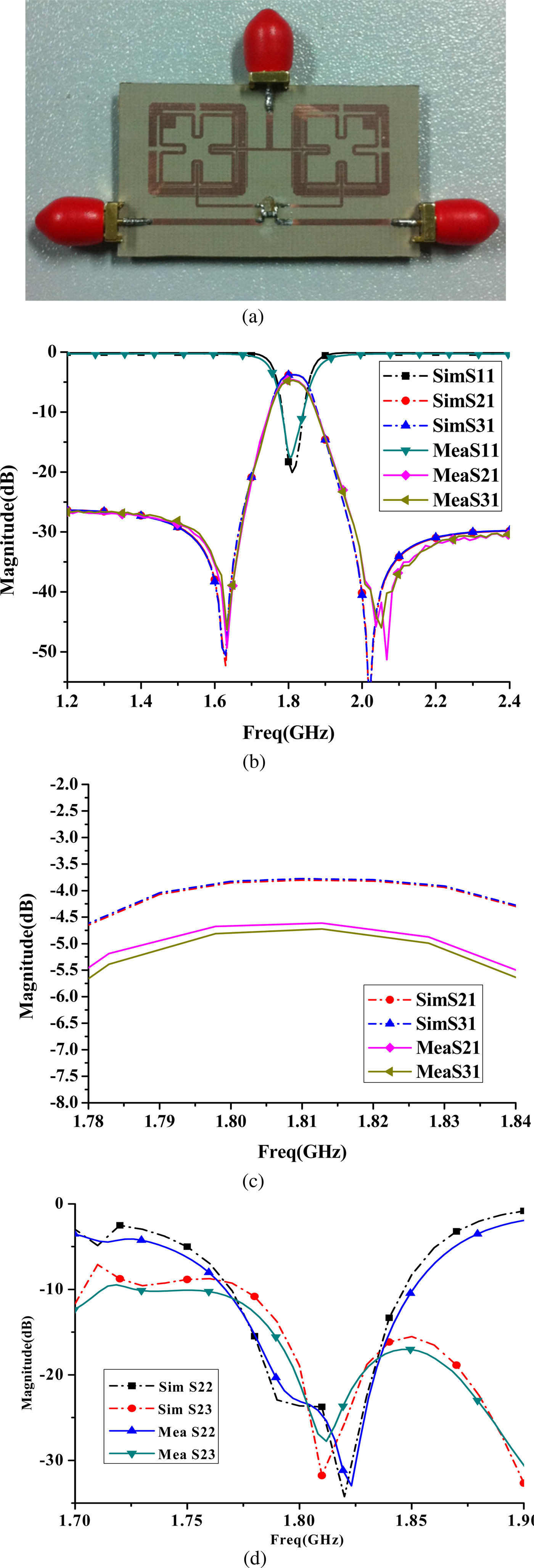
Fig. 6. Simulated and measured results of the proposed filtering power divider. (a) The photograph of fabricated power divider. (b) |S 11|. (c) |S 21|, and |S 31|. (d) |S 22|, | S 23|.
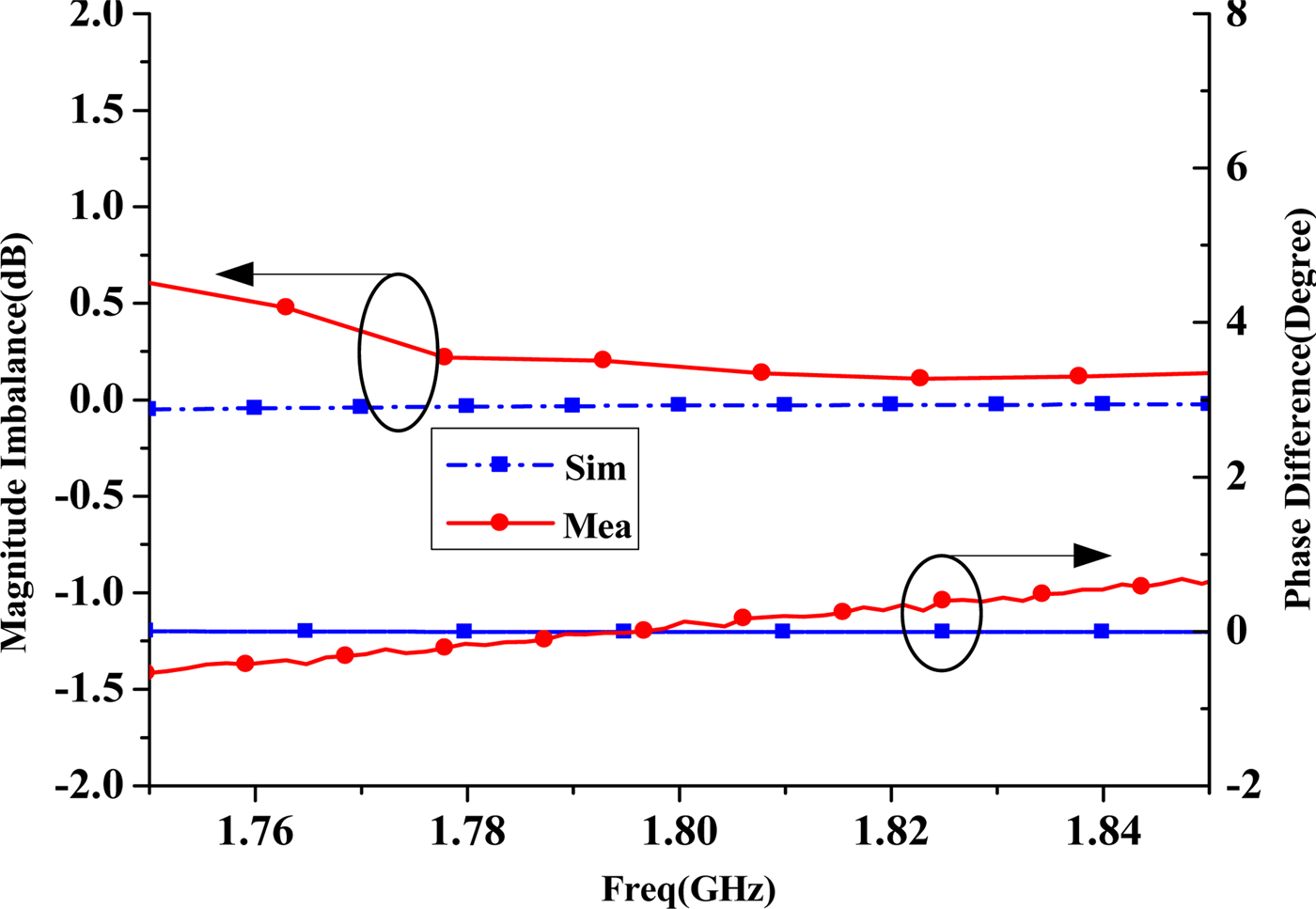
The fabricated power divider was measured using an Agilent 8757D network analyzer. Figures 6(b)–6(d) show the simulated and measured results. The passband of the proposed filtering power divider is centered at 1.8 GHz with the FBW3dB of 4.6%. There are two transmission zeroes at each side of the passband, which are located at 1.64 and 2.15 GHz, respectively. The measured passband insertion losses (|S 21| and |S 31|) are approximately 4.55 and 4.57 dB, respectively, whereas the simulated minimum insertion loss is about 3.67 dB. The difference between the measured and simulated results may be ascribed to the fabrication tolerance and assembly errors in the design. The measured input return loss is greater than 17 dB, while the measured output return loss is greater than 23 dB. In addition, the measured isolation between output ports is about 25 dB at the center frequency, as shown in Fig. 6(d). Figure 7 shows in-band amplitude imbalance and in-band phase imbalance of proposed power divider. It can be seen that in-band amplitude imbalance is less than 0.5 dB and the in-band phase imbalance is ±1°. The wide-stopband response of the filtering power divider is shown in Fig. 8. As can be seen, the measured rejection of upper stopband is greater than 25 dB up to about 4.7 GHz. Table 1 shows the comparison with some reported filtering power divider. It can be found that the filtering power divider has better performance than the referenced ones.

Fig. 7. Simulated and measured magnitude imbalance and phase difference between the two output ports.
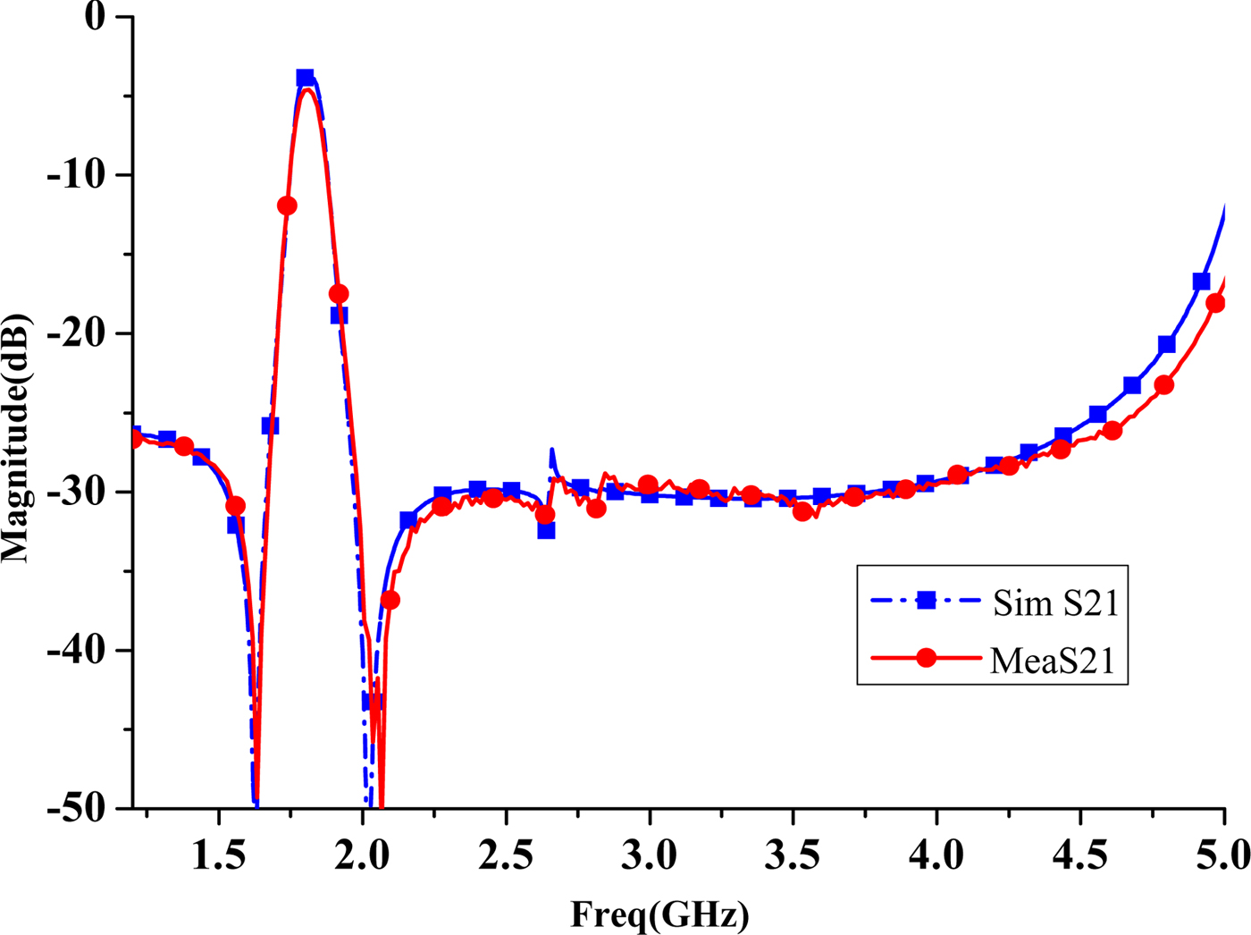
Fig. 8. Simulated and measured wide-band response of the proposed filtering power divider.
Table 1. Comparison of the proposed power divider with previous designs.

IL, insertion loss; Iso, isolation.
Conclusion
This paper presents a filtering power divider with high-performance compared with the conventional Wilkinson power divider, which includes high selectivity, high isolation, and wide upper stopband. Due to capacitive load, the resonator can exhibit slow-wave characteristics, which can be utilized to suppress unwanted harmonics and reduce size. The two degenerate-mode resonances are used to form the passband of the proposed power divider, which could generate transmission zeros at each side of the passband so as to obtain high selectivity. As a consequence, the proposed divider has the advantages mentioned above for the application in modern communication systems.
Author ORCIDs
Fei Xia, 0000-0003-3654-8775; Song Guo, 0000-0002-0271-4686.
Acknowledgement
This work was supported by the National Natural Science Foundation of China under Grant No: 61771094.
 Jiawei Li was born in Liaoning, China, in 1985. He received the B.S. degree in electrical engineering from the University of Science and Technology of China, Hefei, China, in 2008, and the M.S. degree in electromagnetic field and microwave technology from the Northwest Institute of Nuclear Technology, Xi'an, China, in 2011. He started to pursue his Ph.D. degree in electronic science and technology from University of Science and Technology of China since 2014. He has been with the Northwest Institute of Nuclear Technology since 2008. His current research interests include high power microwave transmission and radiation.
 Kaijun Song received the M.S. degree in radio physics and the Ph.D. degree in electromagnetic field and microwave technology from the University of Electronic Science and Technology of China (UESTC), Chengdu, China, in 2005 and 2007, respectively. In 2011, he received the “New Century Excellent Talents in University Award” from Chinese Ministry of Education. In 2015, he received the academic and technical leaders in Sichuan province.
Since 2007, he has been with the EHF Key Laboratory of Science, School of Electronic Engineering, UESTC, where he was a full Professor. From 2018, he is currently a full Professor with School of Electronic Science and Engineering, UESTC. From 2007 to 2008, he was a postdoctoral research fellow with the Montana Tech of the University of Montana, Butte, USA, working on microwave/millimeter-wave circuits and microwave remote sensing technologies. From 2008 to 2010, he was a research fellow with the State Key Laboratory of Millimeter Waves of China, Department of Electronic Engineering, City University of Hong Kong, on microwave/millimeter-wave power-combining technology and Ultra-Wideband (UWB) circuits. He was a senior visiting scholar with the State Key Laboratory of Millimeter Waves of China, Department of Electronic Engineering, City University of Hong Kong in November 2012. He has published more than 200 internationally refereed journal papers and conference papers. His current research fields include microwave and millimeter-wave/THz power-combining technologies; high-power solid-state microwave/millimetre -wave technologies; UWB circuits and technologies; and microwave/millimetre -wave devices, circuits and systems. Prof. Song is the Reviewer of tens of international journals, including IEEE Transactions and IEEE Letters.
 Fei Xia was born in Sichuan, China, in 1994. He received the B.S. degree from Xidian University of Electronic Technology, Xian, China, in 2017. He is currently working toward the M.S. degree in the School of Electronic Science and Technology of China, Chengdu, China. He is interested in the microwave technologies.
 Shema Richard Patience was born in Kigali, Rwanda in 1988. He received the B.Sc. degree in Electrical and Electronic Engineering from National University of Rwanda, Huye, Rwanda, in 2012 and the M.Eng. degree in Electronic Science and Technology from Beijing Institute of Technology, Beijing, China, in 2015. He joined University Of Electronic Science and Technology of China (UESTC) in 2017 where he is currently working toward the Ph.D. degree. His research interests include microwave/millimeter wave substrate integrated waveguide power dividers/combiners and passive components design in RF circuits.
 Song Guo was born in Lang Fang, Hebei Province, China, in February 1993. He received the B.Sc. degree in Microelectronics from Harbin Engineering University, Harbin, Heilongjiang, China, in 2006, and is currently working toward the Ph.D. degree in electromagnetic fields and microwave technology at UESTC (University of Electronic Science and Technology of China). His research interests include microwave and millimetre-wave power-combining technology, and microwave passive component design.
 Maoyu Fan was born in Chongqing, China, in 1991. She received the Bachelor of Science degree in physics from the University of Electronic Science and Technology of China (UESTC) in 2014, and is currently working towards the Ph.D. degree in University of Electronic Science and Technology of China. Her current research interests include microwave passive and tunable filters.