I. INTRODUCTION
In the year 2002, the Federal Communication Commission released frequency band from 3.1 to 10.6 GHz for ultra wideband (UWB) services with high data rate transmission capability (typically 100 Mbps) and Effective isotropic radiated power (EIRP) less than −41.3 dBm/MHz [1]. The wireless systems have gained a lot of popularity due to wide bandwidth, high data rate, and short-range characteristics. Thus, UWB is being used for numerous applications such as Radar, Wireless Personal Area Network (WPAN), Wireless Body Area Network (WBAN), military, and commercial applications. The antennas for the UWB system should have compact size, low-profile, low-cost, and omni-directional radiation. Abundant innate merits i.e. low-profile, light weight, easy fabrication, suitability of mass production with acceptable radiation properties of the planar monopole have instigated researchers to utilize it as UWB antenna [Reference Desmond Sim, Chung and Lee2–Reference Gautam, Yadav and Kanaujia5]. However, the range of frequency for UWB system causes an interference to the existing wireless communication system such as WLAN (5.15–5.35 GHz, 5.725–5.825 GHz), WiMAX (3.3–3.7 GHz), and ITU (8.025–8.4). Therefore, it is necessary to notch out portions of the band to avoid interference with existing wireless networking technologies [Reference Peng and Ruan6–Reference Kim and Chang9]. To overcome this problem, UWB antennas are designed with single/dual and triple stop band performance by inserting different shape structures to the UWB design [Reference Almalkawi and Devabhaktuni10–Reference Gautam and Kanaujia12]. A circular radiating patch with an embedded T-slot on the patch with a rectangular parasitic element is used to obtain ultra wide bandwidth and two ideal switches are inserted over two L-shaped parasitic elements placed in the left and right of the patch for band-notch function [Reference Sharbati, Rezaei, Shahzadi and Fakharian7]. In [Reference Emadian, Ghobadi, Nourinia, Mirmozafri and Pourahmadazar8], dual-band-notched characteristics are obtained by inserting two C-shaped structure on the back surface of the substrate. In [Reference Almalkawi and Devabhaktuni10], triple band notches are obtained using the closed loop ring resonator and in [Reference Sung11], H-shaped resonator is embedded in the radiating patch to generate triple band-notch functions. Two C-shaped slots on the radiating patch are used to generate a bandstop performance in [Reference Gautam and Kanaujia12, Reference Li, Zhai, Li, Liang and Han13]. Whereas, in [Reference Lee, Yang and Cho14], the band-notch function is achieved by inserting an Archimedes spiral-shape slot in microstrip line and in [Reference Taheri, Hassani and Nezhad15], the quarter wavelength stubs are attached in the ground plane. The modified capacitive-loaded loop (CLL) resonator beside the microstrip feed line are used for band-rejection at 3.3–3.6 GHz for WiMAX, 5.15–5.825 GHz for WLAN, and 7.25–8.295 GHz for the X-band satellite [Reference Wang, Yin and Liu16].
In this paper, the design of a compact UWB antenna with triple band-notched characteristics is proposed. The band-notched functions are obtained by attaching L- and I-shaped structures on the ground and a CLL resonator on the patch. Much wider impedance bandwidth (from 2.63 to 13.04 GHz) is obtained by using a star-like-shaped radiator and a defected rectangular ground plane. The triple band-notch rejection at WiMAX (2.9–3.7 GHz), WLAN(5.1–5.9 GHz), and ITU (7.5–8.7 GHz) is obtained by I-shape strip, CLL resonator, and flip L-shape, respectively. To validate the design, a prototype with an overall size of 25 × 20 × 1.6 mm3 is fabricated and measured. The experimental results show that the band-notched characteristic can be easily accomplished, while the antenna still preserves a simple structure, compact size, and omnidirectional radiation pattern. The Ansoft “HFSS” [17] is used for the simulation which is based on a finite-element method. The entire design and parametric study of the proposed antenna will be discussed in different sections.
II. ANTENNA DESIGN
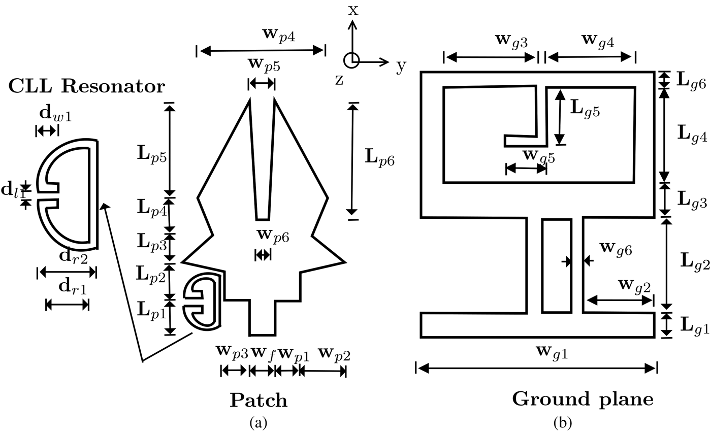
The antenna is fabricated on FR4 epoxy (ε r = 4.4 and loss tangent of 0.02) with dimensions of 25 × 20 × 1.6 mm3 as depicted in Fig. 1. The proposed antenna consists of symmetrical hand-shape structure and defected ground plane on the other side of the dielectric substrate. In place of the conventional radiator, the proposed antenna uses a star-like-shape which is formed by joining two symmetrical hands-shape geometries at lower end. The 2.4 mm wide microstrip-line is connected at the bottom of this structure to provide feeding. The conventional solid ground plane is modified to a defected ground structure by cutting one rectangular slot of 7.5 × 18 mm2 in the upper side and two rectangular slots of 7.5 × 9.5 mm2, respectively. The above discussed radiator and defected ground plane are designed to achieve UWB. Further, triple band-notch rejection at WiMAX (2.9–3.7 GHz), WLAN(5.1–5.9 GHz), and ITU (7.5–8.7 GHz) is obtained by I-shape strip, CLL resonator, and flip L-shape, respectively. The CLL structure near to the radiator is attached for band-notched characteristics at WLAN band. One I-shape strip is attached at lower rectangular slot and on flip L-shape strip is added to upper rectangular slot of the ground plane to achieve the band-notched characteristics at WiMAX and ITU bands.

Fig. 1. Schematic configuration of the proposed compact UWB microstrip antenna.
To verify the band-notched operation, the HFSS predicted current distributions at various frequencies are shown in Fig. 2. In Figs 2(b)–2(d), the simulated current distributions on radiating patch and ground plane of proposed antenna for I-, L-shaped, and CLL resonator are shown to clarify the band-notch performances. As shown in Fig. 2(b) current flows more dominant on feed line and concentrated around I-shaped strip under the lower side of the ground plane. Also in Fig. 2(c) current flows on feed line and concentrated around the CLL resonator. As shown in Fig. 2(d), the surface current density is mainly concentrated around the L-shaped strip connected in the upper slot of the ground plane. So, surface currents concentrate on the edge sides of I-, L-shaped, and CLL resonator and antenna impedance changes at these frequencies which cause band-notch properties of the proposed structures. Also high attenuation near notch frequencies are produced due to reverse direction flow of surface current in patch and feed line, which leads a cancellation of radiation fields. The current distribution of the purposed antenna at different resonant frequencies 2.75, 3.8, and 12.48 GHz are shown in Figs 2(e)–2(g) to corroborate phenomena of the UWB operation outside the band-notched frequencies. As seen in Fig. 2(e), the strong surface current flows along the radiating patch, ground plane, and feed line. It is seen that the lower frequencies are mainly agitated by left hand of the star-like radiator and middle portion of ground plane. For the 3.8 GHz operation [see Fig. 2(f)], it is observed that the surface currents are distributed uniformly over the whole radiator and ground plane. Figure 2(g) reveals that the surface current is prominent at lower corner of the ground planes, star-like radiator, and feed line.

Fig. 2. The fabricated prototype of the proposed antenna and simulated surface current distributions at band-notched centre frequencies and outside band-notched frequencies.
The proposed antenna configuration is numerically investigated and optimized using Ansoft “HFSS” electromagnetic solver. The various antenna designs during the process of triple band-notched antenna are shown in Fig. 3. The red color curve shows the ultra wide bandwidth of the antenna ranges from 2.63 to 13.04 GHz more than 10.41 GHz for VSWR less than 2.0. It is also observed that the sharp frequency band-notched characteristic is obtained very close to the desired frequency of 3.24 GHz when a I-shaped strip of 0.44 × 7.5 mm2 is attached with an antenna as shown in Fig. 3 (magenta color curve). The blue color curve in Fig. 3 shows UWB antenna with dual-band-notched characteristics obtained by adding an additional L-shaped strip in the upper slot of the ground plane. Finally, a CLL resonator is attached near to the feeding line to obtain band-notched characteristic very close to desired frequency of 5.48 GHz. CLL is a self-resonant circuit and its resonant frequency can be determined by its loop inductance and capacitance resulting from the cuts which open the loop [Reference Lin, Jin and Ziolkowski18].

Fig. 3. Simulated VSWR for I-shaped strip, L-shaped strip, and proposed structure.
Figure 4 shows the simulated results of the proposed antenna with width W g 6 of the I-shape strip, varies from 0.44 to 4.44 mm. It is observed from Fig. 4, when the value of W g 6 is increased, the rejection-band region gain increases along with the mismatching at lower frequency band and about 3.24 GHz. Therefore, it is decided on W g 6 = 0.44 mm as the optimum value with the notch rejection about 3.24 GHz.

Fig. 4. Simulated VSWR against frequency for the proposed antenna with various W g 6; other parameters are the same as listed in Table 1.
Table 1. Design parameters of the proposed compact UWB antenna with triple band-notched characteristics shown in Fig. 1.

Figure 5 shows the simulated results of the proposed antenna with lower length W g 5 of the L-shape strip, varies from 1.16 to 5.56 mm. It is observed from Fig. 5, when the value of W g 5 is increased, the rejection-band region moves toward lower frequency. Therefore, it is decided on W g 5 = 2.16 mm as the optimum value with the notch rejection about 8.07 GHz.

Fig. 5. Simulated VSWR against frequency for the proposed antenna with various W g 5; other parameters are the same as listed in Table 1.
A parametric study of the CLL element provides a necessary understanding of the interaction between the main radiator and the element. The gap between radiator and CLL resonator is kept 0.2 mm due to fabrication constraint. The CLL element is self-resonant circuit with high-Q characteristic and a compact size. Its resonance frequency can be determined by its loop inductance and the capacitances resulting from the cuts which open the loop. Therefore, it is a very suitable candidate for a band-stop filter function. The band-notched frequency is given approximately by the expression [Reference Lin, Jin and Ziolkowski18]
 $${f_{notch}}=\displaystyle{c \over {2{L_{CLL}}.\sqrt {{{\rm \epsilon }_{eff}}} }}\comma \; $$
where L CLL is the total length of the CLL element, ε eff is the effective dielectric constant, and c is the speed of the light. Thus, various numerical simulations are performed, to adjust the dimensions of the element to obtain the final design. Figure 6 shows the simulated results of the proposed antenna with length d w 1 of the CLL resonator, varies from 0.58 to 1.38 mm. It is found that when the value of d w 1 is increased, the rejection-band region moves toward lower frequency. Therefore, it is decided on d w 1 = 0.58 mm as the optimum value with the notch rejection about 5.48 GHz. Therefore, the CLL resonator can result in band-stop performance when placed near to the radiator and it can be equivalent to shunt-connected series LC resonance circuits.

Fig. 6. Simulated VSWR against frequency for the proposed antenna with various d w 1; other parameters are the same as listed in Table 1. (d r 1 = 2.2, d r 2 = 2.7, d l 1 = 0.3, and d w 1 = 0.87).
III. EXPERIMENTAL RESULTS AND DISCUSSION
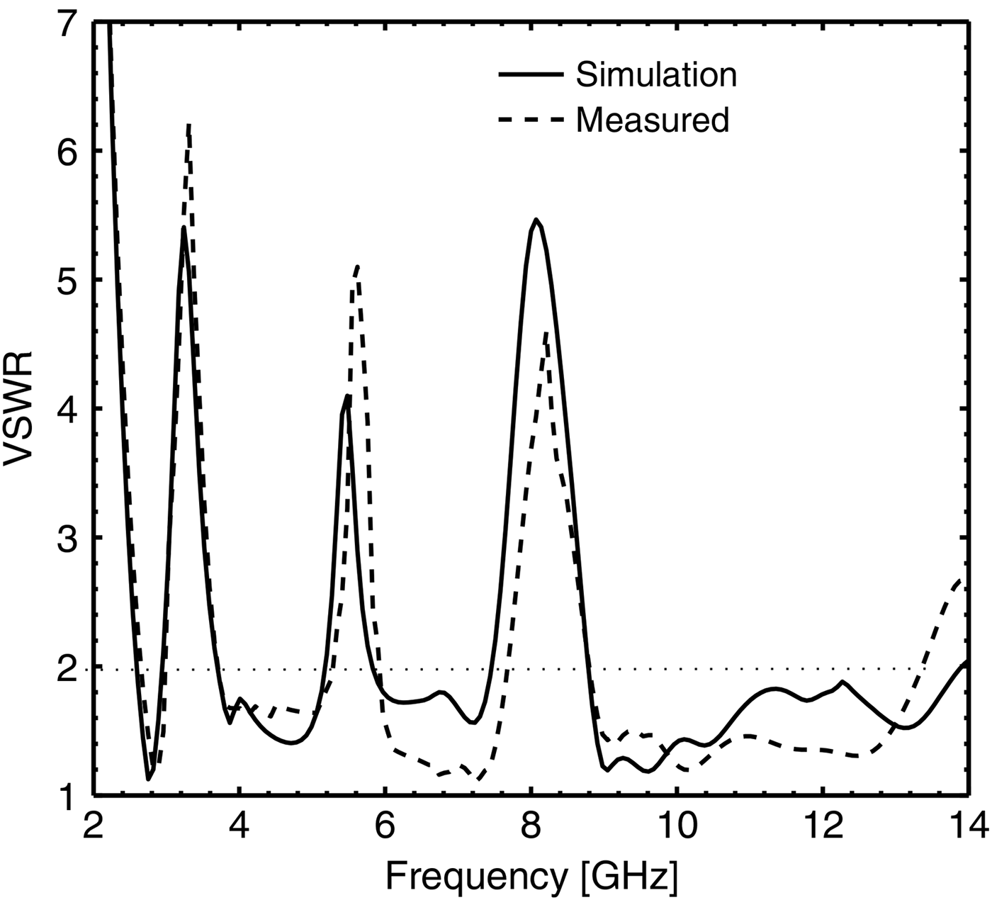
After optimizing the design using a commercially available Ansoft HFSS simulator, antenna is fabricated and measured to validate the design. The photograph of the fabricated antenna is shown in Fig. 2(a). The performance of the proposed antenna such as impedance bandwidth and radiation patterns are measured using Agilent N5230A vector network analyser. The measured and simulated VSWR curves of the proposed antenna are shown in Fig. 7. It is observed from Fig. 7 that the simulated and measured results are in good agreement. The designed antenna offers a very wide bandwidth of 10.41 GHz (2.63–13.04 GHz) with triple band-notched characteristics at WiMAX (2.94–3.7 GHz), WLAN (5.1–5.9 GHz), and ITU (7.4–8.7 GHz). The small difference between the measured and simulated results is due to the effect of SMA connector soldering and fabrication tolerance.

Fig. 7. Measured and simulated results of the compact UWB antenna with triple band-notched characteristics.
The simulated and measured peak gains of the proposed antenna across the entire operating band are shown in Fig. 8. The antenna gain remains almost constant with sharp decrease in all three notch bands as desired, that confirms the band-rejection behavior of the proposed antenna. Figures 9(a)–9(c) show the two-dimensional (2D) far-field radiation patterns in the H- and E-planes at sampling frequencies of 2.75, 3.8, and 12.48 GHz, respectively. It is found that the antenna has nearly good omnidirectional radiation patterns at all frequencies in the E-plane (xy-plane) and the H-plane (yz-plane). The radiation pattern of the antenna remains stable for entire operating band and it shows unstable radiation pattern at all three band-notches. These patterns are suitable for application in most of the wireless communication equipments, as expected.

Fig. 8. Measured and simulated gain of the compact UWB antenna with triple band-notched characteristics.

Fig. 9. Radiation patterns for various resonance frequencies for the compact UWB antenna with triple band-notched characteristics. — Measured; - - - simulated.
IV. CONCLUSION
A novel compact UWB antenna with triple band-notched characteristics for UWB applications is successfully presented and implemented. The triple band-notch rejection at WiMAX, WLAN, and ITU bands are obtained by attaching I-shape strip, CLL resonator, and flip L-shape, respectively. Effects of varying dimensions of key structure parameters on the antenna performance are also studied. The proposed antenna has several advantages, such as small size, stable radiation patterns with triple band-notched characteristics.
 Meenakshi Devi was born in Roorkee, India, on 2 July 1989. She received B.Tech. degree in Electronics and Communication Engineering from Kumaon Engineering College, Dwarahat (Uttarakhand), India in 2011 and received his M.Tech. degree in digital signal processing from G. B Pant Engineering College Pauri (Uttarakhand), India in 2014. His main research interests are design and optimization of Ultra wideband antennas.
 Anil Kumar Gautam was born in NOIDA, Uttar Pradesh, India. He received the B.E. degree in Electronics and Communication Engineering from Kumaon Engineering College, Almora, India and the Ph.D. degree in Electronic Engineering from Indian Institute of Technology, Banaras Hindu University, Varanasi, India, in 1999 and 2007, respectively. He joined the Department of Electronics & Communication Engineering, G B Pant Engineering College (GBPEC), Pauri Garhwal, India, in 2000, as an Assistant Professor and he has been an Associate Professor there since 2009. Dr. Gautam is an active member of Board of study, Academic council, and many other academic committees of GBPEC, Pauri. Dr. Gautam is also member of BOS of HNB Garhwal Central University, India and Uttarakhand Technical University, Dehradun, India. Dr. Gautam is nominated as Nodal Officer, TSP and SCSP Grants by Government of Uttarakhand and executed several projects under these grants. Dr. Gautam has supervised 15 M.Tech. and one Ph.D. Thesis and currently supervising nine Ph.D. theses in the area of Microstrip antenna. Dr. Gautam is the author/co-author of more than 70 research papers published in the refereed international journals and conferences such as IEEE, Microwave and optical Technology Letters, Springer, etc. He is the author of the 13 books in the field of Electronics Engineering in the field of Digital Electronics, Antenna and Microwave Engineering. He is a member of IEEE (USA) and many other technical societies. He is also in reviewers panel of IEEE, Transaction on Antenna and Propagation, IEEE, Antenna and Wave Propagation Letters, IET Microwaves, Antennas & Propagation, Personal and wireless communication, Springer, International Journal of Electronics, International Journal of Microwave and Wireless Technologies, International Journal of Antenna and Propagation, etc. His main research interests are in Design and Modeling of Active Microstrip Antenna, Microstrip antennas with Defected Ground Structure, Ultra wide bandwidth antennas, and reconfigurable antennas, reconfiguration antenna array, circular polarized antenna, etc.
 Binod Kumar Kanaujia currently is working as an Associate Professor in the Department of Electronics & Communication Engineering in Ambedkar Institute of Advanced Communication Technologies & Research (formerly Ambedkar Institute of Technology), Geeta Colony, Delhi. Dr. Kanaujia joined this institute as an Assistant Professor in 2008 through selection by Union Public Service Commission, New Delhi, India and served on various key portfolios, i.e. Head of Department, In-charge Central Library, Head of Office, etc. Before joining this institute he had served in the M.J.P. Rohilkhand University, Bareilly, India as Reader in the Department of Electronics & Communication Engineering and also as Head of the Department. He has been an active member of Academic Council and Executive Council of the M.J.P. Rohilkhand University and played a vital role in academic reforms. Prior, to his career in academics, Dr. Kanaujia had worked as Executive Engineer in the R&D division of M/s UPTRON India Ltd. Dr. Kanaujia had completed his B.Tech. in Electronics Engineering from KNIT Sultanpur, India in 1994. He did his M.Tech. and Ph.D. in 1998 and 2004; respectively, from the Department of Electronics Engineering, Indian Institute of Technology Banaras Hindu University, Varanasi, India. He has been awarded Junior Research Fellowship by UGC Delhi in the year 2001–02 for his outstanding work in electronics field. He has keen research interest in design and modeling of microstrip antenna, dielectric resonator antenna, left-handed metamaterial microstrip antenna, shorted microstrip antenna, ultra wideband antennas, reconfigurable, and circular polarized antenna for wireless communication. He has been credited to publish more than 105 research papers with more than 200 citations with h-index of ten in peer-reviewed journals and conferences. He had supervised 45 M.Tech. and three Ph.D. research scholars in the field of microwave engineering. He is a reviewer of several journals of international repute, i.e. IET Microwaves, Antennas & Propagation, IEEE Antennas and Wireless Propagation Letters, Wireless Personal Communications, Journal of Electromagnetic Wave and Application, Indian Journal of Radio and Space Physics, IETE Technical Review, International Journal of Electronics, International Journal of Engineering Science, IEEE Transactions on Antennas and Propagation, AEU-International Journal of Electronics and Communication, International Journal of Microwave and Wireless Technologies, etc. Dr. Kanaujia had successfully executed four research projects sponsored by several agencies of Government of India, i.e. DRDO, DST, AICTE, and ISRO. He is also a member of several academic and professional bodies, i.e. IEEE, Institution of Engineers (India), Indian Society for Technical Education, and The Institute of Electronics and Telecommunication Engineers of India.