Introduction
Radio frequency identification (RFID) is a contactless automatic method for data transfer in object identification that uses radio frequency [Reference Finkenzeller1]. A basic RFID system consists of three elements [Reference Finkenzeller1, Reference Tizyi, Riouch, Tribak, Najid and Mediavilla Sanchez2]: a tag, a reader, and a host or robot control system.
RFID is one of the fastest developing technologies, and its applications are found in more advanced areas [Reference Finkenzeller1, Reference Tizyi, Riouch, Tribak, Najid and Mediavilla Sanchez2]. This development of RFID system and its emerging application stimulated the need for solving the issues of efficiency and compactness of identification (ID) system. Since the diplexer is the most important element in the ID system, the main goal is to design a compact and highly performing diplexer.
Microwave filters and diplexers are the main components of the channel selection and signal separation in modern wireless communication systems. They reduce the operating bandwidths in the reception and emission chains. A typical full-duplex wireless communication system uses a diplexer to receive and transmit signals from/to a single antenna.
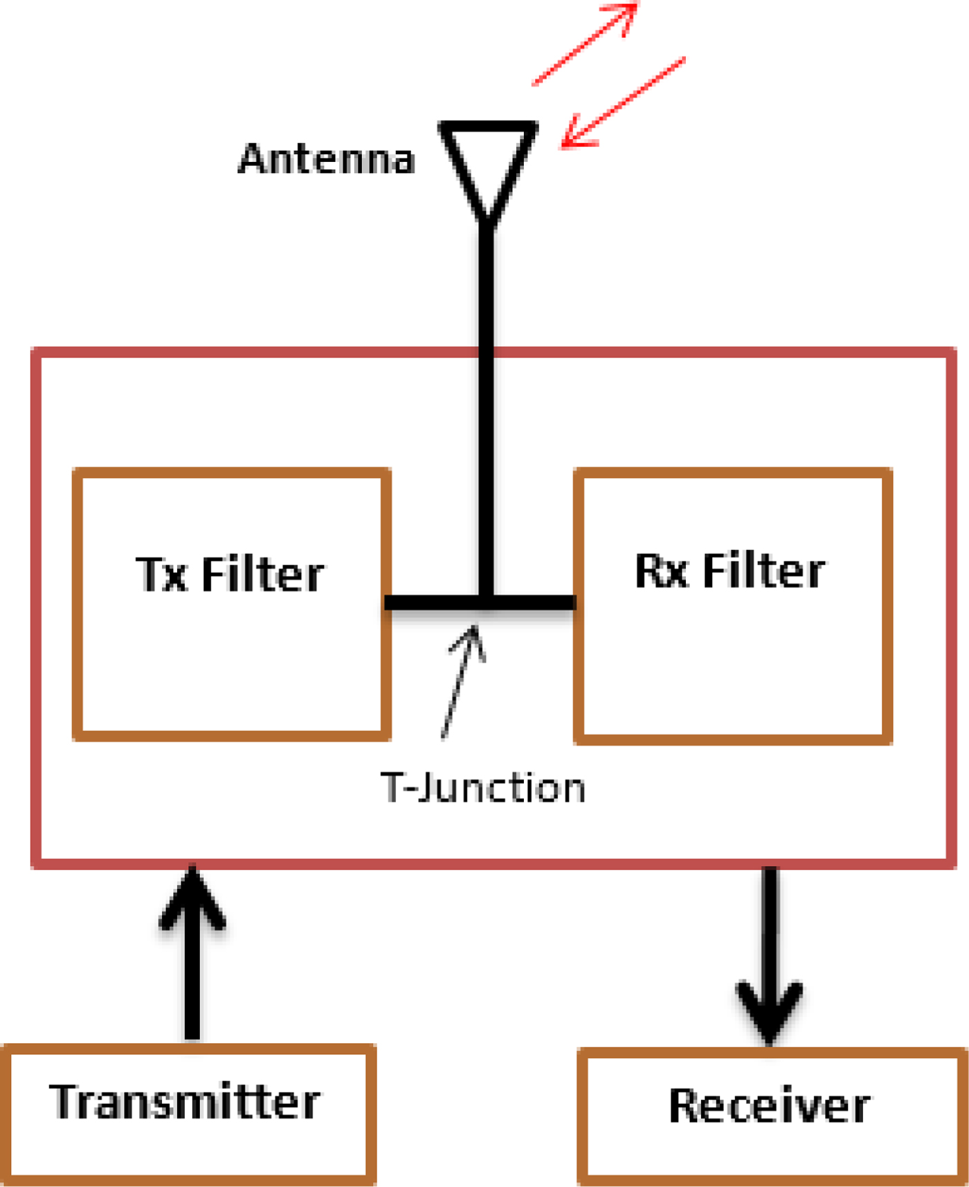
A diplexer typically comprises two filters, associated matching networks, and a combining circuit that ensures both filters match the antenna and have a good isolation between them (Fig. 1).

Fig. 1. General architecture of a diplexer with T-junction.
The T-junction and the frequency splitter are the most popular combining circuits used in diplexers. Their dimensions should be chosen carefully [Reference Konpang4, Reference Yang, Chi and Itoh5] to allow each filter to match the antenna and introduce an open circuit at the other band.In the literature [Reference Chen, Huang, Chou and Wu3, Reference Yang, Chi and Itoh6–Reference Nosrati and Atlasbaf11], there are two methods to reduce the diplexer size:
The first method uses an improved diplexer structure that combines two filters using either a common stepped impedance resonator (SIR) [Reference Chen, Huang, Chou and Wu3] or a composite right/left handed (CRLH) resonator [Reference Yang, Chi and Itoh6, Reference Lee, Wu and Itoh7]. Both resonators do not require a T-junction and, therefore allow to reduce the diplexer size. However, the impedance ratio of SIR is not significant because its T x and R x bands are too close to each other, making it impractical to use; CRLH resonators, on the other hand, have not reported resonance frequencies that are too close [Reference Nosrati and Atlasbaf11].
The second method miniaturizes both filters that make up the diplexer [Reference Chuang8–Reference Hong and Lancaster10].
As one of the regular RF and microwave components, and because of its high performance with compact size, the diplexer based on a square open-loop resonator (SOLR) filter is becoming increasingly important and widely used in RFID technology to design compact RFID readers, as well as in modern wireless communication systems [Reference Yang, Chi and Itoh6–Reference Hong and Lancaster10]. According to [Reference Hong and Lancaster10], three different types of coupling structures can be produced with SOLR: electric, magnetic, and mixed coupling (Fig. 2).

Fig. 2. Basic coupling structures of coupled microstrip SOLR. (a) Electric, (b) magnetic, (c) mixed coupling.
To design a high-performance, compact diplexer, we investigate in this paper a new type of miniature microstrip filter, based on a SOLR coupled with U-shape in input and output. We also use a T-junction as a combining circuit, because it is suitable for a diplexer system with two extremely close bands [Reference Chuang8].
Fig. 3, illustrates the steps used in this work to design the two microstrip filters that constitute the diplexer.

Fig. 3. Approach steps used to design the T x/ R x filters.
Design approach of the two filters
Definition of the specifications and calculation of the parameters of the two filters
As we described in Fig. 3, the first step in designing the two filters that make up the diplexer is to define their specifications. Figure 4(a) and 4(b) present the specifications of the T x and R x filters. The main objective in this work is to design both filters to operate at a frequency of 2.2 GHz (2.6 GHz) with a rejection >40 dB, and good attenuation in the R x and T x bands. The bandwidth is defined between F TX1 and F TX2 for the R x filter and between F TX1 and F TX2 for the T x filter (Fig. 4). The insertion losses (IL) of both filters must be <3 dB. The filters must also be compact in size and simple to realize.

Fig. 4. Specifications of the two filter: (a) T x filter, and (b) R x filter.
The desired center frequency, order of the filter, coupling factor and external quality factor (Q ext) are the main physical parameters of the filters.
The order of the filter M is calculated using the Chebychev approximation with:
 $$ M= {{arcosh^{-1}({1}/{\varepsilon}\sqrt{(10^{{A\over 10}-1}})}\over{arcosh^{-1}({W}/{W_0})}} $$
and
 $$ \varepsilon=\sqrt{10^{\displaystyle {Lar \over 10}}-1},$$
where:
• A is the isolation between the T x and R x bands at the frequency
 $f= {W \over 2}$.
•
$f_0= {W_0 \over 2}$ is the resonance frequency (f 0 = 2.45 GHz).• Lar is the maximum error (Lar=1).


Using the specifications of the two filters (Fig. 4) we found M=4.
For every resonant circuit the quality factor (Q ext) can be calculated using equation (2), [Reference Matthaei, Jones and Young12]:
 $$ {1 \over Q_{ext}}={1 \over Q_L}-{1 \over Q_U}, $$
where Q L is the loaded quality factor, which quantifies the selectivity of a resonator and Q U is the unloaded quality factor which is the intrinsic electrical performance of a resonator. Q L and Q U can be calculated using two methods: using the reflection coefficient or the transmission coefficient as described in [Reference Tizyi, Riouch, Tribak, Najid and Sennouni13]. Using the first method and the design goals mentioned in Fig. 4, the quality factor Q L, Q U, and Q ext of the two filter T x and R x are equal to 26, 44, and 63.55, respectively.
Design Steps of the two filters (T x/R x)
The first step to realize the 4th order filters is to model the input/output of the global circuit with microstrip lines (Fig. 5(a)). We set the global line length of the T x filter at L T = λ g/4 ≃ 18 mm and L T = λ g/4 ≃ 22 mm for the R x filter, then we adjust the value of N (position of the microstrip lines) to obtain the expected Q ext (Q ext = 63.55). The layout of the U-shape is presented in the Fig. 5:
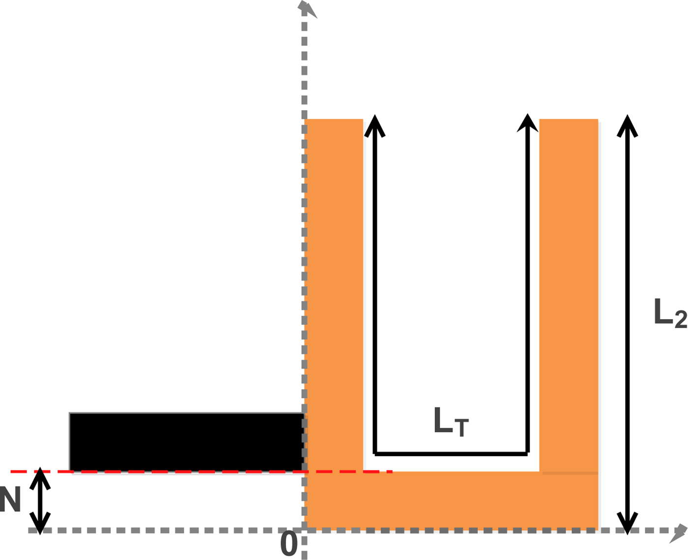
Fig. 5. The U-Shape input/output model.
Figure 6(a) and 6(b) shows the variation of quality factors as a function of N, and of the length L 2 of the U-shape, respectively. As illustrated in Fig. 6(a), the quality factor decreases when N increases, and the value of N that gives the expected Q ext is N ≃ 1.45. Setting N at 0.25 and adjusting the length L 2 of the resonator, Fig. 6(b), shows that the first value of L 2 that gives the expected value of Q ext is L 2 = 10.65 mm.

Fig. 6. The variation of the quality factor as function of: (a) N positions of the feed line (b) the length L 2 of the resonator (Fig. 5).
The second step is to study the coupling between the U-shape and the first quarter wave open-loop resonator (OLR), to find the exact value of S 1. Figures 7 and 8 show the layout of the U-shape coupling with the first OLR, and the variation of Q ext as a function of S 1.
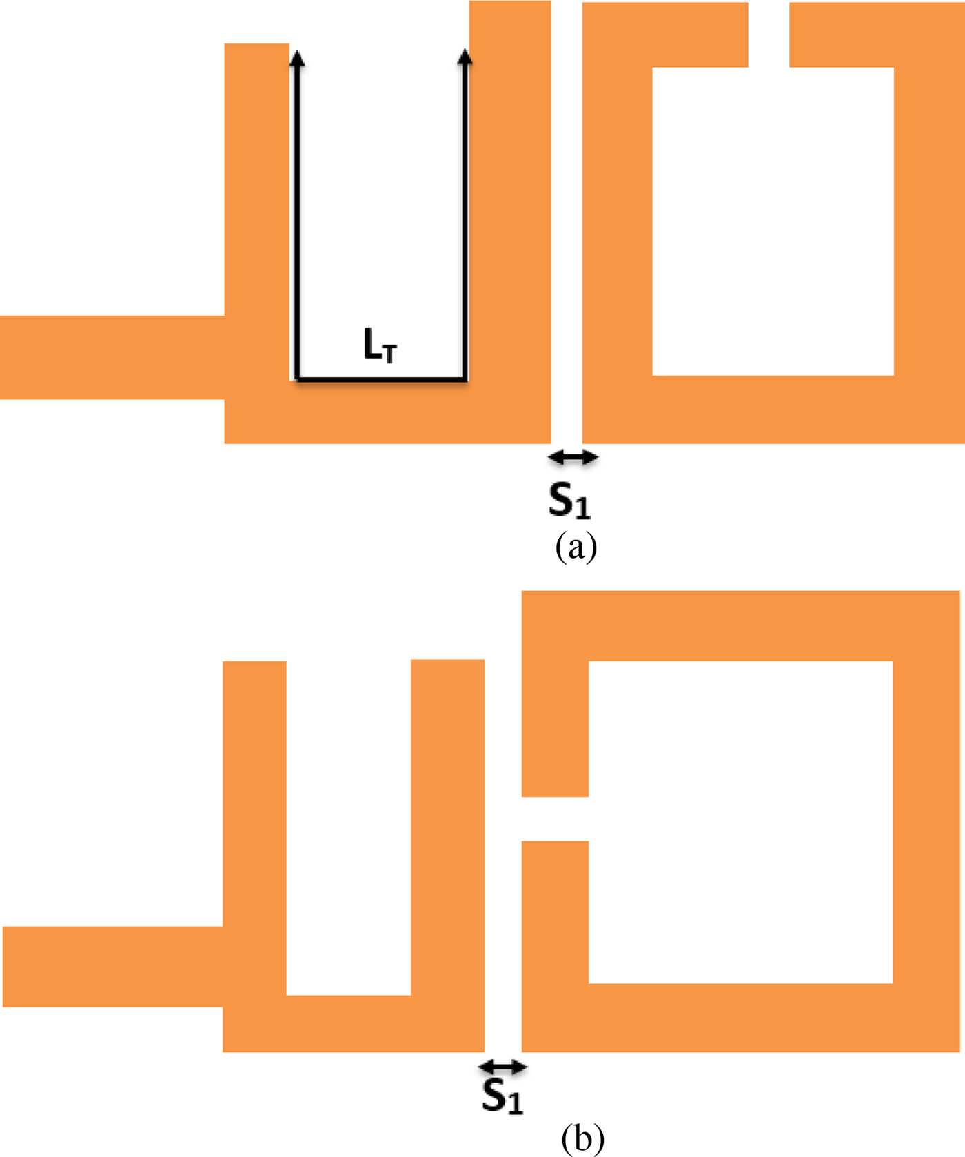
Fig. 7. The layout of the U-shape coupling with the first OLR: (a) for the T x filter (b) for the R x filter.
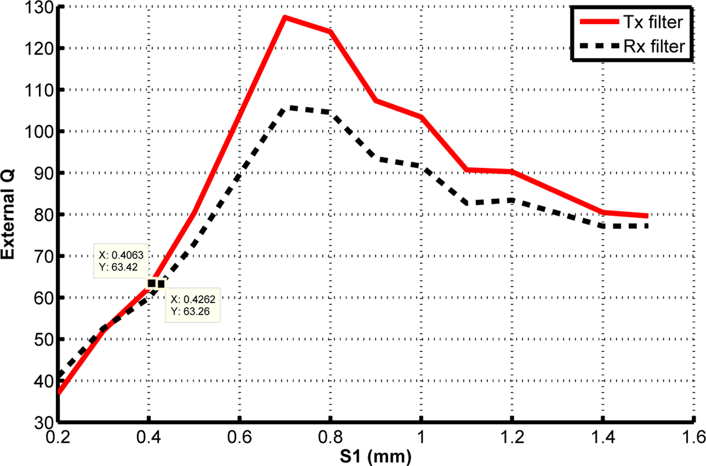
Fig. 8. The variation of the external quality factor versus S 1.
Considering Fig. 8, the best value of S 1 that gives the desired Q ext is S 1=0.4 mm for the T x filter and S 1 ≃ 0.42 mm for the R x filter. Following the same steps, we study the variation of Q ext as function of S 2 (the spacing between the first and the second OLR). Figures 9 and 10 depict the layout of the OLR, and the variation of the extracted Q ext versus S 2. The results show that the desired value of Q ext is achieved when S 2 = 0.41 mm for both filters.
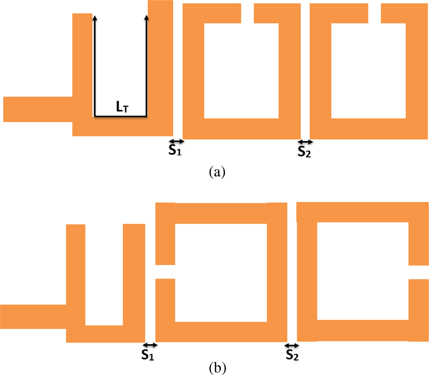
Fig. 9. The layout of the U-shape coupling with the two OLRs: (a) for the T x filter (b) for the R x filter.
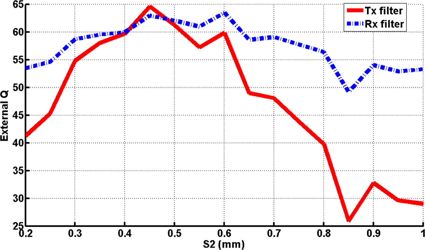
Fig. 10. The external quality factor versus S 2.
In the final step, we supposed that our filters are symmetrical, so we added the U-shape in the output with the same dimension as the input. Figure 11 shows the final design of the T x/R x filters. As we can see, in the design of the R x filter (Fig. 11(b)) we added an open two stubs in the input/output to enhance the performances of the filter [Reference Collado, Pozo, Mateu and O'Callaghan9]. The parameters of the T x and R x filters are shown in Table 1 (with S = S 1 = S 2).
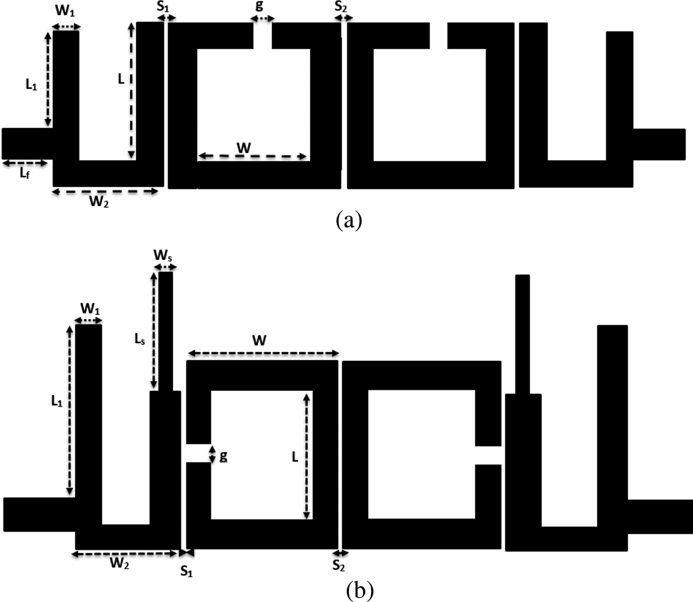
Fig. 11. The final design of the two filters: (a) T x filter, and (b) R x filter.
Table 1. Parameters of the R x/T x filters

Simulation and realization of the T x/R x filter
The filter's performance is studied by using the Advanced Design System (ADS) software. To validate the results found by ADS, we designed and simulated the same structure with High Frequency Structural Simulation (HFSS) software.
Figure 12 presents an electromagnetic response of the OLR filters, and it shows that the proposed R x/T x filters operate at 2.2/2.6 GHz respectively, with a good attenuation in the R x band (>40 dB for the T x filter), and vice versa. A good insertion loss <0.77 dB was achieved in the bandwidth. There is also a good agreement between ADS and HFSS results, as shown in Fig. 12.

Fig. 12. Comparison between ADS and HFSS simulation results (a) R x filter, (b) T x filter.
After all the design steps and optimization, the proposed OLR filters are fabricated using LPKF protomat S63. FR4 with εr = 4.4 and h = 1.58 mm is used as the substrate material. Then, it is measured experimentally using Anritsu Vector Network Analyzer. Figures 13 and 14 show the prototype of the proposed filters, and the comparison between simulated and measured results of the OLR filters. As we can see, there is a good agreement between simulated and measured results. However, there are some disagreements between simulation and measurement results, especially for the insertion loss, which can be caused by the SMA connector quality or fabrication tolerance.

Fig. 13. Photograph of the proposed filters: (a) T x filter. (b) R x filter.

Fig. 14. Simulated and measured S-parameters of the proposed filters, (a) T x filter. (b) R x filter.
Simulation and realization of the diplexer
After the simulation, and validation of results by realization and measurement of the two filters, the diplexer was formed, by connecting the two filters with the T-junction. The width and the length of its branches must be chosen carefully to get the best isolation between the T x channel and R x one (Fig. 15).

Fig. 15. T-shaped resonator.
Figure 16 depicts the layout and photograph of the compact designed diplexer. Where, both filters are connected to the same T junction to form the ISM diplexer. The T-junction dimensions were determined with Momentum EM simulator integrated into ADS. Figures 17 and 18 illustrate the simulation and the measurement results of the proposed diplexer. The results show a good insertion loss less than 0.87 dB, and isolation less than 40 dB, for the two bands T x and R x. The comparison between simulated and measured results, show a good agreement, with some disagreement in the R x band due to the fabrication error.

Fig. 16. (a) The layout, and (b) photograph of the proposed diplexer.

Fig. 17. Simulated S-parameters of the proposed diplexer, (a) adaptation (S 11, S 22) and insertion loss (S 13, S 23), (b) adaptation (S 33) and isolation (S 12).
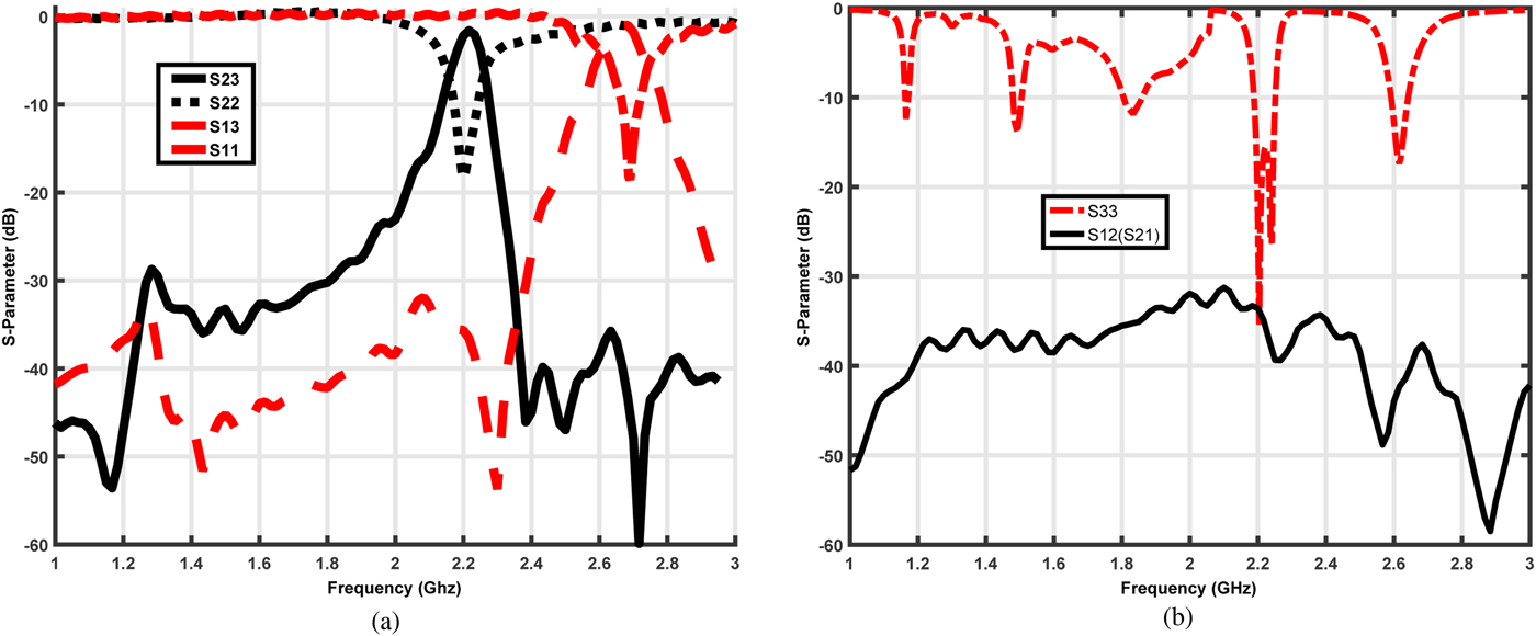
Fig. 18. Measured S-parameters of the proposed diplexer, (a) adaptation (S 11, S 22) and insertion loss (S 13, S 23), (b) adaptation (S 33) and isolation (S 12).
Table 2 compares the simulated performances of the R x filter, the T x filter, and the diplexer in terms of insertion loss, return loss, and T x and R x attenuation. The differences observed between the electrical response of the filters alone and the electrical response of the diplexer are not significant, which means the coupling phenomena between the two filters are very weak. Table 3 resumes the difference between the simulated and measured results of the two filters and the proposed diplexer. In order to emphasize the advantage of the proposed diplexer compared to previous works, we compared our diplexer results with the ones obtained in [Reference Feng, Gao and Che15–Reference Feng, Hong and Che18] (Table 4). The results show better isolation and insertion loss, and a larger bandwidth.
Table 2. Comparison in simulated performances between T x, R x filters, and diplexer

Table 3. Comparison between simulated and measured results of the T x, R x filters, and diplexer

Table 4. Comparison measured results of different diplexer

Simulation of the systems “diplexer+Antenna”
A microstrip antenna is connected to the proposed diplexer in order to evaluate its performance. Our previous work in [Reference Tizyi, Riouch, Tribak, Najid and Mediavilla14] proposed an antenna operating in the ISM band (between 2.45 and 5.48 GHz). Using this antenna as a starting point, we modified it to improve its bandwidth using the technique cited in [Reference Tizyi, Riouch, Tribak, Najid and Mediavilla Sanchez2] so that it covers both diplexer bands T x and R x.
The antenna design and its S-parameter simulation are presented in the Fig. 19. The results show that the antenna operates at frequency 2.4 GHz with a bandwidth of 0.7 GHz.

Fig. 19. (a) The antenna design and parameters (all units are in mm), and (b) The simulation results.
The antenna provides an omnidirectional radiation pattern at the 2.4 GHz, with the gain of 2.15 dB as illustrated in Fig. 20.

Fig. 20. The radiation patterns of the microstrip antenna, (a) 3D, (b) 2D.
We combined the diplexer with the antenna (Fig. 21), and we simulated the full system using CST software. Figure 22 presents the S-parameter simulation, where the system operates at 2.2 GHz when port 1 is fed, and at 2.6 GHz when port 2 is fed. The system also provides a good isolation between port 1 and port 2 (better than 30 dB).

Fig. 21. The full system: diplexer + microstrip antenna.
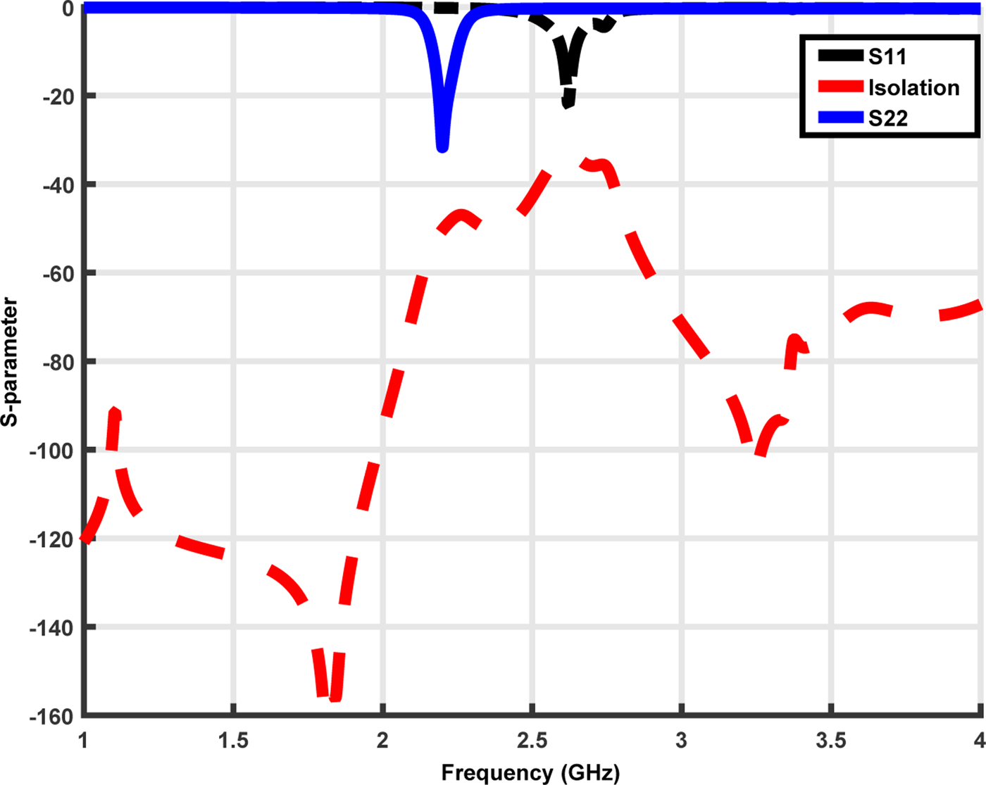
Fig. 22. The S-parameter simulation of the full system.
Conclusion
In this work we propose a simple description and an analytical method to design a compact microstrip diplexer for RFID applications, using two SOLR filters. The two filters and diplexer were designed, fabricated, and measured. In order to evaluate the diplexer's performance, it was connected to a microstrip antenna, and the full system was simulated using CST software. The results show that the microstrip diplexer has an excellent performance: low insertion loss (<0.8 dB), high isolation between the T x and R x frequency bands, and good return loss to both bands. The comparison between simulated and measured results shows a good agreement. The proposed diplexer was compared to other works, and the results show that the proposed structure provides a high isolation with a good insertion loss and wide bandwidth with a good adaptation in the two ports.
 H. Tizyi received the M.Sc. degrees in Computers, Electronics, Electrical Engineering and Automation (CEEA) from Faculty of Science and Technology, Errachida, Morocco in 2009. He received Master degree in Electronics and Telecommunication from Abdelmalek Essaadi University, Tetouan, Morocco in 2011. He is currently working toward the Ph.D. Degree in Telecom and Information Technology at National Institute of Posts and Telecommunications - INPT, Morocco. His research interests include RFID, microwave circuit, and antenna.
 F. Riouch is a professor in the National Institute of Posts and Telecommunications - INPT, Rabat, Morocco. She received her engineering degree from ENAC-France in 1983. She then prepared a Certificate of Preparation for Research in Electronics and Telecommunications from Mohammadia School of Engineering - EMI, Rabat, Morocco. She has held several leadership positions at INPT where she participates in teaching, administration and research work. Her professional interests include the area of antennas and wave propagation in mobile radio environment.
 A. Tribak received the M.Sc. degree in physics from Abdelmalek Essaadi University, Tetouan, Morocco, in 2006. He received a Master degree in communications engineering from the University of Cantabria, Santander, Spain, in 2008, and received the Ph.D. of Telecommunication degree in 2011, from the University of Cantabria, Santander, Spain. Since 2006–2011, he has been with the Department of Communications Engineering, University of Cantabria. Since 2011 he is an associate Professor in the National Institute of Posts and Telecommunications, Rabat, Morocco. His main area of activities is microwave circuits and systems; antenna feed subsystems for satellite and radio-astronomy applications.
 A. Najid has Master degrees in Networking and Communication Systems and Ph.D. thesis in Microwaves and Wireless Networking in 1997 from Institut National Polytechnique de Toulouse INPT, France. He was working as researcher Engineer at INRIA Labs from 1998 to 2000. His research fields are routing protocols, wireless networking, microwave, and antennas design. Curently, he is a full Professor at Institut National des Postes et Telecommunications in Rabat, Morocco.
 A. Mediavilla received the Doctor of Physics (Electronic) degree with honours in 1983, both from the University of Cantabria, Santander. From 1980 to 1983 he was Ingenieur Stagiere at THOMSON-CSF, France. He is currently head of the Communications Engineering Department at the University of Cantabria. He has a wide experience in the analysis and optimization of nonlinear microwave active devices. His research interests are nonlinear MESFET/HEMT and HBT device modeling with special application to the large signal computer design and new waveguide structures for antenna feed systems.