


Introduction
Emerging millimeter-wave applications require high-performance integrated components and circuits. For instance, the next generation payloads for satellite constellations [Reference Christopher1], imaging systems [Reference Vizard2], and automotive radars are in demand of highly integrated, low-cost, and high-performance alternative technologies to outperform existing systems.
Recently, novel integrated hollowed multilayer printed circuit board (PCB) technologies, using air as the main propagation medium, have been introduced. High-performance integrated components and circuits based on those promising technologies have been demonstrated. They achieve drastically reduced losses compared to their counterparts based on conventional PCB technologies. For instance, [Reference Parment, Ghiotto, Vuong, Duchamp and Wu3–Reference Tomassoni, Silvestri, Ghiotto, Bozzi and Perregrini6] reported the air-filled substrate integrated waveguide (AFSIW) technology. Al-Tarifi and Filipovic [Reference Al-Tarifi and Filipovic7] presented a nearly-rectacoax hollowed transmission line technology. Li et al. [Reference Li, Ma, Yan, Wang and Mou8] discussed the substrate integrated suspended line (SISL) technology. Those technologies are manufactured using standard PCB fabrication process including electroplating, milling, drilling, and laser cutting.
The design of high-performance millimeter-wave circuits based on those emerging technologies requires the development of novel transitions for interconnects, especially for operation at millimeter-waves. In [Reference Parment, Ghiotto, Vuong, Carpentier and Wu9], a broadband and low loss Ka-band transition between AFSIW and SISL was presented. It is based on a six-layer structure to avoid parasitic modes. In [Reference Li, Ma, Yan, Wang and Mou8], a conductor-backed coplanar waveguide (CBCPW) to SISL transition operating from DC to 8 GHz was introduced. This transition consists of three sections: a tapered CBCPW, a tapered conventional stripline, and a tapered SISL segment. Instead, in this paper, a direct transition between CBCPW and SISL is presented for operation up to 46 GHz with an experimental validation in the 0.01–50 GHz frequency range.
Transition analysis and design
As described in [Reference Li, Ma, Yan, Wang and Mou8] and [Reference Parment, Ghiotto, Vuong, Carpentier and Wu9], the SISL transmission line consists of five substrates of thickness h i (Fig. 1). The top and bottom substrates (substrates 1 and 5 shown in Figs 1(a) and 1(e), respectively) are used to enclose the air cavities made within the milled inner substrates (substrates 2 and 4 shown in Figs 1(b) and 1(d), respectively). The middle substrate 3 (shown in Fig. 1(c)) sustains the strip conductor. The thinner the middle substrate is, the lower the dielectric loss becomes. Such SISL structure was studied in [Reference Parment, Ghiotto, Vuong, Carpentier and Wu9]. The mono-mode bandwidth is limited by the fc TE10 TE10 mode cut-off frequency given by:
 $$f_{cTE10} = \displaystyle{c \over {2W_{channel}}}\sqrt {1-\displaystyle{{h_3} \over H}\left( {\displaystyle{{\varepsilon_r-1} \over {\varepsilon_r}}} \right)}, $$
where w channel is the SISL channel width, H is the SISL channel total height (H = h 2 + h 3 + h 4), ε r is the middle substrate dielectric relative permittivity, and c is the light velocity.
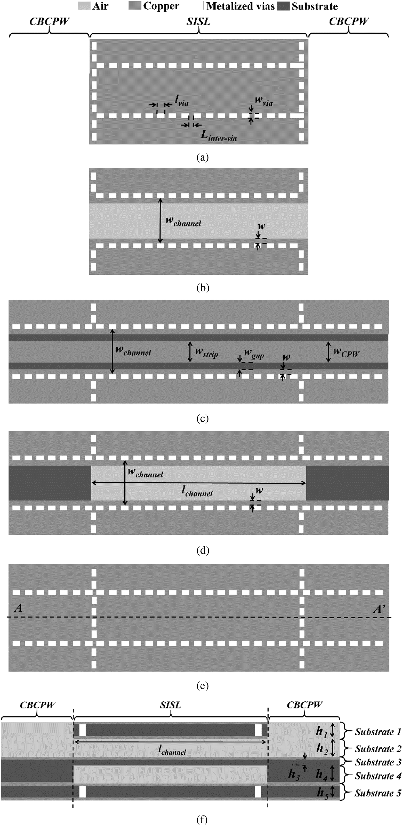
Fig. 1. Geometry of the back-to-back CBCPW to SISL transition: (a) top view of substrate 1, (b) top view of substrate 2, (c) top view of substrate 3, (d) top view of substrate 4, (e) top view of substrate 5, (f) cross-section view along the AA’ cutting line.
The geometry of the proposed transition is illustrated in Fig. 1. As shown in Fig. 1, the CBCPW is designed using two layered substrates (substrates 3 and 4). This allows achieving a 50 Ω characteristic impedance CBCPW with the conductor strip width w strip and gap width w gap dimensions identical to a 50 Ω characteristic impedance SISL, as illustrated in Fig. 1(c). In Fig. 1(b), an opened air cavity with two dielectric slabs on side walls of total width w channel is realized in substrate 2. Beneath the conductor strip, another air cavity of the same width w channel is implemented in substrate 4 as shown in Fig. 1(d). To prevent coupling from a parallel plate mode in the top substrate (substrate 1), conductive via rows are implemented as shown in Fig. 1(a).
Experimental results
For demonstration purpose, a compact back-to-back transition between CBCPW and SISL has been fabricated with Rogers RT/Duroid 6002 having a relative permittivity of ε r = 2.98 and a thickness of 0.254 mm for substrates 1, 2, 4, 5 and 0.128 mm for substrate 3. To obtain a fc TE10 above 50 GHz, an air-cavity width of w channel = 2.565 mm is obtained using (1). To obtain a 50 Ω characteristic impedance SISL, w strip is determined to be equal to 0.85 mm. After a preliminary design, the CST Microwave Studio 3D electromagnetic software has been used for simulation and fine tuning. The other prototype dimensions are w = 0.508 mm, w gap = 0.35 mm, w CPW = 0.85 mm, l channel = 26.7 mm, l via = 1.016 mm, L inter-via = 0.508 mm, and W via = 0.508 mm. Pictures of the fabricated prototype substrates are shown in Fig. 2 before assembly. The substrates 2 and 4 air cuts, shown in Figs 2(b) and 2(d), are made by a laser cutting process. For experimental validation, a 67 GHz E8391A vector network analyzer from Agilent and an SC5226 text fixture from Anritsu were used. An N7555A electronic calibration module from Keysight and a CBCPW thru–reflect–line (TRL) calibration kit, illustrated in Fig. 3, were used for calibration in the 0.01–26.5 and 26.5–50 GHz frequency range, respectively. The TRL calibration reference planes are shown in Fig. 2(d).
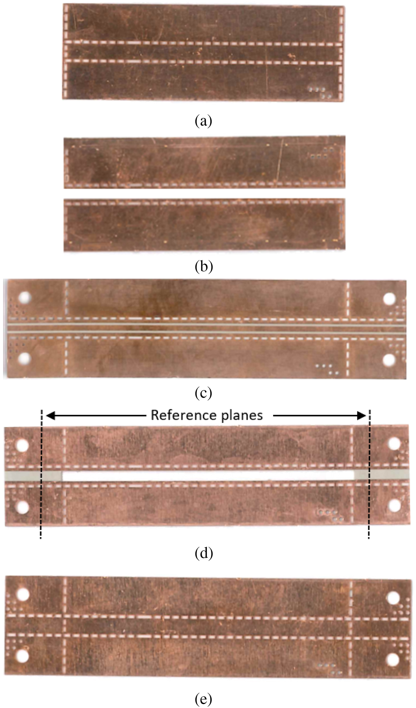
Fig. 2. Pictures of the fabricated prototype substrates before assembling: (a) substrate 1: top substrate enclosing the SISL structure, (b) substrate 2: SISL upper air cavity, (c) substrate 3: SISL and CBCPW conductor strip, (d) substrate 4: SISL lower air cavity, (e) substrate 5: bottom substrate enclosing the SISL structure.

Fig. 3. Pictures of the fabricated TRL calibration kit : (a) thru, (b) reflect, and (c) line with a delay of 6.25 ps.
Simulated and measured results are compared in Fig. 4. A good agreement between simulation and measurement results is obtained.

Fig. 4. Back-to-back transition S-parameters obtained in simulation and measurement.
A return loss of better than 10 dB is achieved up to 50 and 46 GHz in simulation and measurement, respectively. This difference is mainly due to fabrication uncertainties that may have resulted in a reduced TE10 mode cut-off frequency. From 0.01 to 46 GHz, the measured return loss is higher than 10 dB and the total insertion loss of the back-to-back transition prototype is 1.18 ± 1.02 dB. Considering the SISL transmission loss [Reference Parment, Ghiotto, Vuong, Carpentier and Wu9], it is determined that the proposed transition has 0.59 ± 0.51 dB of insertion loss in the 10 MHz to 46 GHz frequency range.
Table 1 compares the performance of the proposed multilayer transition with the CBCPW to SISL transition reported in [Reference Li, Ma, Yan, Wang and Mou8]. The proposed topology allows operation up to 46 GHz while being more compact.
Table 1. Performance comparison of the reported CBCPW to SISL transition

Bold is to highlight our results.
Conclusion
A compact multilayer transition between CBCPW and SISL for operation up to 46 GHz has been reported with an experimental validation in the 10 MHz to 46 GHz frequency range. The proposed transition is of high interest for interconnecting within the future millimeter-wave radar and communication systems based on the high-performance hollowed multilayer SISL technology.
 F. Parment was born in Rouen, France, in 1990. He received the Integrated Electronic Systems Engineer and Ph.D. degrees from the Grenoble Institute of Technology (INPG), Grenoble, France, in 2013 and 2016, respectively.
 A. Ghiotto received the M.Sc. and Ph.D. degrees (both with distinction) in microwave engineering from the Grenoble Institute of Technology, Grenoble, France, in 2005 and 2008, respectively. From 2009 to 2012, he has held a Post-Doctoral Research Associate position at the École Polytechnique de Montréal, Montréal, QC, Canada. In 2012, he joined the Laboratory of Integration from Materials to Systems (IMS), where he is currently an Associate Professor (with Full Professor habilitation). His current research interests include the analysis, design, and integration of microwave and millimeter-wave passive and active circuits in BiCMOS and CMOS technologies. Dr. Ghiotto is the TPC Chair of the 2019 European Microwave Conference (EuMC). He is an Associate Editor of the EuMA International Journal of Microwave and Wireless Technologies and a technical reviewer for several IEEE transactions and letters. Since 2017, he is the Chair of the IEEE MTT French chapter.
 T.-P. Vuong was born in Saigon, Vietnam. He received the Ph.D. degree (with the Léopold Escande award) in microwave engineering from the Institut National Polytechnique (INP), Toulouse, France, in 1999 and the HDR (Habilitation à Dériger des Recherches) degree in microwave engineering from the Institut Polytechnique de Grenoble (Grenoble INP), in 2007. From 2001 to 2008, he was an Associate Professor in microwave engineering at the School of Advanced Systems and Networks (ESISAR). Since 2008, he has been working as a Professor at the School of Engineering in Physics, Applied Physics, Electronics and Materials Science (Phelma) of Grenoble INP.
 L. Carpentier received the Ph.D. degree in electrical engineering from the University of Limoges, Limoges, France, in 2009. He is currently a Research and Development Engineer in the French Space Agency CNES, Toulouse, where he is involved with hyperfrequency passive components area.
 K. Wu received the B.Sc. degree (with distinction) in radio engineering from the Nanjing Institute of Technology (now Southeast University), China, in 1982 and the D.E.A. and Ph.D. degrees in optics, optoelectronics, and microwave engineering (with distinction) from the Institut National Polytechnique de Grenoble (INPG) and the University of Grenoble, France, in 1984 and 1987, respectively. Dr. Wu is currently a Professor of electrical engineering, Tier-I Canada Research Chair in RF and millimeter-wave engineering, and NSERC Industrial Research Chair in Future Wireless Technologies with the Polytechnique Montréal (University of Montreal), QC, Canada.


