


I. INTRODUCTION
Millimeter-wave frequencies have shown a great potential for systems that require high-data rates and high resolution. Nowadays an increasing number of applications such as automotive anti-collision radar (77–78 GHz), multi-gigabit wireless transmission (71–76 GHz, 81–86 GHz), and millimeter-wave imaging (94 GHz) have been assigned at W-band (75–110 GHz) imposing new design and fabrication challenges for the radiofrequency (RF) front-end components. W-band phase shifters are extensively used in the applications mentioned above to provide signal control. They find application in phased antenna arrays (transmission type) and reflect-array antennas (reflective type) for beam forming and beam steering. Topologies presented in the literature are typically based on switched true-time delay-lines (TTD) or periodically capacitive-loaded transmission lines distributed MEMS transmission line (DMTL) [Reference Stehle1, Reference Hung, Dussopt and Rebeiz2]. Microelectromechanical systems (MEMS) are utilized as tuning elements due to their advantages toward low insertion loss (IL) and high linearity when compared with solid-state technologies [Reference Rebeiz3, Reference Shih4]. In [Reference Stehle1], Stehle et al. demonstrated a 3-bit TTD phase shifter with a maximum phase shift of 360° and an IL of 5.7 dB at 76.5 GHz (63.2°/dB). A 3-bit DTML phase shifter with maximum phase shift of 400° and IL of 4.3 dB at 94 GHz (93°/dB) was shown in [Reference Hung, Dussopt and Rebeiz2]. Even though these topologies provide large phase variation of more than 360°, they are only suitable for applications that require discrete phase shift. In addition, they require large number of tuning components (10 and 28 switches in [Reference Stehle1, Reference Hung, Dussopt and Rebeiz2], respectively) whose number depends on the desired phase shift resolution. Furthermore, they utilize MEMS elements that are based on thin metallic capacitive bridges that might often fail to handle high RF power (>30 dBm) due to induced current densities that give rise to high localized temperatures. Reliability issues and failure mechanisms have been discussed in [Reference Rizk, Chaiban and Rebeiz5, Reference Chow, Wang, Jensen, Saitou, Volakis and Kurabayashi6]. A 4.25-bit DTML phase shifter with vertically actuated high-resistivity silicon blocks has been proposed in [Reference Somjit, Stemme and Oberhammer7] by Somjit et al. to improve RF power handling (40 dBm). In an alternative approach, materials with tunable properties such as ferroelectrics and liquid crystals have been used [Reference Mueller, Goelden, Wittek, Hock and Jakoby8, Reference Popov, Zavislyak and Srinivasan9]. The proposed topologies feature analogue phase shift and could potentially handle high levels of RF power (compared with planar-based geometries) due to the use of waveguide transmission lines. On the other hand, they are of large form factor (55 mm3 in [Reference Mueller, Goelden, Wittek, Hock and Jakoby8]), and they show high IL (4–8 dB) due to the large dielectric losses (tan δ: 0.05–0.07) of the involved materials [Reference Bulja, Mirshekar-Syahkal, James, Day and Fernandez10].
Air-filled metal waveguides are inherently advantageous in terms of low loss and high power handling when compared with planar transmission lines (coplanar waveguide (CPW), coplanar stripline (CPS), and microstrip) and for frequencies beyond a few GHz. Hence, it can be envisioned that their co-integration with MEMS tunable components may pave the way for outperforming reconfigurable devices. This concept was first introduced by Daneshmand et al. [Reference Daneshmand and Mansour11] for the application of a waveguide switch at K and Ku-bands. Later, Sammoura et al. [Reference Sammoura and Lin12] demonstrated a metalized plastic W-band phase shifter tuned by deformable membranes with a maximum phase shift of 110° and an IL of 3.5 dB (31.4°/dB) at 95 GHz. A transmission-type phase shifter based on a dielectric rod waveguide and an analogue-tunable high-impedance surface was presented in [Reference Chicherin, Sterner, Lioubtchenko, Oberhammer and Räisänen13] and showed a maximum phase shift of 32° and an IL around 7.5 dB (4.3°/dB).
In this paper, novel continuously variable transmission-type and reflective-type phase shifters are presented. They are based on ridge waveguide resonators whose center frequency is varied by MEMS actuated highly conductive rigid fingers. Preliminary results were presented by the authors in [Reference Psychogiou14] for a phase shifter with moderate performance (maximum phase shift: 46.4°, IL: 3.4 dB and figure of merit (FOM) – maximum phase variation to the maximum IL, FOM – of 13.6°/dB at 106 GHz). In this paper, the authors present an extensive description of the design, fabrication, and experimental validation of the proposed concept including optimized results that correspond to a transmission phase shift variation of 70° and a FOM of 19.5°/dB. In addition, a new design for a transmission-type phase shifter based on the coupling of two tunable resonances is also reported to improve the RF performance in terms of phase shift (134°) and FOM (55°/dB). The concept has been extended to a reflective-type phase shifter design [Reference Psychogiou, Hesselbarth, Li, Kühne and Hierold15]. A reflective-type phase shifter operating at a frequency of 107.4 GHz with a state-of-the-art performance in terms of maximum analogue phase shift (377°), IL (<3.74 dB) and FOM (101°/dB) is reported. It can be directly utilized as a phase shifting element in a reflect-array antenna or it can be transformed to a transmission-type phase shifter with a circulator or a quadrature hybrid and an additional similar reflective-type device.
The organization of this paper is as follows: Section II provides a description of the proposed phase shifting principles. In Section III, a practical realization concept for W-band applications is described and applied for the design, fabrication, and experimental validation of two different transmission-type phase shifters. In Section IV, two different reflective-type phase shifters are presented and experimentally tested as a proof of concept demonstrator.
II. PHASE SHIFTER CONCEPTS
A) Transmission-type phase shifters
A transmission-type phase shifter with a variable output phase can be readily created by a transmission line tuned by a variable shunt capacitance. Its behavior can be described by equations (1) and (2). Variation of the transmission phase is achieved by increasing C which in turn deteriorates the input reflection S 11 and transmission S 21. For a worst case input reflection around −10 dB (corresponding to a worst case transmission of −0.46 dB assuming a lossless structure), the maximum achievable phase shift is limited to 18.5° and the FOM to 40.2°/dB.
 $$S_{11} = { - y \over 2 + y}\comma \; \quad S_{21} = {2 \over 2 + y}\comma \; \quad y = 2j\pi fCZ\comma \;$$
 $$\angle \, S_{21} = - \arctan \left({\pi fCZ} \right).$$
The phase shift and FOM can be increased at the cost of reduced bandwidth if a resonant structure such as a highly coupled resonator is used. In this case, the maximum phase shift can be obtained by tuning the resonator center frequency towards lower (f L) and higher frequencies (f H) so that the worst case input reflection for all tuning states will appear at the desired center frequency f cen. Figure 1 illustrates an example of such a phase shifter at a center frequency of 100 GHz. It is constructed by a parallel-LC resonator that realizes a Butterworth passband frequency response with 2.5% fractional bandwidth. Center frequency tuning from 99.6 GHz to 100.4 GHz results in a maximum phase shift of 36.9° and a maximum FOM of 80°/dB at 100 GHz.

Fig. 1. Analytical response of a lossless transmission-type phase shifter that consists of a tunable parallel LC-resonator. (a) Input reflection (S 11). (b) Transmission (S 21). (c) Phase shift (Δᵠ). (d) Schematic diagram of a single resonator coupled to the source (S) and the load (L).
The variable transmission phase shift can be further increased if more resonances are coupled in such a way so as to create a broad tunable passband with 0.46 dB ripple at the desired center frequency (e.g. 100 GHz), Fig. 2. For the same thresholds defined above, and assuming an example of a simple structure consisting of two series cascaded resonators that realize a Chebyshev passband frequency response of 1.75% fractional bandwidth and center frequency tuning between 99.15 GHz and 100.9 GHz; the resulting output phase shift increases to 137° and the FOM to 298°/dB. Similarly, further improvement in the phase shift range can be expected if three or more resonators are utilized.

Fig. 2. Analytical response of a lossless transmission-type phase shifter that consists of two series cascaded parallel LC-resonators. (a) Input reflection (S 11). (b) Transmission (S 21). (c) Phase shift (Δᵠ). (d) Schematic diagram of two series cascaded resonators coupled to the source (S) and the load (L).
B) Reflective-type phase shifter
A reflective-type phase shifter can be constructed by adding a short at one end of a transmission-type phase shifter. It is expected that the resulting reflection phase shift is approximately twice the phase shift of the transmission-type phase shifter since the signal travels twice through the device. In fact, the transmission line section between the transmission phase shifter and the short can form another resonator by itself and depending on its length it can affect the reflection phase shift range. Figure 3 illustrates the performance of the transmission-type phase shifters of Figs 1 and 2 when cascaded with a short-circuited transmission line of length L. It is evident that the output phase shift depends on the length L and it reaches a maximum of 135° and 348° for the transmission-type phase shifter of Figs 1 and 2, respectively, if L = 0° or L = 180°. For a lossless reflective-type phase shifter, |S 11| = 1 and therefore the maximum FOM is infinite. For a practical realization including lossy resonators, the maximum FOM is finite and might not necessarily appear at the frequency of maximum phase shift. This can be attributed to the fact that when a resonator is used in the reflection mode its highest loss and maximum phase variation appear at the resonant frequency (in contrast to the transmission mode where minimum loss is obtained at the resonator center frequency), whereas it is minimized in the out of resonance area but combined with reduced phase variation. Consequently, there is a trade-off between maximum phase shift and FOM.

Fig. 3. Phase shift (Δᵠ) of a lossless reflective-type phase shifter that comprises (a) the transmission-type phase shifter of Fig. 1 and a short-circuited transmission line of length L and (b) the transmission-type phase shifter of Fig. 2 and a short-circuited transmission line of length L. Input reflection is always 0 dB and therefore omitted.
III. TRANSMISSION-TYPE PHASE SHIFTERS
A) Single-ridge phase shifter
1) TUNING CONCEPT
A transmission-type phase shifter based on the concept shown in Fig. 1 can be realized by a half-wavelength (guided wavelength) long transmission line with low characteristic impedance and variable capacitive loading, Fig. 4. A realization in waveguide technology considers the use of a ridge waveguide transmission line due to the high-field concentration beneath the ridge and two sets of highly conductive moving fingers to interact with those fields. The center frequency of the resonator depends on the waveguide cross-section, the length and width of the ridge, and the signal to ground capacitive gap g. Synchronous rotation of the fingers results in a distributed variable shunt capacitance which in turn creates a transmission phase variation in the output. The maximum achievable phase shift is limited by the increased input reflection occurring at both minimum and maximum loading states and the available capacitive loading.

Fig. 4. (a) Single-ridge phase shifter concept. For a design frequency around 96.5 GHz: w 1 = 1.5 mm, h 1 = 1 mm, w 2 = 0.6 mm, h 2 = 0.5 mm, h 3= 0.785 mm, L = 1.45 mm, d 1 = 0.15 mm, d 2 = 0.3 mm. (b) Phase shift (Δᵠ) variation for various sets of fingers deflections (α) and capacitive gaps (g).
The maximum capacitive gap variation Δg depends on the initial gap g and becomes smaller for small g. On the other hand, a small g can result in increased IL and reduced power handling due to the high electric field intensity that appears in this gap. Figure 4(b) shows the simulated phase shift of the phase shifter for various capacitive gaps and a center frequency around 96.5 GHz. The simulation is conducted with a finite element solver, HFSS. Sweeping g between 26.5 µm and 214 µm results in a phase variation between 0 and 62° and an IL around 0.83 dB (0.53 dB mismatch loss and 0.3 dB conductive loss) if gold (σ: 4.1 × 10⁷ S/m) is considered as a material for both the waveguide and the fingers. The obtained phase shift is 68% larger than the one predicted by the lumped element approximation model, Fig. 1(c). This clearly shows the distributed nature of interaction of the moving fingers and electromagnetic fields which results in an increased RF performance. It is apparent that a capacitive gap variation around 187.5 µm is required so as to achieve the aforementioned phase shift. This corresponds to fingers deflection between 0° and 8° and needs to be considered for the MEMS chip design.
2) RF-MEMS CHIP DESIGN
For the RF-MEMS chip design a tilting micro mirror approach is utilized. Figure 5 illustrates a conceptual drawing of the proposed geometry. The chip is composed of a stack of three double-side polished mono-crystalline silicon wafers. It consists of three anti-parallel oriented highly conductive rigid fingers that feature an out-of-plane tilting movement. The fingers are actuated by vertically staggered comb-drive actuators that can provide large actuation force. In order to achieve high static deflection angles (>8°) with low actuation voltage (<30 V), low stiffness SU-8 polymeric torsional springs are used to provide low restoration torque. A thin metal coating on the surface of the spring realizes the DC connections between the control voltage contact pads of the chip and the rotating parts of the comb drives.

Fig. 5. Conceptual drawing of the tilting-fingers MEMS chip. The chip size is: width: 4 mm, length: 8 mm, height: 0.66 mm. L B = 1.3 mm, and L F = 1.25 mm.
Basic design and technology aspects have been presented in [Reference Li, Kühne, Psychogiou, Hesselbarth and Hierold16] and modified for the application of the phase shifter [Reference Li, Psychogiou, Kühne, Hesselbarth, Hafner and Hierold17]. In particular, specific features that improve the RF-performance in terms of IL and FOM include:
• The use of long beams (L B) so as for the comb drive actuators to be out of the RF signal path and not to interfere with the surface currents. It is required therefore for the length of each beam (L B) to be larger than 1.15 mm, where 1.15 mm corresponds to the distance from the edge of the finger to the outer side of the waveguide wall assuming a wall thickness of 0.4 mm (minimum thickness defined by the milling process) increased by a 300 µm to accommodate for alignment tolerances and wall thickness variations.
• The effective area covered by the fingers needs to be comparable with the footprint of the half-wavelength long resonator (1.45 mm × 0.6 mm) to allow for the realization of a distributed capacitive load and therefore the dimensions of the MEMS fingers are: length L F: 1.25 mm and width d 1: 0.15 mm and d 2: 0.3 mm for the edge finger and the center fingers, respectively.
• A high static deflection up to 8° under low actuation voltage <30 V which is achieved by the use of long combs (380 µm in length), small horizontal gap between the rotor and stator combs (~3 µm) and increased number of comb fingers (140), calculated according to the design rules in [Reference Li, Psychogiou, Kühne, Hesselbarth, Hafner and Hierold17].
• Low resistivity silicon for the device and stator layer and a top metallization layer of 500 nm-thick Au (note the Au skin depth at 100 GHz is 240 nm) to minimize conductive losses created by the moving fingers when interacting with the RF signal.
3) IMPLEMENTATION AND ELECTROMAGNETIC ANALYSIS
A waveguide-MEMS phase shifter was designed for a center frequency around 98 GHz as a technology demonstrator. A conceptual drawing of the numerical model is shown in Fig. 6. It consists of the ridge waveguide resonator, the MEMS chip, and two transitions from ridge waveguide to standard rectangular (WR10) waveguide. The design of the transition is based on two series connected quarter-wavelength long transformers and was optimized for frequencies between 95 GHz and 110 GHz.

Fig. 6. (a) Conceptual drawing of the single-ridge transmission-type phase shifter. (b) Tilting fingers at 0° deflection. (c) Tilting fingers at 8° deflection.
The simulation model takes into account all geometrical and material parameters for the evaluation of the phase shifter performance. In more detail, for the waveguide upper and bottom part brass material with conductivity σ: 1.5 × 10⁷ S/m is considered. For the MEMS silicon layers, the following parameters are used: device layer: ε r: 11.9, σ: 14 000 S/m, thickness: 80 µm, stator layer: ε r: 11.9, σ: 6300 S/m, thickness: 180 µm, handle layer: ε r:10.2, σ: 10 S/m, and thickness: 400 µm (dielectric data obtained by RF characterization of individual wafer samples using a waveguide fixture).
The SU-8 polymer spring is modeled as a dielectric material with ε r: 4.2 and tan δ: 0.02 (provided by the manufacturer) and for the top metallization layer a 500 nm-thick Au-metal sheet is used with a solve-inside mesh option to accommodate for the conductive losses due to the skin-depth effect. In order to significantly reduce computational time, only half of the geometry is simulated by using a PMC-symmetry boundary since both field distribution and geometry are symmetric. Figure 7 illustrates the simulated phase shifter performance in terms of input reflection, IL, and transmission phase for various fingers deflections (α): 0–8° and ridge height (h 3): 811 µm that corresponds to a minimum capacitive gap g of 9 µm. The transmission phase at zero fingers deflection has been subtracted from these curves so as to better illustrate the phase variation. At a frequency around 98 GHz (|S 11| < –10 dB), the transmission phase grows from 0° to 63.3° with an IL between 1 dB and 3.57 dB that corresponds to a maximum FOM of 17.8°/dB. The maximum phase variation (73°) appears at a slightly higher frequency (103.5 GHz), with higher IL (4.9 dB), higher input reflection (|S 11| < –4.7 dB), and lower FOM (14.9°/dB). The frequency offset between minimum input reflection and maximum phase shift is due to the change in the passband bandwidth caused by the fingers loading (not considered for the analytical response of the lumped-element model of Fig. 1). There is always a trade-off between frequency bandwidth and maximum phase shift if low input reflection and IL is required. If, for example, a bandwidth of 2 GHz is required (98.2–102.2 GHz) then a maximum constant phase variation of 42° can be realized along the whole bandwidth with an IL between 2.8 and 3 dB and would only require a maximum MEMS deflection up to 7.8°.

Fig. 7. Simulated performance of the single-ridge transmission-type phase shifter for various sets of deflection angles. (a) Input reflection. (b) IL. (c) Phase shift.
4) FABRICATION AND ASSEMBLY
The fabrication of the tunable phase shifter involves conventional machining techniques and bulk micromachining fabrication processes. For the fabrication of the MEMS chip, a bulk silicon micromachining process is utilized as described in [Reference Li, Psychogiou, Kühne, Hesselbarth, Hafner and Hierold17]. For the fabrication of the waveguide metal parts, high precision milling is used.
Figure 8 illustrates the manufactured prototype based on a split block approach. The chip is first glued on a 5 mil RT Duroid 5880 substrate and wire-bonded to the external DC biasing lines. The substrate is then mounted on the bottom part of the fixture and centered via optical alignment. Alignment pins are used for the alignment of the waveguide blocks. In order to minimize the RF signal loss due to the lateral gaps between the MEMS chip edge and the waveguide edge (measured around 80 µm) small pieces of 25 µm-thick copper foil pads are applied (Fig. 8a).

Fig. 8. (a) Manufactured prototype of the single-ridge transmission-type phase shifter. (b) Waveguide part. (c) MEMS chip (mounted without copper foil pads).
5) MEASUREMENTS AND DISCUSSION
The static deflection of the MEMS fingers needs to be characterized prior to RF measurements so as to identify the required DC biasing for synchronous deflection of the fingers. Figure 9 depicts the calibration curves of the fingers static deflection as a function of the applied DC bias voltage characterized by a white light interferometer (fast measurement cycle). The mechanical characterization is carried out at room temperature (25 ± 1°C) with the same time step used for the RF characterization of the phase shifter in order to eliminate the influence of viscoelasticity of the SU-8 torsional spring [Reference Schoeberle, Wendlandt and Hierold18]. A maximum deflection angle of 8.25° can be obtained under a maximum biasing voltage of 27.5 V. The indicated biasing states are used for the phase shifter characterization. Although a finite number of states is shown, the deflection tuning is analogue and can take any value between 0° and 8.25° with a 0.05° precision (determined by the accuracy of the measurement setup) using a bias voltage control with 0.1 V resolution. The slightly different actuation characteristics of the two fingers as well as the 0.3° initial tilt are due to device asymmetries and fabrication-related geometry variations. Separate biasing voltages are therefore needed to synchronize the deflection of both fingers during the phase-shifter characterization.

Fig. 9. Measured deflection angle of the MEMS actuated fingers under various DC biasing voltages between 0 V and 27.5 V.
Figure 10 illustrates the measured RF performance of an assembled tunable phase shifter characterized by an Agilent 8510 network analyzer at room temperature (25 ± 1°C) with calibration planes defined at the waveguide flanges and low RF input power of approximately 1 mW. For a better illustration of the RF performance, only a finite number of biasing states is plotted. The transmission phase varies between 0° and 70° at a frequency around 98.4 GHz. For this frequency, input reflection is always below −10 dB and IL is below 3.59 dB for all biasing states. This corresponds to a maximum FOM of 19.5°/dB. The IL includes the loss of the two ridge-waveguides to rectangular waveguide transitions (which was measured in a back-to-back configuration with a separate waveguide fixture and was below 0.25 dB for the frequency range between 95 and 100 GHz). The maximum phase variation of the device was measured 74.5° at a frequency of 102.5 GHz. At this frequency, the FOM reduces to 17.4°/dB due to increased input reflection (|S 11| < –5.8 dB) and IL (4.28 dB).
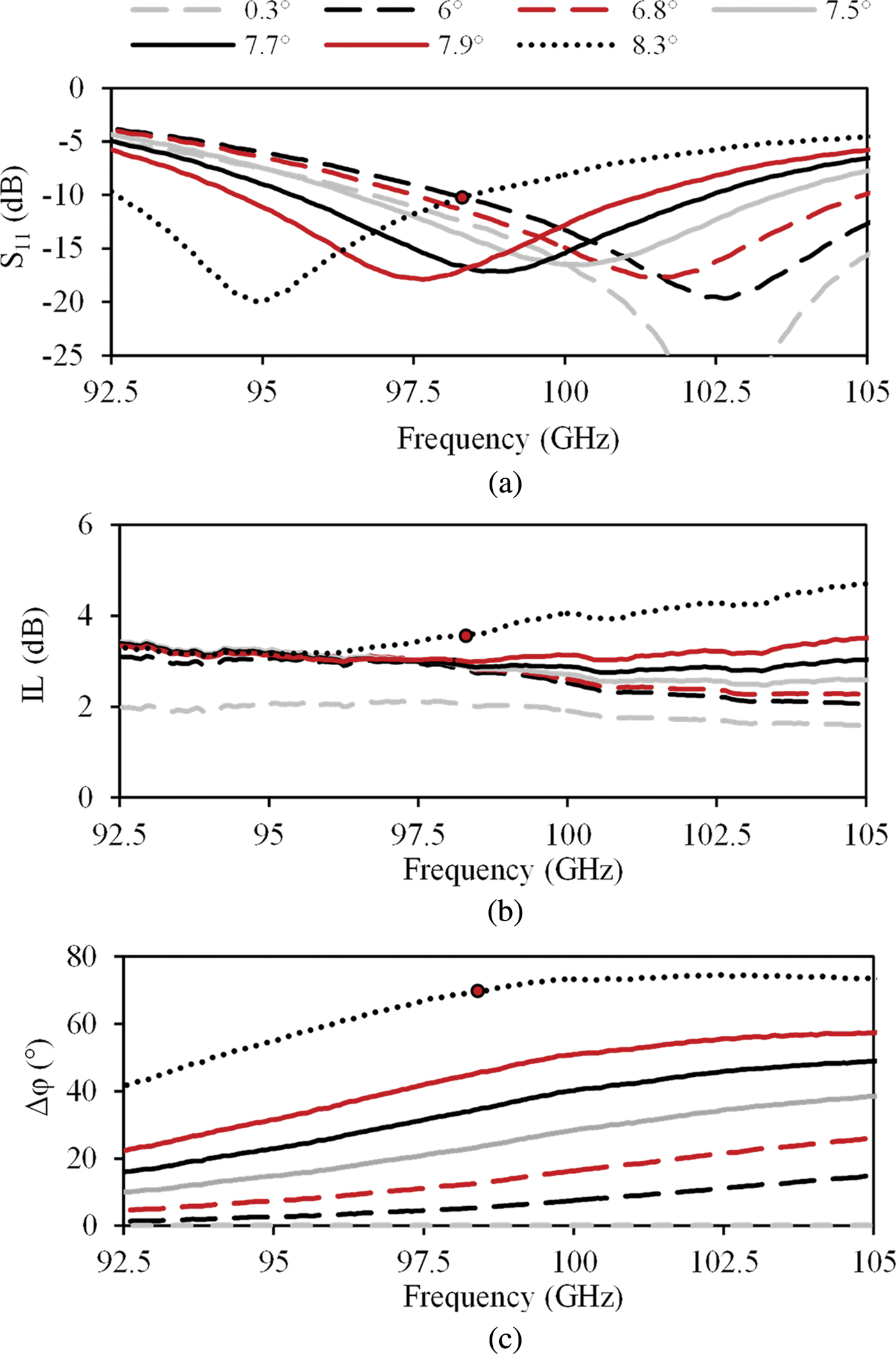
Fig. 10. Measured RF performance of the transmission-type single-ridge phase shifter for various sets of deflection angles (α) between 0.3° (DC bias: 0 V) and 8.3° (DC bias 27.5 V). The indicated deflections states are obtained using the biasing voltages shown in Fig. 9. (a) Input reflection. (b) IL. (c) Phase shift.
The measured phase shifter performance is in good agreement with the one predicted by numerical simulations (Fig. 7), even though the simulated maximum deflection was initially assigned to 8° (8.25° measured). This small discrepancy can be attributed to the fact that on the one hand deflection is larger, whereas on the other hand the ridge height (h 3 in Fig. 4) is slightly reduced with regard to the original design: 807 µm instead of 811 µm (obtained by fitting simulated to measured response), which is within the range of the fabrication tolerances (milling machine: ±5 µm). The increase of IL with deflection angle observed in both simulated and measured performance can be attributed to increased conductive losses caused by the large surface current density for smaller capacitive gaps. In addition, when the MEMS fingers are positioned at high-deflection states the current leakage to the MEMS substrate increases due to an opened air cavity below the MEMS fingers. Such a cavity acts as a discontinuity and allows the current to flow in the stator and handle layer which are made out of lossy silicon and therefore create additional loss.
B) Triple-ridge phase shifter
1) IMPLEMENTATION AND NUMERICAL ANALYSIS
A transmission-type phase shifter based on two series cascaded highly coupled resonators was designed to increase the transmission phase shift and the FOM. A conceptual drawing of the proposed geometry is shown in Fig. 11. It consists of a structured ridge waveguide that comprises three protruding studs and two separating notches and two highly conductive fingers integrated beneath the ridge.

Fig. 11. (a) Schematic drawing of the triple-ridge transmission-type phase shifter. For a design frequency around 91 GHz: w 1 = 1.5 mm, h 1 = 1 mm, w 2 = 0.6 mm, h 2 = 0.787 mm, h 3 = 0.873 mm, w e = 0.2 mm, w s = 0.3 mm, w c = 0.25 mm, d 1 = 0.15 mm, d 2 = 0.3 mm. (b) Conceptual drawing of the phase shifter model that was used for numerical simulations.
The two desired tunable resonances are created by the capacitive gap (g e) variation between the finger tips and the edge studs. Coupling of the resonances is achieved by the longer stud in the middle and the two separating notches.
The performance of the proposed structure was numerically analyzed using a finite solver HFSS and taking into consideration all geometrical and material parameters as described in Section III.A.3 and using the same MEMS chip. Optimized dimensions are given in Fig. 11 for a center frequency around 91 GHz. The design of this particular phase shifter was optimized for 91 GHz (7% lower than the single-ridge transmission-type phase shifter) due to the dimensional constraints defined by the already fabricated chip. An optimized design for 98 GHz would require a reduction of the fingers’ length and resonators’ distance.
For the particular phase shifter design, the following fabrication limitations need to be considered for the metal waveguide fabrication: maximum aspect ratio of the studs height to notch width (2.5–3), minimum notch, and stud length (200 µm). The simulated performance of the triple-ridge transmission-type phase shifter is summarized in Fig. 12. Finger deflections between 0° and 8° result in a variable phase shift between 0° and 151° at a center frequency around 91 GHz. Input reflection and IL are always below −10 dB and 2.18 dB, respectively. Such a performance corresponds to a maximum FOM of 69.3°/dB. The advantage of this design lies on the coupling of two resonances that on the one hand improve the RF performance in terms of phase shift and FOM, whereas on the other hand occupy the same volume as the previously reported phase shifter. Furthermore, the tuning of the two resonances is achieved by a single tuning element.

Fig. 12. Simulated performance of the transmission-type triple-ridge phase shifter for various sets of deflection angles. (a) Input reflection. (b) IL. (c) Phase shift.
2) MEASUREMENTS AND DISCUSSION
A waveguide fixture based on the split block approach illustrated in Fig. 8 was manufactured for evaluating the proposed concept. Figure 13 depicts the details of the fabricated waveguide part. An Agilent 8510 network analyzer was utilized to measure the phase shifter frequency response under different sets of biasing voltages. In order to better evaluate the phase shift improvement due to the series coupling of the two resonances created by the structured ridge waveguide, the RF measurements were performed with the same MEMS chip as used for the single-ridge phase shifter characterization.

Fig. 13. Detail of the fabricated waveguide part of the triple-ridge transmission-type phase shifter.
The measured RF performance of the triple-ridge phase shifter under different sets of actuation voltages is shown in Fig. 14. At 92.8 GHz, input reflection is below −10 dB for all finger states. At this frequency, the phase shifts varies between 0° and 134° and IL between 1.37 dB and 2.44 dB resulting in a maximum FOM of 55°/dB. The maximum phase variation of the device was measured around 171° at a frequency of 97.3 GHz. At this frequency, the FOM reduces to 23°/dB due to an increased IL (7.43 dB). Overall, the measured performance of this device is significantly improved when compared with the measured performance of the previously described single-ridge phase shifter and is in a good agreement with the numerical simulations shown in Fig. 12. Comparing simulations and measurements, the slight reduction in phase shift (e.g. 134° instead of 151° at 92.8 GHz) can be attributed to the capacitive gaps between the MEMS fingers and the protruding studs (g e and g c) obtained at the MEMS highest deflection state, which happen to be increased by 10 µm and 5 µm, respectively. The actual minimum capacitive gaps of the measured device have been extracted by fitting the simulated frequency response to the one obtained by RF measurements and by only changing h 2 and h 3. Such height differences are due to the fabrication tolerances of the metal blocks (~± 5 µm).

Fig. 14. Measured RF performance of the transmission-type triple-ridge phase shifter for various sets of deflection angles (α) between 0.3° (DC bias: 0 V) and 8.3° (DC bias 27.5 V).The indicated deflections states are obtained using the biasing voltages shown in Fig. 9. (a) Input reflection. (b) IL. (c) Phase shift.
IV. REFLECTIVE-TYPE PHASE SHIFTERS
Two different reflective-type phase shifters based on the previously described transmission-type phase shifters (Section III) were numerically analyzed, fabricated, and tested. Figure 15 shows the conceptual drawing of the proposed geometries and the corresponding manufactured waveguide part details.

Fig. 15. (a) Conceptual drawing of the single-ridge reflective- type phase shifter. (b) Detail of the fabricated waveguide part of the single-ridge reflective-type phase shifter. (c) Conceptual drawing of the triple-ridge reflective-type phase shifter. (d) Detail of the fabricated waveguide part of the triple-ridge reflective-type phase shifter.
A) Single-ridge reflective-type phase shifter
The single-ridge reflective-type phase shifter design is based on the same geometrical details as used for the corresponding transmission-type phase shifter. In addition, a ridge waveguide transmission line of 0.5 λg length and a waveguide short were cascaded at its end to improve the phase shift and FOM.
A single-ridge reflective-type phase shifter as detailed in Fig. 15(a–b) was numerically analyzed and manufactured. Figure 16 illustrates the measured RF performance in terms of loss and reflection-phase shift variation for a frequency band between 92.5 GHz and 110 GHz. This experiment uses the same MEMS chip and an identical set of biasing states as used for the characterization of the corresponding transmission-type phase shifter.

Fig. 16. Measured RF performance of the single-ridge reflective-type phase shifter for various sets of deflection angles (α) between 0.3° (DC bias: 0 V) and 8.3° (DC bias 27.5 V).The indicated deflections states are obtained using the biasing voltages shown in Fig. 9. (a) Loss. (b) Phase shift.
A maximum FOM of 49°/dB is measured at a frequency of 102 GHz. At this frequency, the reflection phase variation is 186° and IL is better than 3.83 dB. The maximum phase shift (191.5°) appears at 100.4 GHz with a FOM around 43°/dB. The obtained maximum phase shift and maximum FOM are significantly improved when compared with the performance of the previously reported single-ridge transmission-type phase shifter (by 157% and by 151%, respectively). This shows the advantage of coupling an additional passive resonator at the end of the transmission-type phase shifter.
B) Triple-ridge reflective-type phase shifter
In a similar way, a triple-ridge reflective-type phase shifter was designed and experimentally validated. Figure 15(c) illustrates a conceptual drawing of the numerical model. A phase shifter prototype was manufactured (Fig. 15d) and experimentally tested. Figure 17 shows the measured RF frequency response in terms of loss and reflection phase variation for a frequency band between 85 GHz and 110 GHz, which was evaluated using the same MEMS chip and sets of biasing states as in Fig. 14. The maximum FOM was measured around 101°/dB at a frequency around 107.4 GHz. At this frequency, the output reflection phase varies between 0° and 377° and the loss is always better than 3.74 dB. It is important to note here that the maximum phase variation (494°) of the phase shifter appears as expected at a lower frequency of 97 GHz (as for the corresponding triple-ridge transmission-type phase shifter). This frequency cannot be considered for the operation of the phase shifter due to the high loss of the corresponding resonators of around 14.8 dB (calculated by a fourth-order polynomial fitting of the measured data at this frequency). Thus, for a low loss and high FOM operation, the phase shifter needs to be operated toward higher frequencies between 101 GHz and 110 GHz (FOM: 77.5–85°/dB). Overall, the obtained RF performance is significantly improved when compared with the performance of the previously described phase shifters. If compared with the corresponding transmission-type phase shifter (Fig. 14) the maximum FOM is increased by 84% and the maximum phase shift by 189%.

Fig. 17. Measured RF performance of the reflective-type triple-ridge phase shifter for various sets of deflection angles (α) between 0.3° (DC bias: 0 V) and 8.3° (DC bias 27.5 V). The indicated deflections states are obtained using the biasing voltages shown in Fig. 9. (a) Loss. (b) Phase shift.
C) Comparison with the state-of-the-art
Table 1 compares the proposed phase shifter designs with several W-band phase shifter topologies already presented in the literature and each of them based on an alternative implementation concept and fabrication technology. The triple-ridge transmission-type phase shifter shows the lowest dissipated power at its nominal frequency and outperforms designs [Reference Shih4, Reference Popov, Zavislyak and Srinivasan9, Reference Sammoura and Lin12, Reference Chicherin, Sterner, Lioubtchenko, Oberhammer and Räisänen13] in terms of FOM and minimum number of tuning elements. The triple-ridge reflective-type phase shifter outperforms any other previously reported W-band phase shifter in terms of maximum FOM and minimum number of tuning elements. Its phase shift is larger than the one of designs [Reference Stehle1, Reference Shih4, Reference Somjit, Stemme and Oberhammer7, Reference Popov, Zavislyak and Srinivasan9, Reference Sammoura and Lin12, Reference Chicherin, Sterner, Lioubtchenko, Oberhammer and Räisänen13]. Design [Reference Hung, Dussopt and Rebeiz2] has larger phase shift at the nominal frequency but its IL is about 0.6 dB higher. On the other hand, it requires a large number of tuning elements (28). If both designs are compared for the same IL threshold (4.3 dB) then the phase shift variation of the triple-ridge reflective type is larger (412°). The maximum phase shift variation of design [Reference Mueller, Goelden, Wittek, Hock and Jakoby8] appears to be larger than the one of the triple-ridge reflective-type phase shifter but its loss is significantly higher at its nominal frequency. In addition, a strong magnetic field is required to tune its properties. Note that the first four designs in Table 1 describe phase shifters with a small set of discrete settings, whereas the other designs including the ones presented in this paper feature analogue/continuous control of the phase.
Table 1. Comparison of tunable W-band phase shifters.

*Transmission-type phase shifter at a nominal frequency specified by S 11<−10 dB and maximum FOM.
†Reflective-type phase shifter at a nominal frequency specified by maximum FOM.
A: analogue; D: digital; N: number of tuning elements.
V. CONCLUSION
Novel continuously variable transmission-type and reflective-type phase shifters are presented in this paper in terms of design, fabrication, and RF characterization. They are based on ridge waveguide resonators tuned by MEMS-actuated highly conductive rigid fingers directly integrated in the waveguide bottom wall. Measurements of a triple-ridge transmission-type phase shifter based on two tunable highly coupled resonators show a maximum FOM of 55°/dB and a phase shift of 134° at 92.8 GHz. By cascading an additional passive resonator and a waveguide short a reflection-type phase shifter is synthesized with large phase variation (377°), low IL (3.74 dB), and a large FOM (101°/dB) at a frequency of 107.4 GHz.
ACKNOWLEDGEMENTS
This work was supported by the Swiss National Science Foundation (SNF) under grant 200021_129832. The authors would like to thank C. Maccio, H.-R. Benedickter, and M. Lanz for their technical support, and S. Kühne for the valuable technical discussions regarding the MEMS chip fabrication.
 Dimitra Psychogiou received the Dipl.-Ing. degree in Electrical and Computer Engineering from University of Patras, Greece, in 2008. In 2008, she joined the Wireless Communication Research Group (WiCR), University of Loughborough as a research assistant. Since 2009, she has been with the Laboratory of Electromagnetic Fields and Microwave Electronics (IFH) at the Swiss Federal Institute of Technology (ETH Zurich) where she is currently working toward the Ph.D. degree. Her current research focuses on reconfigurable microwave components design, tunable filter synthesis, antenna design, and RF-MEMS.
 Yunjia Li received the B.S. degree in Electrical Engineering in 2006 from Xi'an Jiaotong University, Xi'an, China, and the M.S. degree in Electrical and Computer Engineering in 2009 from the Joint Program of Micro and Nanotechnology for Integrated Systems by Politecnico di Torino (Italy), Institut National Polytechnique de Grenoble (France), and Ecole Polytechnique Fédérale de Lausanne (Switzerland). He joined the group of Micro and Nanosystems at ETH Zurich in 2009, where he is currently working toward the Ph.D. degree. His research interests include waveguide mounted RF MEMS, comb-drive actuators, and SU-8 torsional springs.
 Jan Hesselbarth was born in Dresden, Germany, in 1970. He received the doctorate degree from Swiss Federal Institute of Technology (ETH), Zurich, Switzerland, in 2002. He worked as a design engineer with Huber + Suhner, Switzerland, from 2001 to 2005, and as a member of technical staff with Bell Labs, Dublin, Ireland, from 2005 to 2008. He then joined ETH Zurich as a Senior Researcher and Lecturer. Since 2011, Jan Hesselbarth is professor at the Institute of Radio Frequency Technology at the University of Stuttgart, Germany. His research interests are antennas and millimeter-wave circuits and packaging.
 Dimitrios Peroulis is an Associate Professor at Purdue University where he is currently leading a group of graduate students in the areas of RF MEMS, sensing, and power harvesting applications as well as RFID sensors for health monitoring of rotating machinery. He is currently a key contributor in two DARPA projects at Purdue focusing on (1) very high quality (Q > 1000) RF tunable filters in mobile form factors and on (2) developing comprehensive characterization methods and models for understanding the viscoelasticity/creep phenomena in high-power RF MEMS devices. Furthermore, he is leading the experimental program on the Center for the Prediction of Reliability, Integrity and Survivability of Microsystems (PRISM) funded by the National Nuclear Security Administration. He received the National Science Foundation CAREER award in 2008. His students have received numerous student paper awards and other student research-based scholarships. He is a Purdue University Faculty Scholar and has also received 10 teaching awards.
 Christofer Hierold has been a Professor of Micro and Nanosystems, Department of Mechanical and Process Engineering, at ETH Zurich since April 2002. Before he joined ETH Zurich he was with Siemens AG, Corporate Research, and Infineon Technologies AG in Germany. In 1990, he graduated from Technical University Munich (TUM) with a Dr.-Ing. Degree in Engineering Sciences. His research is focused on the evaluation of new materials for MEMS, on advanced microsystems, and on nanotransducers. He is Editor-in-Chief of IEEE/ASME Journal of Microelectromechanical Systems and he is a member of the International Steering Committees of Major Conferences in the field (MEMS, TRANSDUCERS, EUROSENSORS). Professor Hierold is a member of the Swiss Academy of Engineering Sciences (SATW).
 Christian Hafner got his Ph.D. at ETH Zurich for a proposition of a new method for computational electromagnetics, the Multiple Multipole Program (MMP) in 1980. This method was also the main part of his habilitation on Computational Electromagnetics at ETH in 1987. He was honored by a Seymour Cray award for scientific computing in 1990. In 1999, Christian Hafner was given the title of Professor at ETH and since 2010 he is interim head of the Electromagnetic Fields and Microwave Electronics Laboratory (IFH) at ETH. The focus of his current research is on the improvement, optimization, and generalization of numerical techniques of computational electromagnetics; the design and application of intelligent optimization procedures based on nature-inspired strategies; design and applications of metamaterials ranging from very low up to optical frequencies, photonic crystals and band gap materials, plasmonics and optical antennas, scanning nearfield microscopy, solar cells, etc. His work was published in over 100 international journals papers, as well as in seven books and book-software packages, which include his 2D-MMP, 3D-MMP, and MaX-1 codes. The latest MMP codes and 2D and 3D FDTD codes are also available in the open source package OpenMaX. Since 2005, He is organizing the annual Workshop on Numerical Methods for Optical Nano Structures at ETH.


