I. INTRODUCTION
Integrated fractional-N phase-locked loops (PLL) are important building blocks in many communication systems, both in CMOS technology [Reference Pamarti, Jansson and Galton1, Reference Pellerano, Mukhopadhyay, Ravi, Laskar and Palaskas2] and SiGe BiCMOS [Reference Herzel3, Reference Osmany, Herzel and Scheytt4]. One advantage of SiGe BiCMOS technology is the fact that SiGe HBTs are inherently radiation-hard with respect to gamma-rays, neutrons, and protons [Reference Cressler5], which makes this technology a good candidate for space applications.
Figure 1 shows an exemplary charge-pump PLL schematic, both for integer-N and fractional-N operation. In both cases, the voltage-controlled oscillator (VCO) is followed by a prescaler with a fixed division ratio of M = 2 m , where m is the number of cascaded divide-by-two circuits (DTCs). This prescaler is followed by a programmable frequency divider. Its output signal is compared with the PLL input frequency fed through a reference buffer (REF-BUF) in a phase-frequency detector (PFD). The two PFD outputs control a charge pump (CP) connected to a low-pass filter (LPF), which controls the VCO in a feedback loop. The principles of PLLs and their noise properties are described in many textbooks, e.g., in [Reference Lacaita, Levantino and Samori6]. In modern communication systems CP PLLs (type-II PLLs) are of special interest. Their infinite open-loop gain at DC results in a static phase error of zero between the two inputs to the PFD. Moreover, the PLL frequency tuning range is only limited by the VCO, that is, there is no difference between hold range and capture range as in traditional mixer-based type-I PLLs. The main disadvantage of integer-N PLLs as depicted in Fig. 1(a) is their limited loop bandwidth resulting from the limited input frequency f REF . For a given channel spacing Δf at the VCO output, the input frequency obeys f REF ≤ Δf/M. The low loop bandwidth limits the PLL settling time and prevents the VCO phase noise from efficient high-pass filtering. The solution to this problem is the fractional-N PLL, where channel spacing and loop bandwidth are decoupled. Here, the division ratio N is not constant, but is dithered around a fractional number. This can formally be described by a perfect fractional-N divider superimposed by quantization noise. The basic idea for obtaining a high spectral purity is to shape this noise such that it has most of its energy at large frequency offsets, where it can be filtered by the LPF. This can be achieved by using a ΔΣ modulator (DSM) [Reference Miller7–Reference De Muer and Steyaert9]. In [Reference Osmany, Herzel and Scheytt4] and [Reference Heyer10], the value of the fractional number was controlled by a serial–peripheral interface as indicated in Fig. 1(b). Fractional-N PLLs have the potential to reduce the phase noise significantly by using a high input frequency. However, they create a number of new problems such as fractional spurs related to the quantization noise in the DSM and quantization noise folding due to nonlinearities of the PFD/CP phase detector (PD) [Reference Riley, Filiol, Du and Kostamovaara8–Reference Wan, Swaminathan and Galton11]. Moreover, the noise coupling within a silicon chip can result in near-integer boundary spurs. They are not related to the quantization noise in the DSM, but result simply from the fact that the VCO output signal and the reference input signal may have a long common period [Reference Brennan, Wang, Jian and Radmore12]. Coupling of the high-frequency VCO signal to the reference input buffer through the common silicon substrate or through bondwires causes a VCO modulation, which may result in large in-band spurs. Mitigation of these problems is mandatory for making fractional-N PLLs with integrated VCOs a possible candidate for flexible payloads in future satellite communication systems [Reference Heyer10].

Fig. 1. Synthesizer architecture using a charge pump PLL. (a) Integer-N PLL architecture; (b) fractional-N PLL architecture.
The rest of the paper is organized as follows. Section II describes the main causes for phase noise and spurs in integer-N and fractional-N PLLs. Here, in addition to the classical topics such as device noise and quantization noise in the DSM, problems associated with signal integrity are addressed. Section III briefly outlines methods of noise reduction for each of these noise causes, and Section IV concludes this paper.
II. ORIGIN OF PHASE NOISE AND SPURS
A) Device noise
Each building block of the PLL introduces phase noise. By adding their output noise power spectral densities (PSD) weighted with their noise transfer functions results in the total PLL output phase noise spectrum [Reference Lacaita, Levantino and Samori6, Reference Herzel, Osmany and Scheytt13]. The main contributors are typically the reference phase noise at low frequency offsets, noise in reference input buffer and CP at medium offset, and VCO noise at large offsets.
The CP activity in a fractional-N PLL is higher than for the integer-N counterpart. This is due to the higher CP duty cycle α
CP
= T
ON
/T
REF
, where T
ON
is the CP activation time and T
REF
is the reference period. The PSD of the CP output current due to thermal noise and shot noise is proportional to α
CP
, whereas 1/f noise is proportional to
 $\alpha _{CP}^2 $
[Reference Lacaita, Levantino and Samori6]. Adding the two noise contributions, we obtain for the PSD of the CP output current [Reference Herzel, Osmany and Scheytt13]:
$\alpha _{CP}^2 $
[Reference Lacaita, Levantino and Samori6]. Adding the two noise contributions, we obtain for the PSD of the CP output current [Reference Herzel, Osmany and Scheytt13]:
 $$S_{CP} (f) = S_{CP}^{white} {\kern 1pt} \alpha _{CP} {\kern 1pt} \left( {1 + \displaystyle{{\alpha _{CP} f_{\rm c}} \over f}} \right){\kern 1pt}, $$
where f
c
is the 1/f noise corner frequency of the transistor. The parameter
 $S_{CP}^{white} $
corresponds to the CP current noise PSD due to white noise sources at 100% CP duty cycle. Since in a binary weighted CP
$S_{CP}^{white} $
corresponds to the CP current noise PSD due to white noise sources at 100% CP duty cycle. Since in a binary weighted CP
 $S_{CP}^{white} $
is proportional to the CP peak current I
CP
, we can introduce a figure of merit γ
CP
for the CP architecture by
$S_{CP}^{white} $
is proportional to the CP peak current I
CP
, we can introduce a figure of merit γ
CP
for the CP architecture by
 $S_{CP}^{white} = \gamma _{CP} {\kern 1pt} I_{CP} $
. Transforming the noise current PSD to the PFD input and neglecting 1/f noise, we obtain for input-referred phase PSD
$S_{CP}^{white} = \gamma _{CP} {\kern 1pt} I_{CP} $
. Transforming the noise current PSD to the PFD input and neglecting 1/f noise, we obtain for input-referred phase PSD
 $$S_{CP}^{in} = \displaystyle{{(2\pi )^2} \over {I_{CP}}} \gamma _{CP} {\kern 1pt} \alpha _{CP} {\kern 1pt}. $$
Next, we consider the reference input buffer. We assume a CMOS inverter chain as input buffer driven by a sinusoidal signal of peak amplitude V 0. The contribution of the first CMOS inverter to the input-referred phase noise can be approximately described by [Reference Herzel, Osmany and Scheytt13]:
 $$S_{BUF}^{in} \propto \displaystyle{1 \over {g_m V_0^2}} $$
where g m is the transconductance. The proportionality constant can be obtained by circuit simulation or by PLL phase noise measurements using small input amplitudes, where this noise contribution is maximized. The expressions (2) and (3) will be helpful for phase noise optimization.
B) Quantization noise
The quantization noise generated by the DSM is folded in the nonlinear PD composed of PFD and CP before it is filtered by the LPF. This effect results in an increased in-band noise floor. The PD linearity can be improved significantly by adding a DC offset current I OS between the CP output and VSS or VDD [Reference Chien14]. In this case, either only the UP current or only the DOWN current of the CP varies in the steady state, and a good matching of UP and DOWN currents is not required. With such a static phase offset, the PD characteristic can be approximated by a second-order polynomial [Reference Herzel, Osmany and Scheytt13]
 $$I = K_{PD} {\kern 1pt} \left( {\phi + \displaystyle{\beta \over 2}{\kern 1pt} \phi ^2} \right),$$
where
 $$K_{PD} = dI/d\phi = I_{CP} /(2\pi ),$$
is the PD gain and
 $$\beta = (d^2 I/d\phi ^2 )/K_{PD}, $$
is the normalized curvature of the PD characteristic at the bias point. The two-sided PD output current PSD reads for Gaussian quantization noise [Reference Herzel, Osmany and Scheytt13]
 $$S_{i,QNF} = \displaystyle{{K_{PD}^2 \beta ^2 \sigma _{\phi, in}^4} \over {2f_{REF}}}, $$
where σ ϕ,in is the standard deviation of the phase error at the PD input. Transforming S i,QNF to the PD input and from there to the PLL output, we obtain the corresponding PLL phase noise contribution given by
 $$S_{\phi, QNF} (f) = \displaystyle{{\beta ^2 \sigma _{\phi, in}^4} \over {2f_{REF}}} \vert H(f) \vert ^2, $$
where |H(f)|2 ≈ (MN)2 below the loop bandwidth. This expression has been verified by time-domain simulation in [Reference Kucharski, Herzel and Kissinger15]. The predicted dependencies on β and σ ϕ,in were also confirmed, both for phase noise and for fractional spurs.
C) Coupling spurs in fractional-N PLLs
If in a PLL the VCO is integrated, its spectral purity may be affected by coupling between different circuit blocks through bondwires and the common silicon substrate. This may cause spurs at frequency offsets equal to twice the reference frequency. Moreover, in the case of a fractional-N PLL large in-band spurs are observed resulting from modulations of the PD input by VCO leakage.
Let us consider a reference input buffer composed of a cascade of CMOS inverters. This buffer produces a current through the bondwires for ground and supply with twice the input frequency, since the inverters draw current both at the rising edge and the falling edge of the digital signal. The currents in these bondwires may couple to the VCO bondwires through the mutual inductances between REF-BUF and VCO. As a result, the VCO frequency will be modulated with 2f REF . A similar effect is observed in the CP, if the CP currents are very large. Here, the coupling spurs occur at an offset equal to ± f REF . Unlike the classical reference spurs they cannot be reduced by the LPF.
As shown in [Reference Brennan, Wang, Jian and Radmore12] and [Reference Osmany, Herzel and Scheytt4] the role of noise aggressor and noise victim may be reversed in a fractional-N PLL. The high-frequency VCO output signal may propagate to the reference input buffer and cause modulation spurs. Here, the VCO leakage can propagate through neighboring bondwires of different PLL blocks or through the common silicon substrate. The position of the largest spurs is determined by the distance of Mα from the nearest integer number, where α is the fractional part of the division ratio N. For example, for M = 4 and α < 1 the classical fractional spurs occur at ±αf REF , but the modulation spurs occur at ±4αf REF . This makes it easy to distinguish between spurs related to quantization noise and the modulation spurs, provided that the feedback divider contains a prescaler, i.e., M > 1.
Substrate noise is especially troublesome in CMOS technology. As described in [Reference Herzel and Razavi16], a noisy VCO substrate voltage modulates the transistor capacitances in the VCO. Moreover, the transistor transconductances are modulated through the body effect. The sensitivity of the VCO frequency with respect to the substrate noise can be quantified by an according VCO gain K sub = df 0/dV sub in hertz per volt. Let S V,sub (f) be the one-sided substrate voltage PSD. Since the phase represents the integrated frequency, we obtain for the corresponding phase noise spectrum
 $$S_{\phi, sub} (f) = \displaystyle{1 \over 2}S_{V,sub} (f)\left( {\displaystyle{{K_{sub}} \over f}} \right)^2 {\kern 1pt}. $$
The factor 1/2 results from the fact that the phase noise spectrum is defined as a two-sided PSD.
III. MITIGATION OF PHASE NOISE AND SPURS
In this section, we will briefly describe the methods of reducing phase noise and spurs based on the results from Section II.
A) Device noise
A high quality factor of the resonator in the VCO is essential for a low phase noise. Moreover, the intrinsic voltage amplitude should be maximized. By using a binary weighted array of switchable capacitors the analog VCO tuning range can be reduced, which also improves the phase noise [Reference Osmany, Herzel and Scheytt4]. For more details the reader is referred to the extensive literature available, such as the books [Reference Lacaita, Levantino and Samori6, Reference Hegazi, Rael and Abidi17] and the references therein.
Next, we turn to the minimization of the in-band phase noise plateau. According to [Reference Herzel, Osmany and Scheytt13], the main contributors to the phase noise plateau are typically the white noise sources in the CP (thermal noise, shot noise), the reference input buffer noise and, in the case of fractional-N PLLs, the quantization noise folded in the nonlinear phase detector. As evident from (2), a high CP current minimizes the phase noise contribution of the devices in the CP. This has been verified in a 10 GHz CMOS PLL [Reference Hu, Osmany, Scheytt and Herzel18]. Figure 2 shows the phase noise spectrum of the 10.5 GHz PLL for different CP currents. As predicted by (2), the lowest phase noise is obtained for the highest CP current of 8 mA. This does not necessarily mean that the CP must have a very high power consumption, since the duty cycle α CP is usually on the order of 10% in fractional-N PLLs and much smaller in integer-N PLLs.

Fig. 2. Measured PLL phase noise at 10.5 GHz for different CP currents [Reference Hu, Osmany, Scheytt and Herzel18]. DC offset current at the CP output is disabled.
Another main phase noise contributor may be the reference input power. When realized as a CMOS inverter chain, the first inverter should have a large g m as evident from (3). Based on extensive investigations in the context of [Reference Hu, Osmany, Scheytt and Herzel18], [Reference Heyer10], and [Reference Osmany, Herzel and Scheytt4], we recommend an aspect ratio W/L on the order of 100 for the MOSFETs in the input inverter. The following inverters may use smaller transistors, since they are less sensitive to additive noise due to the large signal slopes at their inputs.
B) Quantization noise f REF
The minimization of quantization-noise-related phase noise and spurs is based on (8). In the following, we will discuss the effect of the reference frequency, the PD nonlineariy parameter β and the PD input rms phase error σ ϕ,in on the levels of folded quantization noise and in-band spurs.
Since the total division ratio M N is proportional to 1/f REF for a given output frequency, we conclude from (8) that doubling f REF reduces this type of phase noise by 9 dB. The input frequency is usually limited by the speed of the CMOS DSM to 100–200 MHz, depending on the technology node. Moreover, the availability of crystal oscillators may limit the reference frequency for low-cost applications. A CMOS frequency doubler or quadrupler may be useful here [Reference Ng, Fischer, Feger, Stuhlberger, Maurer and Stelzer19].
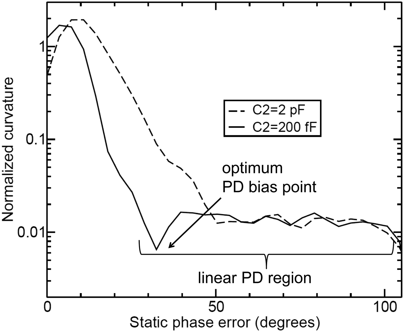
Figure 3 shows the simulated curvature β for a typical PLL as a function of the static phase error ϕ at the PFD input. This curve was obtained as follows: we performed an open-loop simulation for a cascade of PFD, CP and LPF driven by two CMOS signals with a time delay t
d
between them. The CP output current I(t) was averaged over one reference period T
REF
to obtain the mean CP current I, which depends on the input delay t
d
. A parametric simulation with respect to t
d
was performed to calculate the function I(t
d
) with a high accuracy. Finally, we have numerically calculated the second derivative of I(t
d
) to obtain the curvature parameter β from (6) as a function of the PFD input phase error ϕ = 2π(t
d
/T
REF
). As evident from Fig. 3, the linearity depends on the value of the bypass capacitor C2 placed between CP output and chip ground. This shows that a codesign of CP and LPF is important for a good PLL phase noise performance. The optimum choice of the DC phase offset at the PD input results from a trade-off between PD linearity and CP device noise. For our example, the optimum phase offset is around 36°, corresponding to a CP duty cycle of
 $\alpha _{CP} = 10\% $
. A detailed comparison of different CPs in a 130 nm SiGe BiCMOS technology was presented in [Reference Kucharski and Herzel20]. It was shown that with a sufficient DC offset at the CP output only one type of transistors is switching in the steady state. This can be a pMOSFET, an nMOSFET or a SiGe-HBT. The basic idea to maximize the PD linearity is to use the fastest available transistor for steady-state switching. In a CMOS technology this would be an nMOSFET, and in a SiGe-BiCMOS technology it would be a SiGe-HBT. In either case, a DC UP current at the CP output to VDD is preferable over a DOWN current to ground to achieve this desired behavior.
$\alpha _{CP} = 10\% $
. A detailed comparison of different CPs in a 130 nm SiGe BiCMOS technology was presented in [Reference Kucharski and Herzel20]. It was shown that with a sufficient DC offset at the CP output only one type of transistors is switching in the steady state. This can be a pMOSFET, an nMOSFET or a SiGe-HBT. The basic idea to maximize the PD linearity is to use the fastest available transistor for steady-state switching. In a CMOS technology this would be an nMOSFET, and in a SiGe-BiCMOS technology it would be a SiGe-HBT. In either case, a DC UP current at the CP output to VDD is preferable over a DOWN current to ground to achieve this desired behavior.

Fig. 3. Simulated PD nonlinearity parameter β according to (6) for two different values of the loop filter bypass capacitor C2.
A reduction of the rms phase error σ ϕ,in at the PFD input by a factor of two reduces the folded quantization noise by 12 dB according to (8). Remember that this result requires a DC phase offset between the two PFD input signals. Moreover, the curvature β should be relatively constant as obtained in Fig. 3 for large phase offsets to make the parabolic approximation (4) a reasonable assumption.
The minimization of σ ϕ,in requires small phase excursions of the divided VCO signal. As shown in [Reference De Muer and Steyaert9], single-loop DSMs have lower phase excursions than multi-stage noise shaping (MASH) DSMs, resulting in a lower in-band phase noise. Another method to minimize this type of phase noise is the maximization of the programmable divider speed. For a given total division ratio M N, a high N implies a low M. Note that the elimination of one DTC in the prescaler reduces σ ϕ,in by a factor of two. As a result, both phase noise and fractional spurs due to quantization noise folding are reduced by 12 dB [Reference Herzel, Borngraeber, Ergintav and Kissinger21].
C) Coupling spurs in fractional-N PLLs
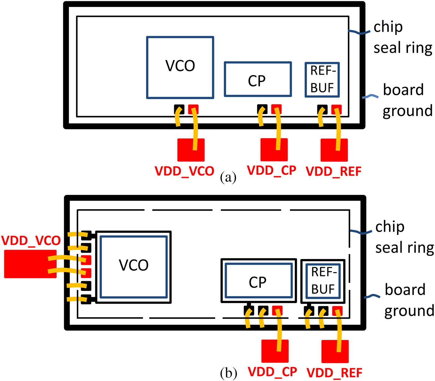
The mutual inductances between bondwires may influence the spectral purity of the PLL output signal, both in a negative and in a positive way. Figure 4 shows two examples of a PLL layout. In Fig. 4(a) the VCO is located relatively close to the CP and the reference input buffer. The bondwires of VCO, CP, and REF-BUF are in parallel, resulting in large mutual inductances between them. By contrast, in Fig. 4(b) VCO and CP are better separated from each other. Moreover, the VCO bondwires are orthogonal to the other bondwires, which minimizes the mutual inductances between them. Note that the pads for supply and ground for each block are next to each other, which maximizes the mutual inductance between them. Since they are carrying the opposite current, the total bondwire inductance for each building block is minimized. To obtain an intuitive understanding, assume that the bondwires for supply and ground are merged into one wire. In this case, the net current in this wire is zero and no voltage modulations are induced on the chip.

Fig. 4. Possible locations of PLL building blocks. (a) Example with strong noise coupling; (b) example with reduced noise coupling.
In Fig. 4(b) several layout aspects for reducing the on-chip coupling are illustrated. They are based on a long experience in developing fractional-N PLLs for mobile base stations [Reference Osmany, Herzel and Scheytt4] and for space communication [Reference Heyer10]. First of all, the VCO must have a separate supply and a separate ground on the chip. Moreover, on a low-doped silicon substrate as used for low-noise PLLs the spatial separation of the VCO from CP, reference input buffer and other digital circuitry reduces the coupling. Usually, a chip is surrounded by a seal ring, which is contacted to the substrate. If this seal ring is completely closed, the substrates of VCO and noisy building blocks are shorted, and the effect of spatial separation is partially compensated. To avoid such a ‘noise highway’, the seal ring should be broken as indicated in Fig. 4(b). Guard bands may be realized as p + doped substrate taps connected to ground. Their bondpads must not be on-chip connected to any active ground. The admittance from the noise aggressor (or victim) to the board ground through the guard band should be low. At high frequencies this implies a low bond inductance. Therefore, several bondwires for the VCO guard band may be helpful.
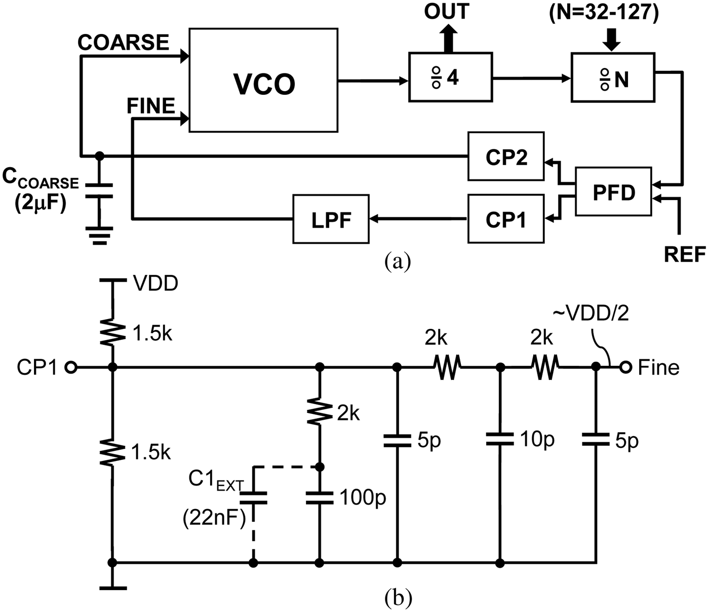
Figure 5 shows the schematic of a 30 GHz integer-N PLL with 5 GHz tuning range designed in a 130 nm SiGe BiCMOS technology [Reference Ruecker22]. The PLL uses a slow coarse tuning loop and a fast fine tuning loop, see also [Reference Hu, Osmany, Scheytt and Herzel18]. Any noise on the fine tuning VCO input has a small effect on the VCO output frequency due to the small tuning gain. By contrast, the coarse tuning input is highly sensitive to any noise due to the high VCO gain, but it is loaded only with a metal-insulator-metal (MIM) capacitor to chip ground in parallel to an external
 $2{\kern 1pt} \;{\rm \mu F}$
capacitor to board ground. The resistive voltage divider at the LPF input keeps the VCO fine tuning voltage, the corresponding VCO gain and the loop bandwidth fairly constant over the PLL tuning range. Figure 6 shows a photograph of the PLL. Due to the large distance between VCO and CMOS blocks (PFD, CP, reference buffer), the substrate noise produced in the CMOS circuitry is strongly attenuated before it reaches the VCO. The VCO is biased from left, whereas the other blocks are bias from bottom or top to minimize the mutual inductances between the bondwires. Figure 7 shows the spectrum for an output frequency of 28.8 GHz measured at the 1:4 prescaler output, where the reference frequency is 75 MHz. The reference spurs at ±75 MHz offset are below −73 dBc. At ±150 MHz we observe spurs due to the substrate coupling from the input buffer to the VCO as discussed in Section 2 2.3. Their level is below −62 dBc.
$2{\kern 1pt} \;{\rm \mu F}$
capacitor to board ground. The resistive voltage divider at the LPF input keeps the VCO fine tuning voltage, the corresponding VCO gain and the loop bandwidth fairly constant over the PLL tuning range. Figure 6 shows a photograph of the PLL. Due to the large distance between VCO and CMOS blocks (PFD, CP, reference buffer), the substrate noise produced in the CMOS circuitry is strongly attenuated before it reaches the VCO. The VCO is biased from left, whereas the other blocks are bias from bottom or top to minimize the mutual inductances between the bondwires. Figure 7 shows the spectrum for an output frequency of 28.8 GHz measured at the 1:4 prescaler output, where the reference frequency is 75 MHz. The reference spurs at ±75 MHz offset are below −73 dBc. At ±150 MHz we observe spurs due to the substrate coupling from the input buffer to the VCO as discussed in Section 2 2.3. Their level is below −62 dBc.

Fig. 5. Schematic of (a) programmable integer-N PLL using two parallel charge pumps for VCO control and (b) the LPF used in this PLL.

Fig. 6. Chip photograph of integer-N PLL.
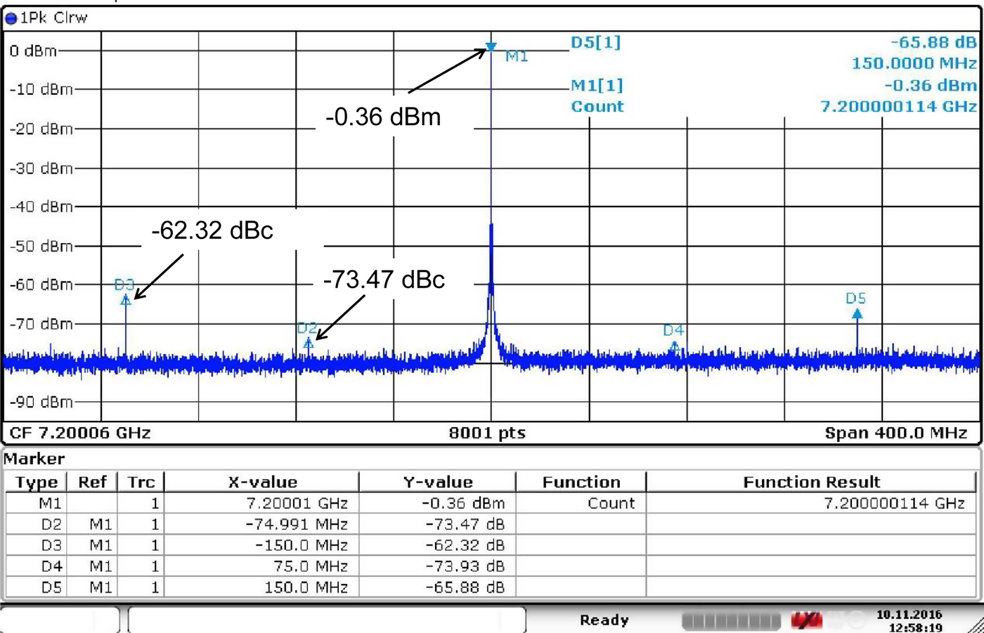
Fig. 7. Measured output spectrum of 28.8 GHz PLL at 1:4 prescaler output.
Near-integer boundary spurs are observed in fractional-N PLLs. Their name is due to the fact that they occur if the total division ratio M N is close to an integer number. In this case, the spurs are located at frequency offsets below the loop bandwidth, where they are hardly filtered by the PLL. Figure 8 shows the spectrum of a 21.2 GHz fractional-N PLL measured at the 1:8 divider output [Reference Osmany, Herzel and Scheytt4]. Here, the reference frequency was 80 MHz, and the division ratios were M = 4 and N = 66.25015. According to (2) in [Reference Osmany, Herzel and Scheytt4] we expect the largest modulation spurs at a frequency offset of
 $ \pm (4 \times 0.25015 - 1) \times 80{\kern 1pt} \;{\rm MHz} = \pm \;48\;{\kern 1pt} {\rm kHz}$
. This is exactly the measured position as evident from Fig. 8. The power level of this spur is as low as −61 dBc due to a careful layout. The measurement showed that the power of this spur is independent of the PD nonlinearity, but responds to changes in the VCO output power. This verifies that the coupling from the VCO output to the PD input is the cause for this spur.
$ \pm (4 \times 0.25015 - 1) \times 80{\kern 1pt} \;{\rm MHz} = \pm \;48\;{\kern 1pt} {\rm kHz}$
. This is exactly the measured position as evident from Fig. 8. The power level of this spur is as low as −61 dBc due to a careful layout. The measurement showed that the power of this spur is independent of the PD nonlinearity, but responds to changes in the VCO output power. This verifies that the coupling from the VCO output to the PD input is the cause for this spur.

Fig. 8. Measured output spectrum of a 21.2 GHz fractional-N PLL at 1:8 divider output [Reference Osmany, Herzel and Scheytt4].
IV. CONCLUSION
We have discussed various mechanisms affecting the spectral purity of phase-locked loops. Emphasis was placed on fractional-N PLLs, where the VCO frequency and the reference frequency are not harmonically related. The effect of quantization noise folding in the nonlinear PD was described and methods for minimizing this effect were proposed. They include a DC offset current at the CP output for linearizing the phase detector, the use of single-loop DSMs and the maximization of the programmable divider speed. It was outlined how the high-frequency VCO output signal can affect the spectral purity of the PLL through substrate coupling and electromagnetic coupling between the bondwires. Remedies were presented to minimize these effects by a proper layout.
ACKNOWLEDGEMENTS
This work was supported by the German Federal Ministry of Education and Research within the research project fast-spot (project number 03ZZ0512A).
 Frank Herzel received his M.S. degree in Physics from the Humboldt University Berlin in 1989, and his Ph.D. degree from the University of Rostock in 1993 in theoretical semiconductor physics. Since 1993, he has been with the IHP, Frankfurt (Oder), Germany, where he was involved in semiconductor device modeling until 1996. Since then, he has been working on the design of silicon ICs for RF communications. His main research interests are design and optimization of high-performance frequency synthesizers for space applications and radar sensors.
 Dietmar Kissinger received the Dipl.-Ing., Dr.-Ing. and habil. degree in Electrical Engineering all from the FAU Erlangen-Nürnberg, Germany, in 2007, 2011 and 2014, respectively. From 2007 to 2010, he was with Danube Integrated Circuit Engineering, Linz, Austria, where he worked as a System and Application Engineer in the Automotive Radar Group. From 2010 to 2014, he held a position as Lecturer and Head of the Radio Frequency Integrated Sensors Group at the Institute for Electronics Engineering, Erlangen. Since 2015, he is a Full Professor at the Technische Universität Berlin and Head of the Circuit Design Department at IHP, Frankfurt (Oder). He is a co-director of the Joint Lab for Radio Frequency Integrated Systems, FAU Erlangen-Nürnberg. His research interests include silicon high-frequency and high-speed as well as low-power integrated systems for communication and automotive, industrial, security and biomedical sensing applications. He has authored or co-authored more than 180 technical papers and holds several patents.