I. INTRODUCTION
Current wireless communication and broadcast standards such as Long Term Evolution (LTE) or Digital Video Broadcasting – Terrestrial (DVB-T) allow the operation in a wide frequency range with a demand for a high linearity power amplifier (PA). In addition, those standards require a certain output power of the transmitter. Since the breakdown voltage of the transistors is continuously decreasing due to further scaling of the technology, the load at the transistor of the PA must be very low-ohmic to still achieve the required output power. Thus the design of the impedance transformation network gets more challenging. Especially, bandwidth and impedance transformation ratio are contradictory.
To circumvent this problem, transformers and dual-band impedance transformation networks can be used. The usage of transformers is very promising [Reference Haldi, Chowdhury, Reynaert, Liu and Niknejad1], but they can hardly be efficiently integrated for circuits in the sub- and low GHz range. Dual-band impedance transformation networks have been investigated mainly for low-noise amplifiers (LNA) [Reference Martins, Fernandes and Silva2]. For PAs, the published approaches use either separated signal paths [3, Reference Bischof4] or are based on discrete passives [Reference Uchida, Takayama, Fujita and Maenaka5]. Dual-band impedance transformation networks are seldom applied for fully integrated PAs since they usually require more bulky inductors [Reference Ghajar and Boumaiza6] which increases chip size and which makes them usually less efficient than an impedance transformation network for a single frequency.
We will show that already the common impedance transformation networks for PAs have the ability for dual-band operation. Hence, we propose a very flexible design procedure that can also take imperfections like losses into account. Based on that, the two most common networks are discussed. Finally, the theory is validated by measurement results of an integrated PA for DVB-T, which can cover more than the UHF IV and V band.
II. DESIGN
A) Architecture
For PAs, LCL, or LLC impedance transformation networks like shown in Fig. 1 are usually used. In this regard, the bias inductor L B is often considered as an unavoidable element for biasing since it does not directly contribute to the impedance transformation. Its inductance is often designed such that it compensates the parasitic capacitance C T of the transistor.
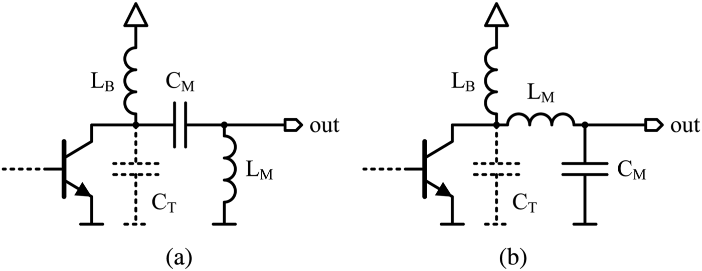
Fig. 1. LCL and LLC impedance transformation networks of typical PAs. (a) LCL, (b) LLC.
In contrast to this, we propose to design the inductance L B and the capacitance C T to achieve the desired impedance transformation at two frequencies. Therefore, no additional inductor is required and the operating band is enlarged. The symbols introduced in Fig. 2 are used for further calculations.
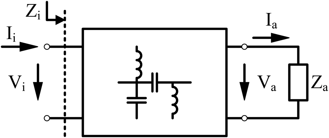
Fig. 2. Definition of the symbols.
B) Design of the network
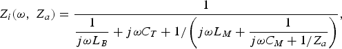
To achieve the maximum uncompressed output power, the load at the intrinsic transistor has to be resistive and has to fit to the operating point [Reference Cripps7]. For the classical design approach, this is only ensured for a single frequency. But the applied networks have the ability to implement the required load impedance for two frequencies. Therefore, the input impedance of the transformation networks is considered. For the LCL network it is given by
 $$Z_i \lpar \omega\comma \; Z_a \rpar =\displaystyle{1 \over {\displaystyle{1 \over {j\omega L_B }}+j\omega C_T+1/\left({\displaystyle{1 \over {j\omega C_M }}+\displaystyle{1 \over {1/\lpar \,j\omega L_M \rpar +1/Z_a }}} \right)}}$$
and for the LLC network by
 $$Z_i \lpar \omega\comma \; Z_a \rpar =\displaystyle{1 \over {\displaystyle{1 \over {j\omega L_B }}+j\omega C_T+1/\left({j\omega L_M+\displaystyle{1 \over {j\omega C_M+1/Z_a }}} \right)}}\comma \; $$
where Z a is the load connected to the transformation network, which is typically 50 Ω.
To achieve dual-band operation, the input impedance of the transformation network has to reveal a certain value for each of the two frequencies. Hence the problem is given by
 $$Z_i \lpar 2{\rm \pi }\, f_1\comma \; Z_{a1} \rpar \mathop=\limits^! Z_{i1} \; {\rm and}\; Z_i \lpar 2{\rm \pi }\, f_2\comma \; Z_{a2} \rpar \mathop=\limits^! Z_{i2}\comma \;$$
where the impedances Z i1 and Z i2 are the required load impedances of the transistor and Z a1 and Z a2 are the externally connected load impedances for the two frequencies of interest, f 1 and f 2. Considering the real and the imaginary parts, those definitions give four equations that are sufficient to solve the problem for the four real parameters L B, C T, C M, and L M.
Unfortunately, the problem is nonlinear, but a numerical solution can be found by appropriate mathematical tools. Therefore, it is beneficial to normalize the problem with respect to frequency and impedance level. We normalized the frequencies by
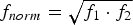 $$f_{norm}=\sqrt {f_1 \cdot f_2 } $$
and the impedances by
 $$R_{norm}=\root 4 \of {\vert Z_{i1} \vert \cdot \vert Z_{i2} \vert \cdot \vert Z_{a1} \vert \cdot \vert Z_{a2} \vert } $$
to achieve a good accuracy of the solution.
For example, the parameters of a lossless LCL network that yields an impedance transformation from 50 to 13 Ω at 600 and 700 MHz are
 $$\matrix{ {L_B=1.75 \, {\rm nH\comma \; }} & {C_T=29.6 \, {\rm pF\comma \; }} \cr {C_M=10.4\, {\rm pF\comma \; }} & {L_M=6.74 \, {\rm nH}.} \cr }$$
Unfortunately, the quality factor of integrated inductors at those frequencies is just in a range of 8–10. For single-frequency impedance transformation networks the impact of the equivalent series resistances R B and R M is small but for the dual-band approach they should be considered. The problem is not getting more complicated by introducing series resistors into Eq. (1). Thus the values of the given example change to
 $$\matrix{ {L_B=2.42\, {\rm nH\comma \; }} & {R_B=1.3 \, \Omega\comma \; } & {C_T=19.6 \, {\rm pF\comma \; }} \cr {C_M=10.2 \, {\rm pF\comma \; }} & {L_M=7.16\, {\rm nH\comma \; }} & {R_M=2.9 \;\Omega } \cr }$$
assuming a quality factor of 8 and 10 at the frequency f 2 for L B and L M, respectively.
Finally, the calculated parameters of the impedance transformation network implement the required impedances at two frequencies. The effect on the compression of the PA around these frequencies and the efficiency of the impedance transformation will be investigated in the following section.
C) Analysis of the compression
One of the main ideas of the load line theory [Reference Cripps7] is to design the load such that the current compression and the voltage compression happen at the same level of excitation. Current compression happens when the transistor switches off. The voltage compression is introduced by bringing the bipolar or the MOS transistor into saturation or into the triode region, respectively. Assuming linear operation up to one or the other compression effect, the maximum uncompressed output power can be calculated as a function of the load impedance and the operating point.
The transfer function from the voltage at input to the voltage at the output of the impedance transformation network is required for this calculation and is for the LCL network
 $$v_{ai}=\displaystyle{{V_a } \over {V_i }}=\displaystyle{{j\omega C_M } \over {j\omega C_M+1/Z_a+1/\lpar j\omega L_M \rpar }}$$
and for the LLC network
 $$v_{ai}=\displaystyle{{V_a } \over {V_i }}=\displaystyle{1 \over {1+j\omega L_M \lpar \,j\omega C_M+1/Z_a \rpar }}.$$
The maximum voltage amplitude  $\hat V_{i\comma max} $ at the transistor is
 $$\hat V_{i\comma max}=V_{DC} - V_{sat}$$
with the supply voltage V DC and the saturation voltage V sat. For class A amplifiers, the maximum current amplitude  $\hat I_{i\comma max} $ is given by the operating point current I C,OP of the transistor and is
 $$\hat I_{i\comma max}=I_{C\comma OP}.$$
Now, the maximum uncompressed output power can be calculated for voltage and for current compression, which is
 $$P_{a\comma V}=\displaystyle{1 \over 2}\vert v_{ai} \lpar \omega \rpar \cdot \hat V_{i\comma max} \vert ^2 \cdot \Re \lpar 1/Z_a \rpar \quad {\rm and}$$
 $$P_{a\comma C}=\displaystyle{1 \over 2}\vert v_{ai} \lpar \omega \rpar \cdot Z_i \lpar \omega \rpar \cdot \hat I_{i\comma max} \vert ^2 \cdot \Re \lpar 1/Z_a \rpar.$$
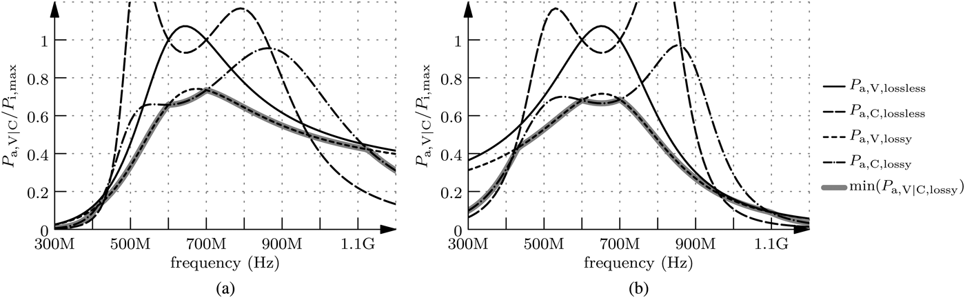
The achieved output power is the minimum of those two. The curves of the two output powers for the lossless and the lossy case are illustrated in Fig. 3, where the powers are normalized to the maximum uncompressed power the transistor can deliver, which is
 $$P_{i\comma max}=\displaystyle{1 \over 2}\hat V_{i\comma max} \cdot \hat I_{i\comma max}.$$
Fig. 3. Curves of the calculated output power for LCL and LLC networks for the cases of voltage and current compression for a lossless and a lossy impedance transformation network; the achieved output power is the minimum of the corresponding curves shown as bold gray line for the lossy case. (a) LCL, (b) LLC.
The two curves for either the lossless or the lossy case intersect at the frequencies, at which the load is designed to fit to the operating point. These are the points of maximum uncompressed output power of the transistor. The degradation of the efficiency at these frequencies is only introduced by the losses of the transformation network. At all other frequencies the efficiency is further reduced by deviations from the optimum load for the transistor.
It can be seen that for the lossless case the curves for the LCL and LLC networks are similar. This is plausible since the LCL network can be transformed to the LLC network by the low-pass high-pass transformation [Reference Vielhauer8]. But for the lossy case, they differ. It is an interesting fact that the efficiency of the impedance transformation network at the designed frequencies is equal for the LLC network but not for the LCL network. However, the maximum efficiency of the LCL network is higher than of the LLC network. In contrast to this, it can be shown that the efficiency of an LLC and an LCL network is equal for the single-frequency approach for equal quality factors of the inductors.
If now the impedance transformation network is considered in combination with the amplifier, it is convenient to describe the amplifier with its Y parameters given by
 $$\left({\matrix{ {I_1 } \cr {I_2 } \cr } } \right)=\left({\matrix{ {I_1 } \cr { - I_i } \cr } } \right)=\left({\matrix{ {Y_{11} \; Y_{12} } \cr {Y_{21} \; Y_{22} } \cr } } \right)\left({\matrix{ {V_1 } \cr {V_2 } \cr } } \right)=Y\left({\matrix{ {V_1 } \cr {V_i } \cr } } \right).$$
Then, the voltage gain from the input of the amplifier to the voltage at the load is
 $$v_{a1} \lpar \omega \rpar =\displaystyle{{V_a } \over {V_1 }}=v_{ai} \lpar \omega \rpar \displaystyle{{ - Y_{21} } \over {1/Z_i+Y_{22} }}.$$
From this, the power at the load can be expressed by
 $$P_a=\vert V_a \vert ^2 \Re \lpar 1/Z_a \rpar =\left\vert {v_{ai} \lpar \omega \rpar \displaystyle{{Y_{21} } \over {1/Z_i+Y_{22} }}V_1 } \right\vert ^2 \Re \lpar 1/Z_a \rpar .$$
For the assumption that the voltage gain from the generator's open circuit voltage V 0 to the voltage V 1 is frequency independent, e.g. by a broadband active driver, the transducer gain G T is proportional to
 $$G_T \propto \left\vert {v\lpar \omega \rpar \displaystyle{{Y_{21} } \over {1/Z_i+Y_{22} }}} \right\vert \Re \lpar 1/Z_a \rpar .$$
If Y 22 is negligible and if Y 21 is constant and taking Eq. (13) into account, it reveals that
 $$G_T \propto P_{a\comma C} .$$
Under all these conditions, the transducer gain can be used for verification.
Although the given relation exists, we like to point out that this is only valid for all given assumptions and that this just describes one of the two effects leading to compression. Hence, proving the bandwidth of PAs only by measuring the small-signal transducer gain is not possible.
The whole design approach is neither limited to PA applications nor to the discussed topologies. It can be easily extended to other structures that are more suited for dual-band operation and it can also include transmission lines. For PA applications, alternative networks require more inductors, which increase chip size and which are therefore not beneficial. However, since the transformation network relies on C T as a parameter of the transistor, it has to be pointed out that in case of C T being too small to allow the desired transformation at two frequencies, other options can be considered such as changing the size or layout of the transistor array, using another arrangement of L M and C M or changing the transformation frequencies.
III. VERIFICATION
A) Description of the integrated circuit
A chip using an LCL network designed with the described approach was implemented in IHP's 250 nm SiGe BiCMOS technology. The schematic representation of the PA is shown in Fig. 4. It consists of a common-collector driver stage and the cascode power stage with the described dual-band output network. Furthermore, biasing networks are shown for the driver and the power stage using a replica-biasing scheme to set the current in the driver and output stage. A micrograph of the chip is presented in Fig. 5. The chip size is 1.3 mm × 1.2 mm. The implemented circuit is differential and uses a cascode for the main stage. Since the cascode output node is highly decoupled from the input node, resulting in a very small S 12 of the stage, the Rollet's factor and therefore stability is improved. The capacitance C T is formed only by the parasitic capacitances of the transistor field. To achieve the maximum bandwidth, an active driver in combination with a resistive input matching is applied.
Fig. 4. Schematic representation of the whole differential power amplifier and bias circuits.
Fig. 5. Chip micrograph, size 1.3 × 1.2 mm2.
Furthermore, a passive network between the driver and the main stage has been introduced. Since the exponential characteristic of the bipolar transistors leads to an expansion of their collector currents, the average collector current with excitation is higher than the operating point current. For a well-defined limitation of this effect, while the collector current expands the gain has to remain constant. The task of the network consisting of R 4 and R 5 is to limit the expansion of the average collector current of the main stage, since the base current flowing through the resistors tends to expand in the same way and works against the effect. Therefore the gain is more flat and the linearity is increased.
B) Measurement results
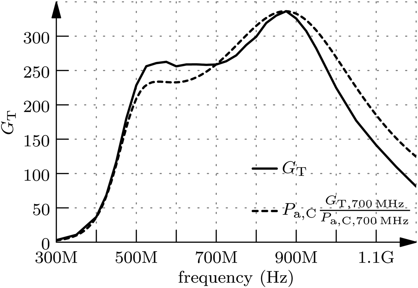
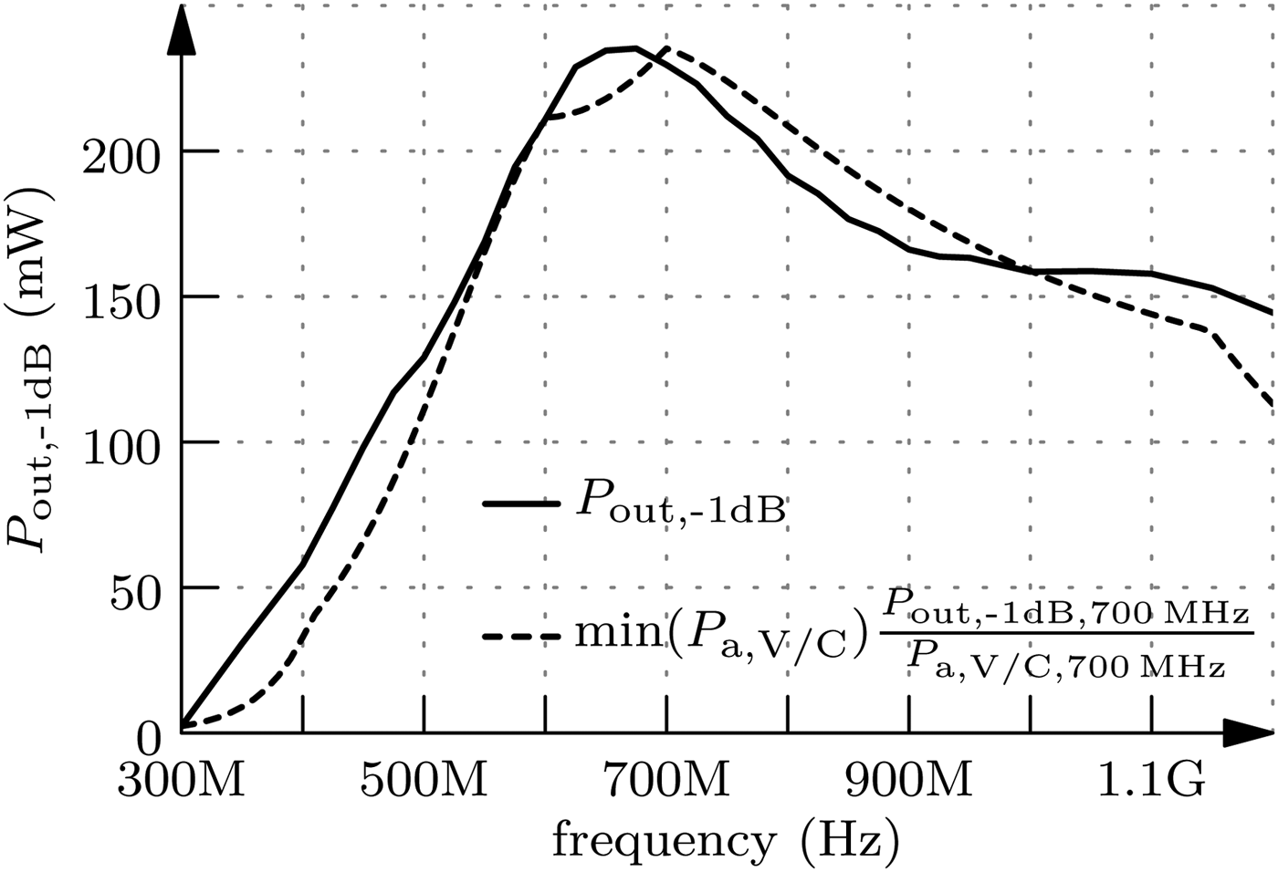
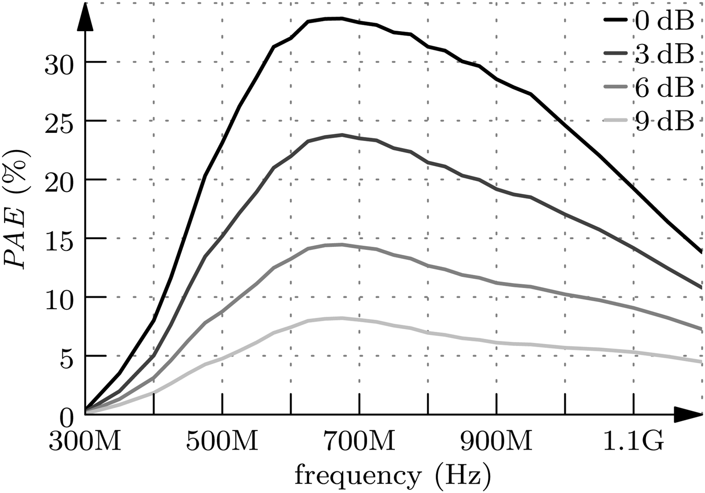
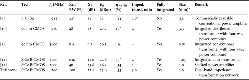
The circuit was measured on-wafer. Compression measurements were performed by a Rhode & Schwarz network analyzer ZVA 67. The transducer gain G T is shown in Fig. 6. For comparison the transducer gain is plotted in linear scale and P a,C is scaled to the value of G T at the frequency f 2. Thus, it can be seen that its shape fits well to P a,C in Fig. 3. Deviations for higher frequencies can be explained by impacts from the driver circuit. The compression point measurements were performed in steps of 50 MHz. The output power at the 1 dB compression point is depicted in Fig. 7. Again, a linear scale is chosen to be able to compare the trace with Fig. 3. Although its shape differs slightly from the prediction, it can be seen that a linear model can be used to estimate the linear uncompressed output power. The measured 3 dB large-signal bandwidth is more than 700 MHz around the center frequency of 700 MHz leading to a relative bandwidth of more than 100 %. Finally, the power added efficiency PAE at the 1 dB compression point as a function of the frequency is shown in Fig. 8. Also thereby, the large bandwidth is proven. In addition, the values are also given for 3, 6, and 9 dB back-off. Table 1 compares the designed power amplifier with dual-band impedance transformation network to other state-of-the-art wideband power amplifiers. The presented chip reaches the highest relative bandwidth in comparison.
Fig. 6. Measured and calculated transducer gain versus frequency.
Fig. 7. Measured and calculated output power at the 1 dB compression point versus frequency.
Fig. 8. Measured power added efficiency versus frequency for 0–9 dB back-off.
Table 1. State-of-the-art wideband power amplifiers.
*Estimated.
†Determined as saturated output power instead of output power at 1 dB compression point.
IV. CONCLUSION
It was shown that the common impedance transformation networks for PAs have the ability to implement the required impedance transformation for two frequencies without additional inductors. This increases the frequency range of operation. The dimensioning of the circuit can be done by numerically solving the nonlinear system of equations. Also, imperfections like losses can be considered leading to a fast design process. Based on this, the maximum uncompressed output power of a PA can be estimated. The theory is validated by implementing and measuring an integrated PA.
ACKNOWLEDGEMENTS
This work was partly funded by the Federal Ministry of Education and Research (BMBF) in the excellence cluster CoolSilicon, project CoolBroadcastRepeater, and by the European Community's Seventh Framework Programme (FP7/2007–2013) under grant agreement no. 242411 (E-SPONDER).
Robert Wolf was born in Karl-Marx-Stadt, Germany, in 1984. He received the Dipl.-Ing. degree in Electrical Engineering from the Technische Universität Dresden, Dresden, Germany, in 2009, where he is currently working toward the Ph.D. degree. Since 2010, he has been the Group Leader of the Smart Power Amplifier Group, Chair for Circuit Design and Network Theory, Technische Universität Dresden, Dresden, Germany. His main research interests include system analysis and the design of integrated control systems for efficiency enhancement of RF power amplifiers.
Niko Joram was born in Oelsnitz, Germany, in 1984. He received his M.Sc. degree in Information Systems Engineering from the Technische Universität Dresden in 2009, where he is currently working toward the Ph.D. degree. Since 2013, he has been the Research Group Leader of the Local Positioning Design Group at the Chair for Circuit Design and Network Theory, Technische Universität Dresden. His main research interests include circuit and system design for robust localization systems.
Stefan Schumann studied Electrical Engineering at the Dresden University of Technology, Dresden, Germany, and the Delft University of Technology, Delft, The Netherlands. He received the Dipl.-Ing. degree in 2006 and the Ph.D. degree in 2012, both from the Dresden University of Technology, Dresden, Germany. His main research interest is the design and measurement theory of integrated circuits for wireless applications. He is with the Chair for Circuit Design and Network Theory at the Dresden University of Technology, Dresden, Germany. Mr. Schumann was the recipient of the 2006 AMD Award for an excellent diploma thesis in the field of microelectronics.
Frank Ellinger was born in Friedrichshafen, Germany, in 1972. He received the Diploma degree in Electrical Engineering from the University of Ulm, Germany, in 1996, the M.B.A. degree, Ph.D. degree in Electrical Engineering, and the Habilitation degree in high-frequency circuit design from ETH Zürich, Switzerland, in 2001 and 2004, respectively. Since August 2006, he has been a Full Professor and the Head of the Chair for Circuit Design and Network Theory, Technische Universität Dresden, Germany. From 2001 to 2006, he was the Head of the RFIC Design Group, Electronics Laboratory, ETH Zürich (ETHZ), Zürich, Switzerland, and a Project Leader of the IBM/ETHZ Competence Center for Advanced Silicon Electronics hosted at IBM Research, Rüschlikon, Switzerland. He authored or coauthored more than 300 refereed scientific papers.