I. INTRODUCTION
A microstrip antenna is the most useful low-profile antenna due to its light weight, small size, and low cost. The conventional circular microstrip patch antenna (CMPA) is very easy to fabricate and assemble [Reference Kumar and Ray1], and hence it has become an attractive radiator for modern wireless and microwave communication systems. The conventional CMPA, resonating at its fundamental TM11 mode, produces linearly polarized field along its broadside. The plane of polarization is determined by the vertical xz-plane as indicated in Fig. 1. This x–z plane is referred as E plane. However, some extent of orthogonally polarized field (orthogonal to xz-plane or E p-lane) is always evident [Reference Huynh, Lee and Lee2, Reference Lee, Luk and Tam3] which is referred to as cross-polarized (XP) radiation. The XP radiation fields are more significant in the H-plane (yz-plane) than in the E-plane as obtained in open literature [Reference Garg, Bhartia, Bahl and Ittipiboon4]. In particular, the angular region, where the cross-polarization levels go 20 dB lower than the co-polarization levels, are only few degrees near the broadside direction in the H-plane. This evidently is a hindrance to the applications, such as adaptive antenna arrays for cellular, mobile land, or other wireless communications, where wide coverage is usually required as indicated in [Reference Chen and Michael5]. Consequently, scientist and researchers have been addressing this issue of lowering XP radiation, particularly in H-plane since past two decades. Experimental studies indicate the considerable XP level in the H-plane, which typically appears about 15 dB below the peak gain.

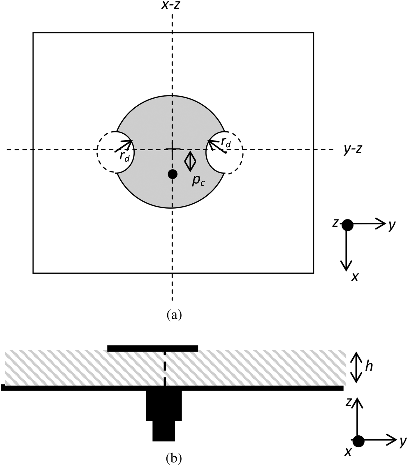
Fig. 1. Schematic representation of the proposed circular microstrip antenna with the circular cut defected surface. (a) Top view and (b) Side view.
Few handful investigations, by modifying the feed structure of patch antenna, were reported in [Reference Petosa, Ittipiboon and Gagnon6–Reference Chen and Chia9] for reduction of XP radiation. Dual-feed structures with 180° phase difference have been employed in [Reference Petosa, Ittipiboon and Gagnon6, Reference Schejbal and Kovarik7]; whereas meander line feeding mechanism is utilized in [Reference Li, Lai, Luk and Lau8]. About 20 dB of XP suppression has been reported in [Reference Li, Lai, Luk and Lau8]. Use of probe-fed half-wavelength strip is reported in [Reference Chen and Chia9] to improve co-cross polarization ratio and 20 dB of XP suppression compared with co-polarized peak gain is evident from the literature. The modification done to the ground plane shape to suppress the XP radiation about 10–15 dB, is apparent in [Reference Wong, Tang and Chiou10, Reference Hsu and Wong11].
Recently, there has been an increasing interest in using defected ground structures (DGS) in microwave and millimeter wave applications. Guha et al. [Reference Guha, Biswas and Antar12] were the first to propose the concept of DGS for minimizing XP radiation for a microstrip patch antenna. Subsequent investigations [Reference Kumar and Guha13–Reference Kumar and Guha16] confirm that the H-plane XP radiation can be minimized by dot, arc and ring shaped DGS. A recently reported article [Reference Kumar and Guha17] has shown about 10–12 dB suppression of H-plane XP radiation compared with conventional circular microstrip antenna using arc-shaped DGS. However, all these investigations lead to complexity in manufacturing process and moreover, authors feel that more investigations are required to find a more simple technique for suppression of the XP radiation.
With this in view, a new and simplified patch structure has been investigated in the present paper and about 27–28 dB of XP suppression compared with co-polarized peak gain is revealed. The newly proposed patch structure is basically a circular patch with circular cut defects placed symmetrically at its H-plane as shown in Fig. 1. The source of XP fields was theoretically analyzed in [Reference Lee, Luk and Tam3] and the first higher-order mode was attributed to this phenomenon. Indeed the conjecture of automatic generation of TM21 mode (the first higher-order mode for circular patch) leads to conceive such structure, which will affect the field distribution of TM21 mode, whereas that for TM11 dominant mode is kept unaltered. In order to alleviate the lacunae of earlier studies, the present paper gives a clear insight in to the source of XP radiation. The minimization of XP radiation relative to co-polarized peak gain with the proposed structure is pictorially documented. Few representative measured results are also incorporated to validate the proposed idea.
The present structure may be utilized to the wireless systems where better XP performance is the major issue, e.g. wireless base station network, good quality EMI sensors, linearly polarized array, etc.
II. BACKGROUND, PARAMETRIC STUDIES, AND PROPOSED STRUCTURE
A) Background
The conventional CMPA, resonating at its fundamental TM11 mode, produces broadside radiation where the electric fields are linearly polarized along the E-plane (x–z). The radiations are inherently from the fringing fields situated at radiating edges as we know from open literature [Reference Garg, Bhartia, Bahl and Ittipiboon4]. However, few fringing fields of the dominant mode are existing in regions A and B as indicated in Fig. 2. It, in fact, takes part in radiation and may produce appreciable amount of power at a certain angle, which may be attributed for XP radiation. The dotted line in Fig. 2(a) shows the electric surface current along the direction, orthogonal to the E-plane; whereas the solid line indicates the same for the pure TM11 mode. The first component of electric surface current is accountable for XP radiation. This sort of orthogonal component of dominant mode for XP radiation is apparent from [Reference Kumar and Guha17]. It is basically due to orthogonal resonance of week TM11 mode as reported. Along with this, the automatic excitation of orthogonal higher-order mode TM21 is the key factor in producing high XP radiation from the CMPA. The field and current distributions are shown in Fig. 2 for the TM11 and TM21 modes.
Fig. 2. Electric field and current distribution over patch surface (a) for the dominant TM11 mode and (b) for the next higher-order TM21 mode.
It is clear from Fig. 2(b) that the resonance for the TM21 mode is orthogonal to the E-plane and hence produces high XP fields. This is also evident from [Reference Lee, Luk and Tam3]. A close inspection of Fig. 2 discloses that the radiations mainly from regions A and B are responsible for XP radiation. Hence a pair of circular cut defect has been organized symmetrically at the H-plane as shown in Fig. 1, which can eliminate the prospect of survival of E-fields on those A and B regions. As a consequence the proposed circular cut-defected circular patch antenna (CCDCPA) can minimize the orthogonal resonance as well as produce better XP performance.
B) Parametric studies
The parametric studies, using commercially available software package (high-frequency structure simulator; HFSS v. 14), is utilized to investigate the radiation characteristics of the proposed structure. This is crucial to optimize the dimension of the defect on patch surface.
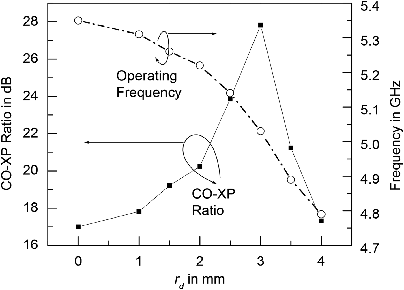
Figure 3 shows the simulated radiation characteristics of the proposed CCDCPA with the defects of different radial dimensions r d. The radiation characteristics of simple CMPA with r d = 0 is also incorporated in the same plot for comparison. It appears that if the radius of the defect r d is increased up to 3 mm, the XP radiation compared to peak co-polarized gain in the H-plane decreases in the present structure. Gradually as r d is increased above 3 mm, the XP radiation performance degrades more compared with maximum co-polarized gain. About 10–11 dB improvement in XP radiation compared with that from CMPA, is revealed with proposed CCDCPA (r d = 3 mm). Consequently about 27–28 dB of XP suppression compared with maximum co-polarized gain is achieved. It is also apparent from Fig. 3(a) that XP performance degrades in the E-plane due to incorporation of defect on the patch surface. But in the present investigation it is still below 40 dB compared with maximum co-polarized gain. This may be tolerable for any wireless communication link. The profile of co-polarization to cross polarization radiation ratio (Co–XP ratio) as a function of radius of the defect is presented in Fig. 4. It reveals that the best XP radiation isolation compared with its peak co-polarized gain is achieved with r d = 3 mm and is therefore chosen for investigation.
Fig. 3. Comparison of the radiation pattern of the proposed CCDCPA with variable r d and the conventional CMPA. (a) The E-plane and (b) the H-plane.
Fig. 4. Variation of the CO–XP ratio and the operating frequency of the proposed structure with variable radius of the defect on the patch surface.
C) Proposed structure
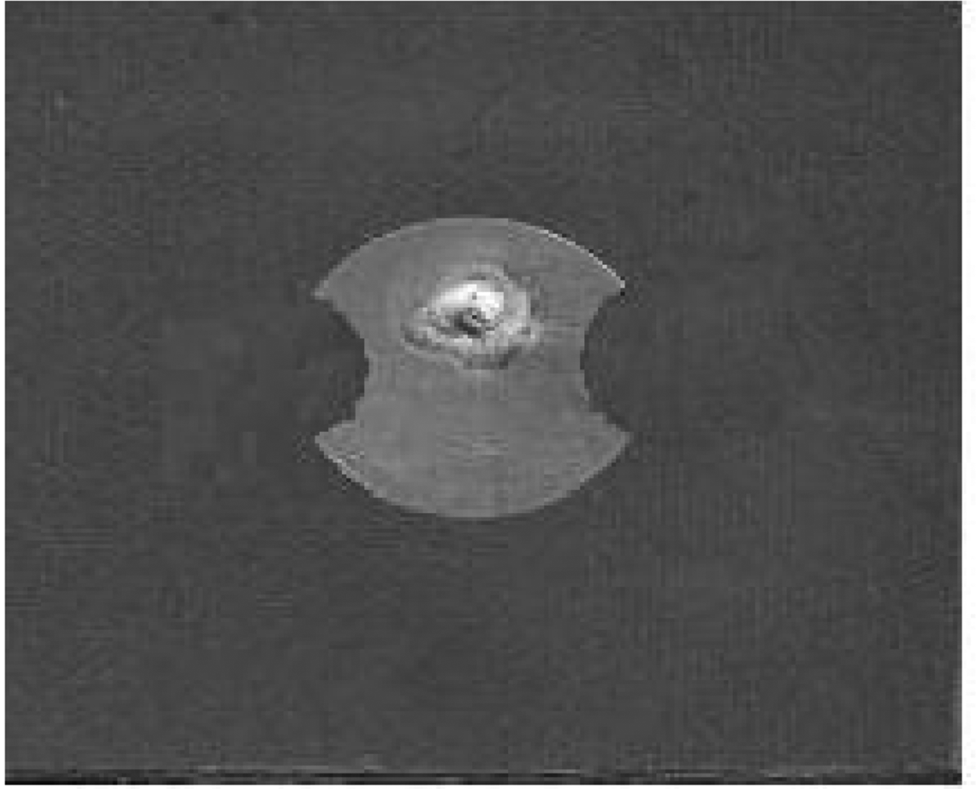
A pair of circular cut defect in CMPA gives birth to the proposed structure as shown in Fig. 1 of CCDCPA. RT duroid (ε r = 2.33) of 1.58 mm thickness has been utilized as the substrate over the ground plane of 90 × 90 mm. The patch of radius a = 10 mm is designed to operate about 5 GHz. Two circular sections each of radius r d = 3 mm have been removed symmetrically to form a CCDCPA-based on parametric studies. The investigation has been performed using [18] to obtain better matching and good Co–XP ratio. The feed position has been shifted to 2.8 mm from the center of the patch for optimization. A prototype has also been fabricated as shown in Fig. 5 with the above-mentioned parameters and is utilized to validate the observed phenomenon.
Fig. 5. Fabricated prototype of the proposed CCDCPA with r d = 3 mm.
III. DISCUSSIONS AND MEASUREMENTS
Simulated and experimental investigations of the input and radiation characteristics with the conventional CMPA and the proposed CCDCPA are documented in the following section. The fabricated CCDCPA shown in Fig. 5 is utilized for measurement purpose. But before discussing the results, let us initially concentrate on the reason behind the observations documented in section II B. The parametric study of the proposed structure reveals that for lower dimension of the defect, CO-XP ratio is not good but as soon as it increases, CO-XP ratio improves and the best result is obtained at r d = 3 mm. In fact, when r d is small, then it cannot perturb or eliminate all electric fields situated in regions A and B of Fig. 2. The fact is clear from the review done on the field components beneath the patch as indicated in the following section. The field components obtained from open literatures as
 $$\left. \matrix{{E_\rho } = {E_\varphi } = {H_z} = 0 \hfill \cr {E_z} = {B_{mnp}}{A_2}{J_m}\left( {{k_\rho }\rho } \right)\cos m\varphi \cos {k_z}z \hfill \cr {H_\rho } = - \displaystyle{1 \over {\mu \rho }}{B_{mnp}}{A_2}{J_m}\left( {{k_\rho }\rho } \right)m\sin m\varphi \cos {k_z}z \hfill \cr {H_\varphi } = - \displaystyle{1 \over \mu }{B_{mnp}}{A_2}{{J}_m}^{\prime}\left( {{k_\rho }\rho } \right)\cos m\varphi \cos {k_z}z \hfill} \right\}$$
For electric surface current J s over the patch surface, we may write
 $$\left({J_s } \right)_E\,=\hat z \times H_\rho\comma$$
along the E-plane or x–z plane
 $$\left({J_s } \right)_H\,=\hat z \times H_\varphi\comma$$
along the H-plane or the y–z plane.
The inspection of equation (1) shows that appreciable amount of electric field resides near the edge in the orthogonal plane (y–z or H-plane). As a result, for small radius of the defect r d; it will not interact much with the H φ-component. Thereby electric surface current along the direction, orthogonal to E-plane is not eliminated fully as is clear from equations (2) and (3). Consequently, an extended circular cut defect with larger r d over a relatively wider area at the patch boundary has been considered and about 27.5 dB of XP suppression compared with peak co-polarized gain in the H-plane is observed for r d = 3 mm. It is also observed that when r d becomes too large, i.e. greater than 3 mm; the radiation from probe is more exposed and contributes in the radiation pattern of CCDCPA resulting higher XP radiation. The XP radiation suppression of about 17 dB compared with peak co-polarized gain in the H-plane is observed for r d = 4 mm, which is similar to simple CMPA.
The variation of the operating frequency as a function of r d of CCDCPA is also shown in Fig. 4. Each resonant frequency value is extracted from the minima of return loss profile, which is well below −30 dB in each case. It is apparent from the figure that as the dimension of the defect r d on the patch surface increases, operating frequency decreases. The incorporation of the defect has led to the slight shift in resonance frequency toward the lower side of the spectrum. It may be due to the slight lengthening of electric surface current path.
Electric field over the patch boundary at the orthogonal plane is presented in Figs. 6(a) and 6(b) for CMPA and proposed CCDCPA, respectively. It is clear from the figure that, near the patch boundary at the orthogonal plane (y–z or H-plane), crowding of the electric field is more in CMPA than the proposed structure. Electric surface current (J s) over the patch surface has been shown in Figs. 6(c) and 6(d) for CMPA and proposed CCDCPA, respectively. It reveals that J s is less prone to flow along the orthogonal direction in the proposed structure compared with simple CMPA. Hence Fig. 6 further corroborates the fact of low XP radiation from the proposed structure compared with CMPA.
Fig. 6. Comparison of the electric field components and the electric surface currents of the conventional CMPA and the proposed CCDCPA. (a) E-fields near the patch boundary on the orthogonal plane of CMPA. (b) E-fields near the patch boundary on the orthogonal plane of the proposed CCDCPA with r d =3 mm (c), J s on the patch surface of CMPA (d). J s on the patch surface of the proposed CCDCPA with r d = 3 mm.
Figure 7 shows the measured reflection coefficient profile as a function of frequency for both the prototypes. Simulation results are also incorporated in the same plot for comparison. Excellent agreement between simulation and measurements is evident. The figure once more substantiates the observation presented in Fig. 4.
Fig. 7. Simulated and measured reflection coefficient profiles of the CMPA and the proposed CCDCPA with r d =3 mm.
Figure 8 shows the comparison of radiation pattern for conventional and proposed structure. Simulation and measured results show close mutual agreement among them. Same type of observation discussed earlier is noted. About 27.5 dB of XP suppression compared with maximum co-polarized gain is revealed while that for conventional structure is about 16 dB. Therefore, the proposed structure present much better Co–XP ratio compared with the conventional CMPA.
Fig. 8. Comparison of the radiation pattern of the proposed CCDCPA with r d =3 mm and the conventional CMPA. (a) The E-plane and (b) the H-plane.
IV. CONCLUSION
A new circular cut defected circular patch antenna is proposed for significant improvement of Co–XP ratio for microstrip patch of circular geometry. About 10–11 dB of XP suppression compared with XP radiation from the conventional circular patch is achieved. This results about 27–28 dB isolation between Co and XP radiations in the H-plane, while that for conventional geometry, it is only 16–17 dB. The proposed geometry is very simple, easy to fabricate and therefore helps in effortlessness manufacturing process. The new antenna is definitely useful for the wireless communication system where polarization diversity is required to establish with such low-profile microstrip radiator.
ACKNOWLEDGEMENT
The authors would like to thank Professor D. Guha and Dr. J. Y. Siddiqui of Institute of Radio Physics and Electronics and A. Ghosh of Department of ECE, Mizoram University for their support by which the whole fact is established in the present form.
Abhijyoti Ghosh is currently working as an Assistant Professor in the Department of Electronics and Communication Engineering, Mizoram University, Tanhril, Aizawl, Mizoram, India. He has done his B.E. in Electronics and Tele-Communication Engineering from North Maharashtra University, Jalgaon, Maharashtra, India in 2005 and M.Tech. in Mobile Communication and Network Technology from West Bengal University of Technology, Kolkata, West Bengal, in 2007. He has more than 7 years of experience in teaching. He has published a number of papers in various journals, conference proceedings. His research interest includes microstrip patch antennas and wireless communication systems.
Sudip Kumar Ghosh is currently working as an Assistant Professor in the Department of Electronics and Communication Engineering, Siliguri Institute of Technology, Sukna, Darjeeling, under West Bengal University of Technology, West Bengal, India. He has received his M.Sc. degree in Electronics from Vidyasagar University in 2005 and M.Tech. degree in Communication and Networking from West Bengal University of Technology in 2007. He has more than 6 years of experience in teaching. He has published a number of papers in various journals and conference proceedings. His research interest includes radiation and broadband properties of microstrip antenna, optoelectronic oscillator, etc.
Dia Ghosh was born in Siliguri, West Bengal, in October 1982. She received her B.Tech. degree from West Bengal University of Technology in 2005 and M.Tech. degree from the University of Burdwan in 2011. She served as maintenance engineer in Zee Akaash News Pvt. Ltd. from 2006 to 2009. At present she is associated with the Siliguri Institute of Technology, Siliguri as an Assistant Professor and also working toward her Ph.D. in the field of Communication Engineering. Her research interest includes microstrip antennas, injection-locked oscillators, optoelectronic oscillators, and microwave devices.
Sudipta Chattopadhyay was born in West Bengal on September 10, 1974. He received his B.Sc. (Physics Honors) from the University of Calcutta in 1996 and B.Tech., M.Tech., and Ph.D. from the Institute of Radio Physics and Electronics, University of Calcutta in 1999, 2001, and 20011, respectively. He is currently working as an Associate Professor of Siliguri Institute of Technology under West Bengal University of Technology, West Bengal, India. He is listed in Marquis Who's Who in the World, USA, 26th Ed, 2009, and also listed in 2000 Outstanding Intellectuals of the 21st Century, UK, 2010. He is a member of IEEE Antennas and Propagation Society and reviewer of several international journals. He has several publications in referred international journals and international conferences in his credit. His area of research includes microwave antennas, microstrip and integrated antennas, and computer-aided design of patch antennas.