I. INTRODUCTION
Rectangular waveguide terminations are widely used in telecommunications and radar systems. For example, front-ends of satellites can integrate between 50 and several hundred terminations. These are usually coupled with circulators in order to prevent microwave sources being detuned by mismatched loads.
These devices are made of a short-circuited waveguide section in which an absorbing material is inserted. Polymer composites or ceramics can be used depending on the power handling capability required. In order to ensure a low Voltage Standing Wave Ratio (VSWR), i.e., a low reflected power, over a wide band of frequencies, these absorbing materials are generally shaped in the form of a pyramid or multistep section. In the case of a polymer composite, a large parallelepiped of absorbing materials is molded and then machined to obtain the desired geometry, which makes devices quite costly. Moreover, the development cycle of new devices (modification of the absorbing material geometry) is time-consuming work.
In this context, three-dimensional (3D)-printing technology appears to be a very exciting alternative for producing low-cost microwave terminations and reduce the development time of these devices. Indeed, Fused Deposition Modeling (FDM) technologies, which consist in depositing a fused polymer layer-by-layer, make it possible to test and very easily build a new geometry without huge additional cost. Moreover, commercial materials compatible with FDM technologies are very low in cost. Several publications demonstrated that this 3D-printing technique can be used to realize microwave devices such as antennas [Reference Liang, Xiaoju, Shemelya, Mac Donald and Hao1–Reference Vera-Lopez, Rojas-Nastrucci, Cordoba-Erazo and Weller3] or transmission lines [Reference Rojas-Nastrucci, Weller, Lopez Aida, Fan and Papapolymerou4]. FDM materials usually have a low dielectric constant together with a moderate loss tangent [Reference Deffenbaugh, Rumpf and Church5, Reference Arbaoui, Laur, Maalouf and Queffelec6]. However, when loaded with carbon particles, thermoplastics show dielectric properties compatible with microwave absorbing applications i.e., high loss tangent [Reference Arbaoui, Laur, Maalouf and Queffelec6]. In a previous study, we thus demonstrated that a carbon-loaded Acrylonitrile Butadiene Styrene (ABS) polymer makes it possible to realize microwave terminations with a VSWR lower than 1.025 over the X-band [Reference Arbaoui7]. However, FDM technology has a limited resolution and the devices contain defects that could limit the reproducibility of the reflection parameter (S 11) and the increase of frequency when the size of defects tends to be of the same order as of the wavelength.
In this paper, our work was focused on the reproducibility issue. We studied the effect of the absorbing material geometry and printing conditions on the S 11 of K-band rectangular waveguide terminations. The first part of this paper discusses the choice of an absorbing material topology suited to 3D-printing manufacture. We then detail the 3D-printing process and the associated parameters that were used to realize the microwave devices. Finally, we present the performance of the 3D-printed microwave terminations. The discussion will particularly concentrate on the influence of printing parameters on S 11 amplitude and reproducibility.
II. APPROPRIATE CHOICE OF ABSORBING MATERIAL GEOMETRY
Classically, rectangular waveguide terminations consist of a short-circuited section of metallic rectangular waveguide loaded with an absorbing material insert. In our case, we used a 10-cm long WR42 waveguide, with lateral dimensions a = 10.67 mm and b = 4.32 mm, for which the monomodal TE10 frequency band is between 18 and 26.5 GHz. The absorbing material was a carbon-loaded ABS polymer. Its dielectric properties were extracted from the K-band with a rectangular waveguide method similar to the one employed in [Reference Arbaoui, Laur, Maalouf and Queffelec6]: ε r = 9.4 and tanδ = 0.27.
To ensure good impedance matching over a wide frequency band, the absorbing material was shaped into the overall form of a pyramid. As illustrated in Fig. 1, this absorbing material can be 3D printed in three different directions: (i) along l, the direction of wave propagation; (ii) along a, the width of the waveguide; or (iii) along b, the height of the waveguide. Such geometry leads to 3D-printing issues: when the pyramid was printed along l, the fused polymer did not have time to harden even if the 3D-printing speed was slow because its tip had a very low surface. When the pyramid was printed along a or b, a support material was required, which induced a very rough surface when it was removed. 3D-printed pyramidal shapes thus have reproducibility issues, and random defects on the surface have to be removed by post-machining.
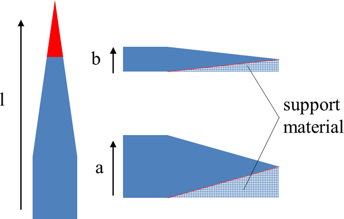
Fig. 1. Illustration of the different 3D-printing configurations for a pyramid-shaped piece of absorbing the material. Red zones are subject to defects or high roughness.
One solution appears to be to remove the tip of the pyramid. We numerically studied the reflection parameter of a pyramid-shaped piece of absorbing material with a truncated tip. The geometry of the absorber is illustrated in Fig. 2, where l b = 10 mm and l p = 40 mm. The effect of the size of the tip (a p and b p) was studied by performing electromagnetic simulations with Ansys HFSS software.
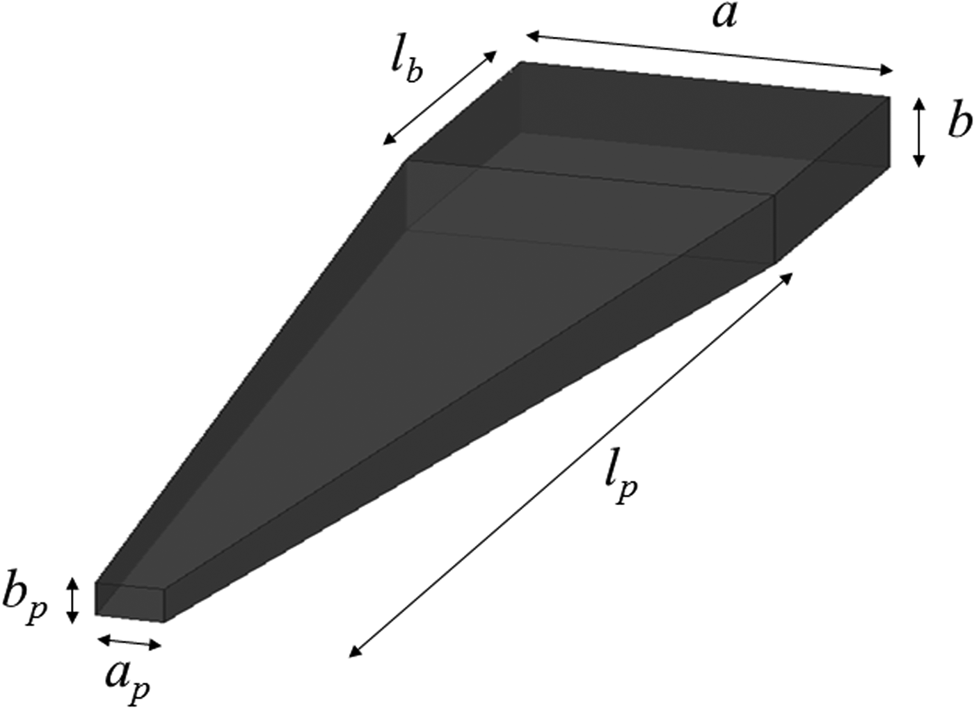
Fig. 2. Illustration of the pyramid-shaped absorbing material with a truncated tip.
Figure 3 presents the simulated S 11 amplitude of the microwave termination loaded with a truncated pyramidal absorber for different lateral dimensions of the tip. The reflection level is below −34 dB over the whole K-band when the dimensions of the tip are 0.5 × 0.5 mm2. This value strongly increases when the surface of the tip increases. Indeed, when tip dimensions are 2 × 2 mm2, the reflection level is only below −17 dB between 18 and 26.5 GHz. This geometry thus appears to be very sensitive to the truncation of the tip due to the position of the tip placed in a maximum electric field of TE 10 mode.

Fig. 3. Amplitude of the reflection level (S 11) of a microwave termination consisting of a short-circuited rectangular waveguide loaded with a truncated pyramid-shaped absorber between 18 and 26.5 GHz for different dimensions of absorber tip.
The Asymmetrical Tapered Wedge (ATW) geometry, presented in Fig. 4, seems to be better suited to 3D-printing technology. Indeed, the tip of the pyramid, which can be subject to random defects, is placed in a minimum electric field.
Fig. 4. Illustration of the ATW-shaped absorbing material with a truncated tip.
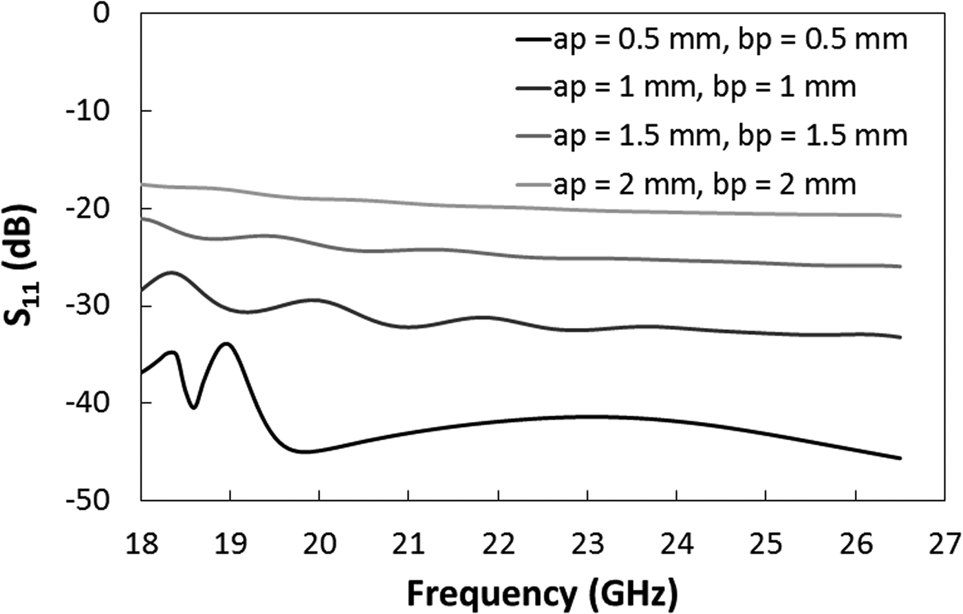
Figure 5 shows the simulated reflection level of microwave terminations made of a short-circuited rectangular waveguide loaded with an ATW-shaped absorber that can have different tip dimensions. The length of the base l b and the one of the ATW pyramid l p are the same as those of the previous structures. The reflection parameter was kept below −30 dB up to a tip as large as 2 × 2 mm2. This geometry thus appeared to be much less sensitive to a truncation of the tip than the previous one.
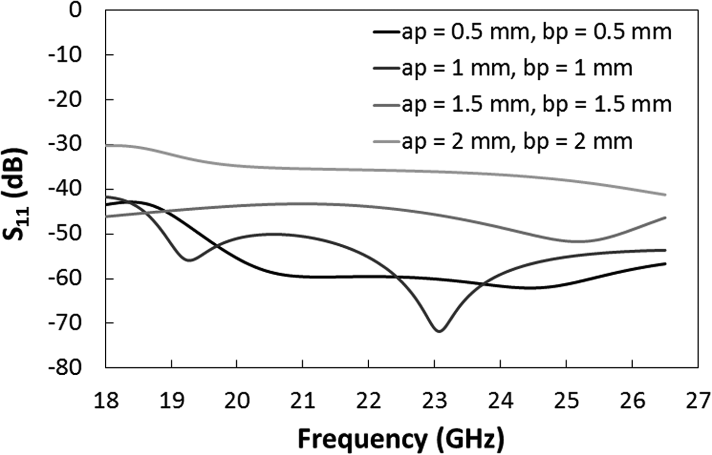
Fig. 5. Amplitude of the reflection level (S 11) of a microwave termination constituted of a short-circuited rectangular waveguide loaded with a truncated ATW-shaped absorber between 18 and 26.5 GHz for different absorber tip dimensions.
One should note that ATW geometry has another main advantage. Unlike a classic pyramid shape, ATW geometry can be 3D printed in the directions l, a or b without requiring support materials.
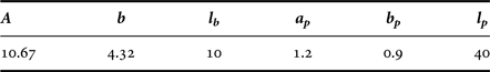
Table 1 gives the dimensions of the ATW geometry finally selected, as these gave the best tradeoff between printability and simulated performance. Figure 6 shows the reflection parameter of this termination as a function of frequency. These dimensions lead to a S 11 parameter of less than −43 dB over the whole X-band.
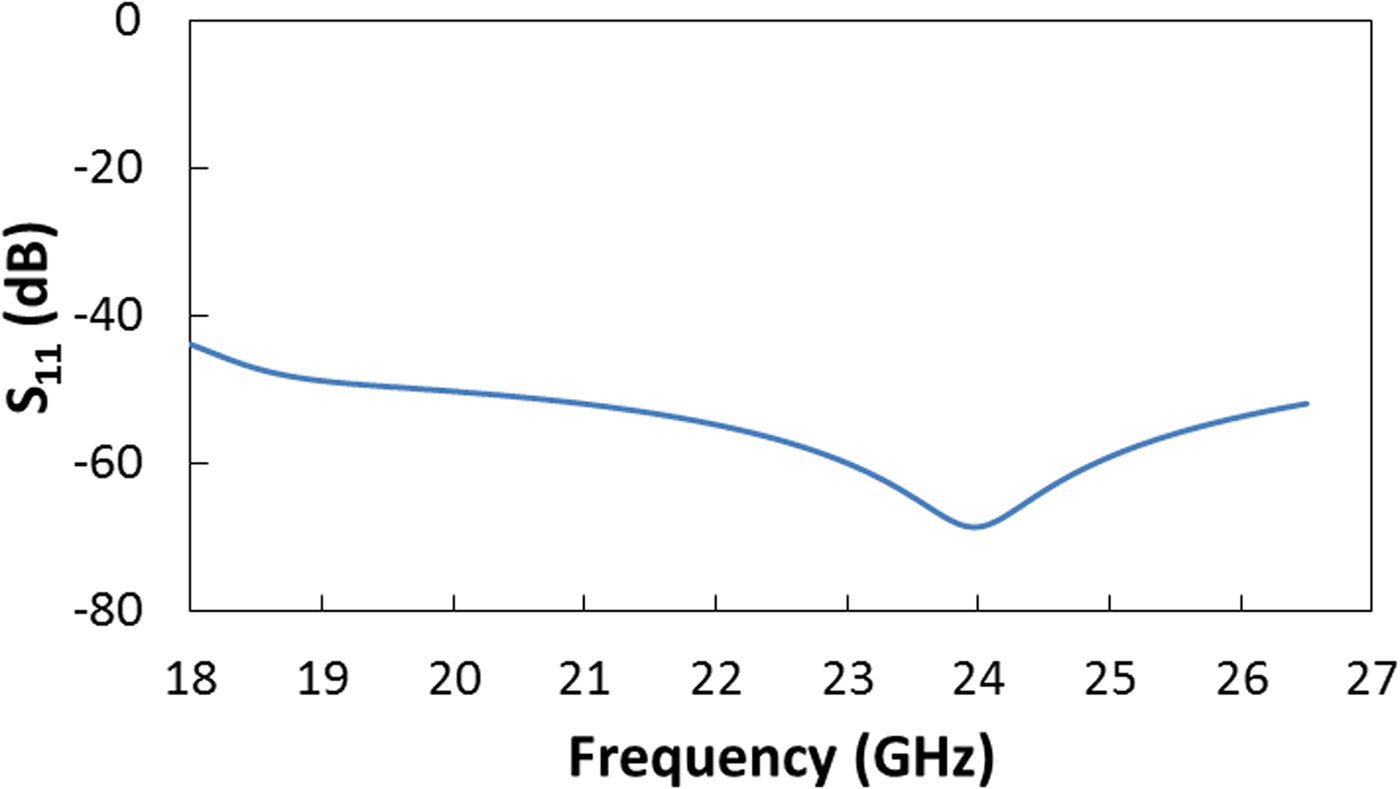
Fig. 6. Amplitude of the reflection level (S 11) of the selected ATW structure (a p = 1.2 mm, b p = 0.9 mm) between 18 and 26.5 GHz.
Table 1. Dimensions of the ATW geometry (in mm) used to realize microwave terminations.

III. 3D PRINTING PROCESS
A RepRap Asimov 3D printer was used to realize the devices. 3D models were extracted from the electromagnetic simulator. Slic3r software was then used to convert these models into printable files (conversion of the 3D model into horizontal layers).
Several printing parameters affect the quality of the printed devices, especially the compliance with expected dimensions, the presence of defects and the roughness. The main parameters studied here were bed and nozzle temperatures, printing and extrusion speeds and meshing. In our case, a bed temperature of 110 °C and a nozzle temperature of 230 °C appeared to be the best conditions. Printing instructions, defined during the conversion of the 3D model, allow the definition of the direction of printing, the thickness of each layer e lay, the width of the contour w cont, and the internal density of the object d int which is dependent on the meshing (Fig. 7). Moreover, in our case, we chose to give the upper and lower part of the devices a set thickness of three individual layers. The width of the contour w cont was 1 mm for all the printed devices. ATW geometries were printed in the b direction. It should be noted that the contour and the upper and lower layers have a density of 100%, whereas the density of the internal part of the object can be modified.
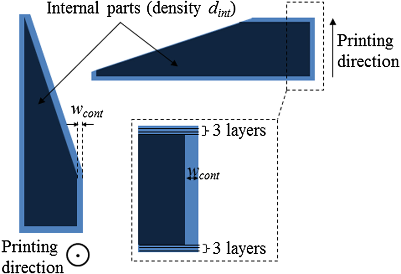
Fig. 7. Illustration of the 3D printing parameters used during the construction.
We first studied the effect of the internal density on the reflection parameter of the microwave termination, looking at density values (d int) from 50 to 100%. In this case, the thickness of each layer was set at 100 µm.
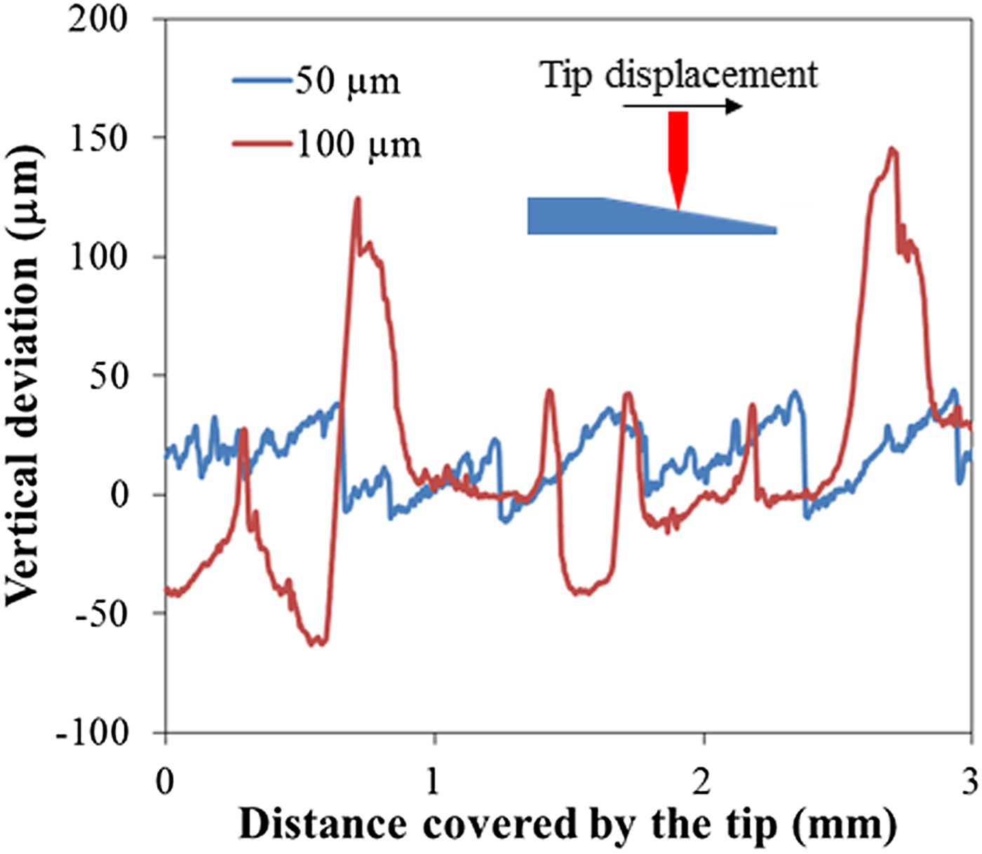
Next, we studied the reproducibility by realizing six ATW geometries with an internal density of 100% and a layer thickness e lay of 50 µm. Under these conditions, the devices had no random defects and a reduced surface roughness compared with those with a thickness layer of 100 µm, as shown in Fig. 8. Even if production time of printed absorber is longer, in this case, this parameter leads to more reproducible objects.
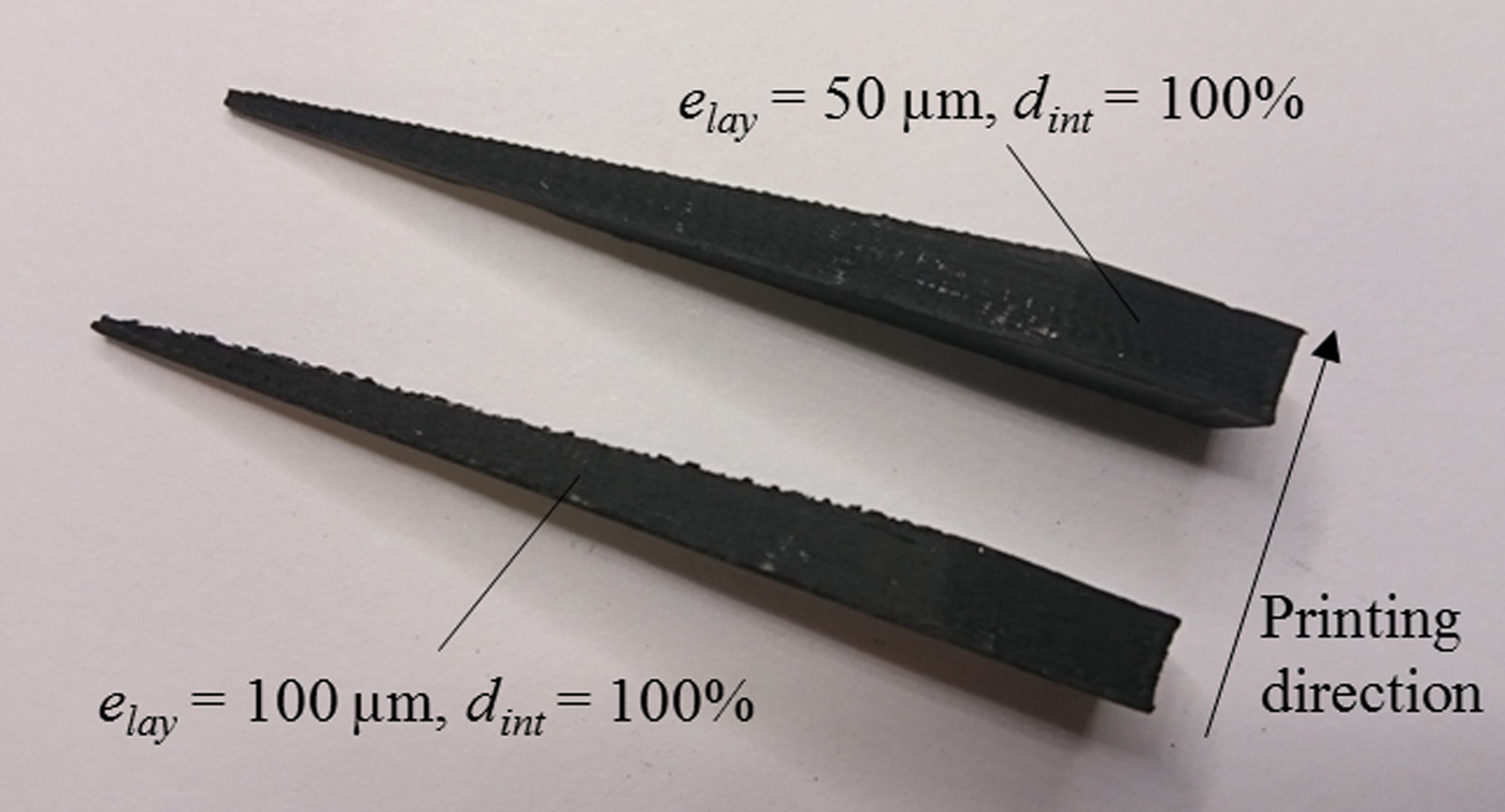
Fig. 8. Comparison of 3D-printed ATW geometries with layer thicknesses of 50 and 100 µm.
Surface roughness characterizations were performed using a stylus profiler system (Veeco Dektak 150). Figure 9 compares the vertical deviation measured along the tip of the ATW geometry for two different layer thicknesses (50 and 100 µm). When a layer thickness of 50 µm is chosen during the 3D-printing process, the vertical deviation shows quite a smooth behavior, with regularly positioned steps. A layer thickness of 100 µm leads to a rough surface with randomly positioned steps. The arithmetic average of the vertical deviation R a and root mean square of the vertical deviation R q are compared in Table 2 for the two different layer thicknesses. These values are the mean values of at least ten measurements performed on different samples and different positions on the wedge, so that standard deviation (σ Ra and σ Rq) can be calculated. R a value was about 4 times higher for a layer thickness of 100 µm (R a100μm = 37.4 µm). Moreover, the standard deviation of R a was very high (σ Ra = 27.6 µm), revealing the random distribution of the roughness over the surface of the device. As a comparison, a layer thickness of 50 µm led to R a = 10.7 µm and σ Ra = 2.3 µm, thus demonstrating that, in this case, the surface roughness was reduced and quite similar for the different samples.

Fig. 9. Comparison of the vertical deviation measured along the absorber tip for two different layer thicknesses (50 and 100 µm).
Table 2. The measured surface roughness of the ATW geometry for two different layer thicknesses.

One should note that no post-machining of the ATW geometries was performed so that reproducibility of S 11 between different 3D-printed terminations could be investigated.
IV. CHARACTERIZATION OF TERMINATIONS
Microwave terminations were characterized using a Vector Network Analyzer (VNA Agilent E8364A). 3D-printed loads were inserted into a WR42 short-circuited waveguide section and coaxial-to-rectangular waveguide transitions were used to connect the VNA to the microwave termination (Fig. 10).
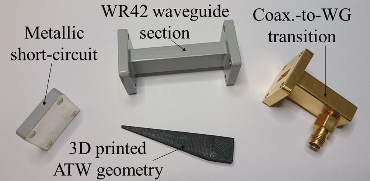
Fig. 10. Exploded view of the microwave termination.
A Thru-Reflect-Line calibration was performed in the 18–26.5 GHz frequency band in order to place the reference plane of measurement at the end of the coaxial-to-waveguide transition. Then, S 11 parameter was measured in order to evaluate the performance of the microwave terminations as a function of the printing parameters.
Expanded uncertainty of the measured reflection parameters was calculated by a similar approach to the one used in [Reference Arbaoui7] and detailed in [Reference Nazoa and Ridler8]. After calibration, we measured a residual directivity D = −46 dB and a residual test port match M = −63 dB that lead to expanded uncertainty U(RL) = 1.9 dB and U(RL) = 6.1 dB for measured reflection parameter levels of −30 and −40 dB, respectively.
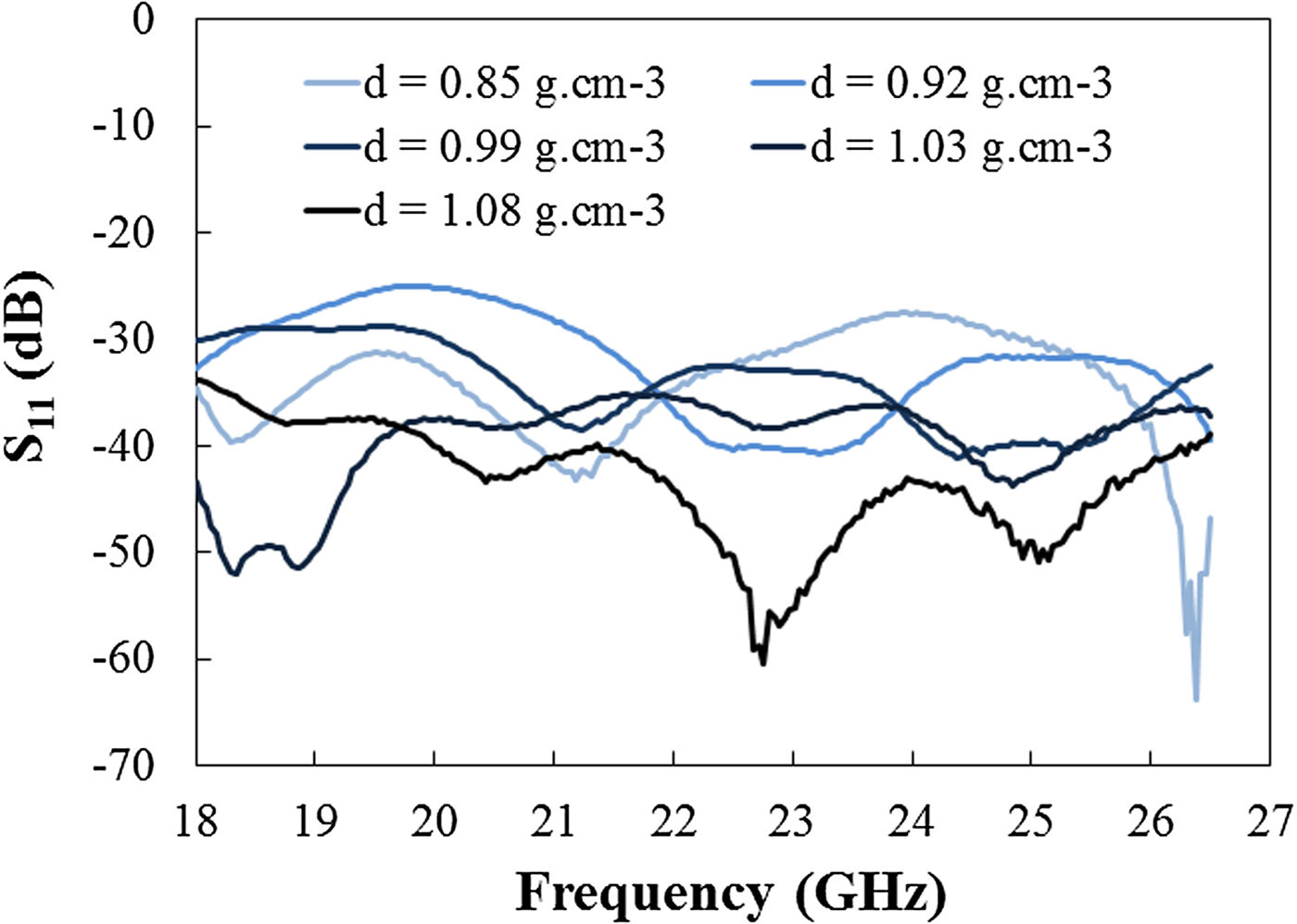
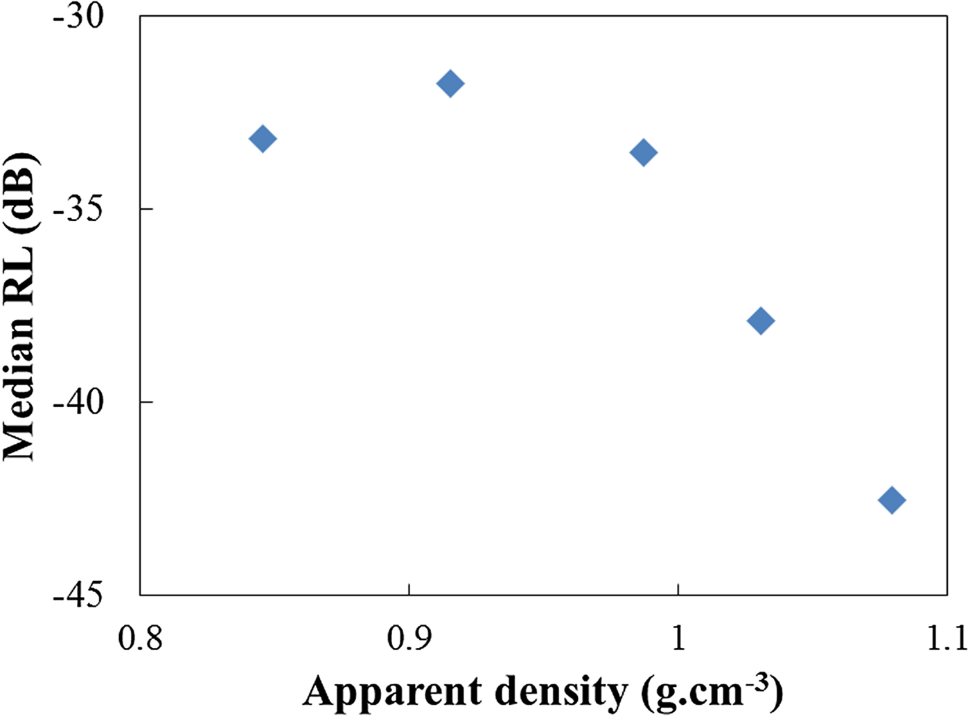
We first studied the effect of the internal density on the reflection parameter of microwave terminations. As the density of the contour, upper and lower layers and the internal part of the object can be different, we measured the apparent density of each of the ATW geometries by measuring their mass and knowing that the volume of the object is 1.189 cm3. When the internal density was increased from 50 to 100%, the apparent density increased from 0.85 to 1.08 g cm−3.
Figure 11 shows the reflection level of the microwave termination as a function of frequency for different values of apparent density. The denser geometry (d = 1.08 g cm−3) makes it possible to obtain a reflection level lower than 34 dB over the whole K-band. Logically, an ATW geometry with an apparent density of 0.85 g cm−3 should give worse performance. However, in this case, return losses remain lower than −27.5 dB between 18 and 26.5 GHz.

Fig. 11. Measured reflection parameter (S 11) amplitude as a function of frequency for different apparent densities of the ATW geometry (e lay = 100 µm).
We calculated the median value of return losses over the K-band for the different values of apparent density (Fig. 12). The median value of return losses is quite constant up to an apparent density of 0.98 g cm−3 and then decreases quasi-linearly. The denser geometry gives a median value of −42.5 dB. A monotonic decrease of reflection level as a function of the apparent density was expected. This unexpected evolution could be due to the automatic meshing of Slic3r software for which the positions or hollows at low density are not controlled.

Fig. 12. Evolution of the median value of return loss as a function of apparent density (e lay = 100 µm).
We then studied the reproducibility of the performance of these microwave terminations: six ATW geometries were printed under the same conditions (e lay = 50 µm, d int = 100%) and measured. Figure 13 presents the reflection coefficients of these microwave terminations as a function of frequency. We observed some noticeable differences of reflection coefficient between the six different 3D-printed ATW loads. However, the reflection coefficient is very sensitive to the presence of air gaps between the absorber and the metallic short circuit and it seems that this phenomenon could be mainly due to the manner of insertion of the ATW geometry in the short-circuited waveguide. In the worst case, reflection coefficient remains below −33.5 dB over the whole frequency band. Moreover, as one should recall, no post-machining was performed on the ATW geometries.
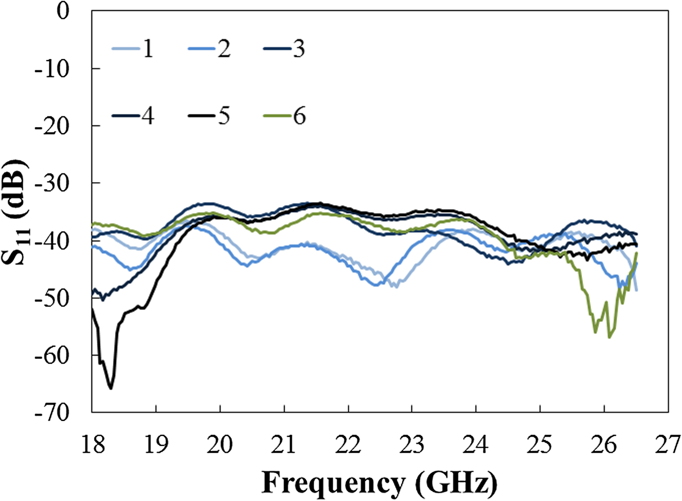
Fig. 13. Measured reflection parameter (S 11) amplitude as a function of frequency for six different ATW geometries printed in the same conditions (e lay = 50 µm, d int = 100%).
The median value of reflection coefficient is between −36.6 and −41.4 dB for these different devices (Fig. 14). The small difference in reflection parameter between the terminations supports the reproducibility of this new method of fabrication for microwave terminations.
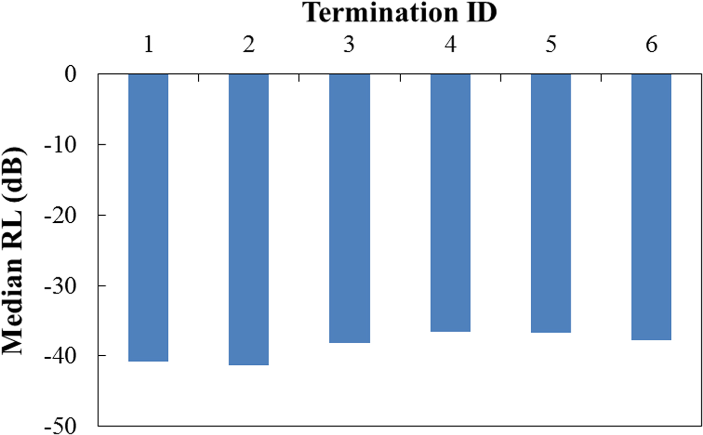
Fig. 14. Median value of reflection coefficient for six different ATW geometries printed in the same conditions (e lay = 50 µm, d int = 100%).
One should note that the median value of reflection level of ATW geometries printed with a thickness layer of 50 µm was slightly higher than the one of the geometry printed with a thickness layer of 100 µm. This difference can be mainly explained by a mean apparent density that is about 8% lower when a thickness layer of 50 µm is chosen. This difference of density is not yet clearly explained but could be due to meshing issues.
It is well known that 3D-printed objects are subject to moisture absorption, which can modify their dielectric properties, i.e., increase both permittivity and loss tangent [Reference Leite, Varanda, Silva, Relogio Ribeiro and Vaz9]. These objects can become water-impermeable when post-treatments, such as brushing or acetone sealing, are applied [Reference Nazoa and Ridler8]. In our case, no post-treatments were applied to the 3D-printed devices.
We selected an ATW insert and left it exposed to air for 45 days before taking measurements (Step 1 on Fig. 15). Then, we placed the device in an oven at 70 °C for 48 h before taking measurements once more (Step 2 on Fig. 15). We observed a slight difference between the measurement before and after drying at 70 °C during 48 h. For example, at 20 GHz, reflection level after drying is 4.5 dB lower than before drying. However, this difference remained lower than the uncertainty of measurement calculated for this low level of reflection parameters (U(RL = −40 dB) = 5.5 dB). As a consequence, it appears to be difficult to ascribe the observed difference in performance to moisture absorption. The effects of aging (especially water absorption) will next be investigated, by applying temperature and humidity cycles to the devices in a climate chamber.
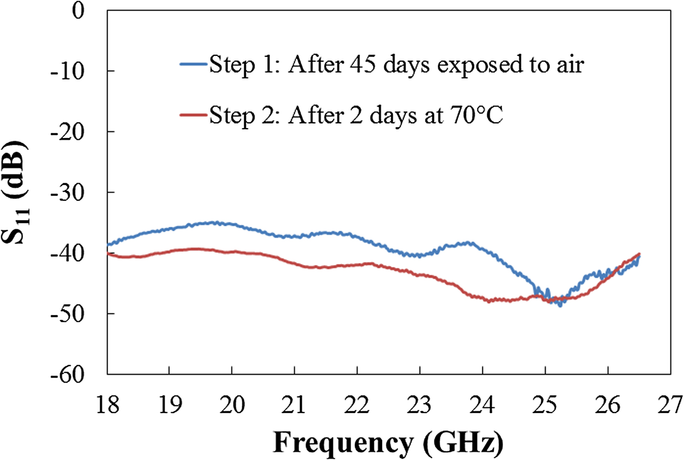
Fig. 15. Measurement of an ATW geometry after 45 days exposure to air (Step 1) and after 48 h at 70 °C (Step 2).
V. CONCLUSION
In this paper, we studied the realization of a K-band rectangular waveguide by 3D-printing technology. An ATW geometry was selected to design the absorber load. Indeed, this geometry is less sensitive to defects and truncation of the tip than a classic centered pyramidal load, and thus leads to more reproducible devices. Moreover, it appears to be more suited to 3D-printing technology (three different possible directions of printing without the need for support materials).
We then studied the effect of the ATW density on the reflection parameter of the microwave termination. It comes as no surprise that the performance of the microwave termination is strongly dependent on the density of the 3D-printed ATW load. However, even for a low-density value, reflection level was kept below −27.5 dB over the whole K-band (18–26.5 GHz).
Finally, we studied the reproducibility of the performances. Six ATW loads were printed under the same conditions and characterized. We experimentally proved that, without any post-machining of the 3D-printed ATW geometries, a maximum level of −33.5 dB can be ensured between 18 and 26.5 GHz. This suggests the 3D-printing process of absorbing materials is repeatable and that it is suitable for the realization of microwave terminations in an industrial context. Given these results, we estimate that this concept can be applied to the realization of microwave termination up to 50 GHz (WR22 rectangular waveguide). Above this frequency, rectangular waveguide dimensions are so small that the resolution of FDM technology seems to be too low to ensure the respect of the dimensions of the printed absorber, and thus, a satisfactory reproducibility. Owing to a better resolution, stereolithography technique appears to be a way to shape microwave absorber at very high frequencies. However, new materials with dedicated properties (i.e., high loss tangent) have to be developed.
Power handling capability is one of the key points to be investigated in order to evaluate the potential of this technology for industrial applications, especially for integration into space systems. This point will be one of our main subjects of research in the future.
Furthermore, self-supported 3D-printed microwave terminations (absorber insert, short-circuit, and waveguide flange in a single printed device) will be soon designed and fabricated in the K-band. As was demonstrated in [Reference Arbaoui7], microwave response of such devices can be as high as standard microwave terminations but offer the advantages of very low cost and weight.
Acknowledgement
This work was supported by the French Directorate General of Armaments (DGA) in the framework of the ANR ASTRID 3DRAM.
 Azar Maalouf was born in 1975 in Lebanon, he earned an engineering degree in materials science in 2001 from Polytech Nantes, France. He earned his Ph.D. in physics in 2007 from the University of Rennes 1, France. In 2011, he became a research engineer at the University of Brest, France. His main scientific interests are the physical chemistry of materials, particularly the study and the implementation of these materials in thin, thick or massive layers. The fields of application include rechargeable batteries and accumulators (2001–2003), study and fabrication of optical waveguides and optical communications (2003–2010), and the study and fabrication of circuits operating in the domains of microwaves (2011–present).
 Ronan Gingat is a 5th-year student in materials science at INSA Rennes. Before joining INSA, he studied for 2 years (2012–2014) in an integrated preparatory class at ESIR (University of Rennes 1). In 2016, he did an internship at Lab-STICC on the topic covered in this paper, working on the 3D printer to optimize the printing conditions of carbon-loaded Acrylonitrile Butadiene Styrene (ABS).
 Vincent Laur received his Ph.D. degree in electronics from the University of Brest, France, in 2007. During his degree, he investigated the potential of ferroelectric thin films for the realization of microwave tunable devices. In 2008, he was a post-doctoral fellow at XLIM laboratory (Limoges, France) where he worked on the design and realization of ferroelectric- or MEMS-based tunable devices. He is currently an Assistant Professor at the Lab-STICC laboratory, Brest, France. His research interests are focused on the characterization, modeling, and integration of functional materials (ferroelectrics, ferromagnetics, ferrites…) for microwave applications. He also works on the application of new technologies (3D printing, 3D metallization, Molded Interconnect Devices, nanomaterials…) to the microwave domain.