


I. INTRODUCTION
Integrated dielectric lens antennas (ILAs), also referred to as substrate lens, are widely used in various communication, radar, and imaging systems, especially in the millimeter (mm) and sub-mm wave bands [Reference Yin and Dou1]. This is because the major drawbacks of traditional dielectric lens and planar antennas, such as low directivity and losses of power into surface waves, can be overcome when a dielectric lens is leaned against the planar antenna, the latter providing the primary focal source for the lens itself. This makes ILAs compatible with the integration in RF front-end circuits. Microstrip patch antennas/arrays commonly used in ILAs [Reference Yin and Dou1–Reference Tinh Nguyen, Sauleau and Le Coq4] however are unsuitable for application at the millimeter wave band because they possess higher ohmic losses in these high frequencies.
Over the last few decades, substrate-integrated waveguide (SIW) technology has been widely used in the design of numerous structures and antennas from microwave to sub-mm wave bands [Reference Bozzi, Georgiadis and Wu5, Reference Bayderkhani, Forooraghi and Abbasi-Arand6]. The use of SIW-based slot antenna/array to feed dielectric lens in ILAs is becoming very attractive at these frequency bands.
There are many instances in recent literature discussing the methods for analyzing ILAs using various numerical approaches commonly based on geometrical optics, physical optics (PO) principles [Reference Godi, Sauleau, Le Coq and Thouroude2–Reference Tinh Nguyen, Sauleau and Le Coq4], and finite difference time domain (FDTD) method [Reference Godi, Sauleau and Thouroude7, Reference van der Vorst and de Maagt8]. Moreover, SIW circuits have been designed and analyzed using approximate analytical methods based on transmission-line theory [Reference Kishihara, Yamane and Ohta9], the equivalent-waveguide-width model [Reference Deslandes, Perregrini, Arcioni, Bressan, Wu and Conciauro10], two dimensional, multi-port methods [Reference Abaei, Mehrshahi, Amendola, Arnieri and Shamsafar11] or finite-element (FEM) and finite-difference (FD)-based commercial full-wave solvers. The former approach is computationally efficient, but it does not guarantee the accuracy of the final design results. The latter approach can be very time consuming and memory exhaustive especially for large and complex structures. Hence, an efficient full-wave analysis technique is required in order to investigate general ILA structures fed using SIW slot antenna/array.
In this paper, a very fast and highly efficient full-wave technique is proposed for analyzing an ILA structure fed by SIW-based slot antenna/array. The approach in [Reference Arnieri and Amendola12] has been extended to analyze a double-layered SIW slot antenna/array with arbitrary number of radiating and/or coupling slots. In addition, to predict the effects of dielectric lens on the SIW antenna, the dielectric lens is analyzed using Ray/PO technique. Finally, the equations with the unknowns are solved to obtain the equivalent surface currents on the aperture of slots. The proposed technique is validated by applying it to a hemispherical ILA fed by a double-layered SIW-based cavity-backed slot antenna. Comparison between the proposed technique and FEM using HFSS are presented, which show the proposed technique is exceptionally efficient in terms of computational time and storage capacity, as well as numerical accuracy.
II. PROBLEM FORMULATION
The solution domain is split into three distinct regions, as shown in Fig. 1, which are connected by the unknown magnetic currents M. Method-of-moments (MoM) regions R0 and R1 are include a generic SIW circuit with arbitrary number of coupling/radiating slots and posts excited through coaxial/waveguide ports. R2 is the PO region away from the antenna containing a dielectric lens which is stacked on the top wall of the antenna and characterized by the constitutive parameters ε
d
and μ
d
. Bo2 denotes the boundary surface between R1 and R2, and Bo1 is the boundary between R0 and R1. The coupling slots are located on Bo1, while the radiating slots are placed on Bo2. The normal vector
 ${\hat n_{i + 1}}$
points into the region Ri. Parallel plates that form the SIW structure are assumed to be a perfect-electric conductor with infinitesimal thickness. Only one excitation is considered here however if several feeding ports are present their effects would be superposed. Excitation port generates the field in R0 and the same time the field in R1 is excited by the coupling slots placed on Bo1.
${\hat n_{i + 1}}$
points into the region Ri. Parallel plates that form the SIW structure are assumed to be a perfect-electric conductor with infinitesimal thickness. Only one excitation is considered here however if several feeding ports are present their effects would be superposed. Excitation port generates the field in R0 and the same time the field in R1 is excited by the coupling slots placed on Bo1.

Fig. 1. Schematic view of an ILA fed by double-layered SIW slot antenna. Also shown is an entire domain basis function shape used to expand the unknown magnetic current on the slot with corresponding parameters.
In order to model the double-layered SIW-based slot antenna (internal region) MoM along with mode matching technique are necessary. This is done by representing the field in the post-walled structure through the Dyadic Green's function of the parallel plate waveguide [Reference Arnieri and Amendola13, Reference Amendola, Arnieri and Boccia14]. By invoking the field-equivalence principle, the slots are replaced by a metal plate and equivalent magnetic currents (M inner and M outer ) are introduced on their respective surfaces. Due to the use of narrow rectangular slots it can be assumed that there are only transverse electric field components across the slots, and the magnetic current is completely directed along the longitudinal direction and its transverse dependence is negligible. Applying the boundary conditions on the aperture of slots requires the tangential electric and magnetic fields to be continuous. The continuity of tangential electric fields leads to the equality M inner = −M outer = M, as shown in Fig. 1, whereas the continuity of magnetic field across the surface S of the slots leads to the following general integral equation for each slot i [Reference Bayderkhani, Forooraghi, Arnieri and Abbasi-Arand15]:
 $${\mathop{n}^{\frown}} \times H_{tot}^{inner} (r) = {\mathop{n}^{\frown}} \times H_{tot}^{outer} (r),$$
 $$\eqalign{\hat n \times & \left( {H_{inc}^{inner} (r) + \sum\limits_j^{Ns} {H_{M\_slot\_j}^{inner}} (r)} \right). \cr & = \hat n \times \left( \matrix{H_{inc}^{outer} (r) + \hfill \cr + \sum\limits_j^{Ns} {H_{M\_slot\_j}^{outer}} (r) + \sum\limits_q^{Nq} {\sum\limits_j^{Ns} {H_{jq}^{Po} (r)}} \hfill} \right)r \in {S_i}} $$
In which [Reference Arnieri and Amendola12]
 $$\eqalign{& {H_{inc}}(r) = \cr & \quad - j\omega {\varepsilon _0}{\varepsilon _r}\int_{{V_{SRC}}} {{{\bar G}_{PPW}}(r,r^{\prime})} \cdot {M_{SRC}}(r^{\prime})dr^{\prime} + H_S^{{M_{SRC}}} (r),} $$
 $$\eqalign{& {H_{M\_slot,j}}(r) = \cr & \quad - j\omega {\varepsilon _0}{\varepsilon _r}\int_{{S_j}} {{{\bar G}_{PPW}}(r,r^{\prime})} \cdot {M_j}(r^{\prime})dr^{\prime} + H_S^{{M_j}} (r),} $$
where r and r′ define the observation and source points, respectively; N s is the number of slots; Nq is the number of modes used to expand the current on the slot.
M
j
is the equivalent magnetic current source defined on surface of slot j (Sj);
 ${\bar G_{PPW}}(r,r')$
is the Dyadic Green's function of the parallel plate waveguide when all the slots are absent (see Appendix A);
${\bar G_{PPW}}(r,r')$
is the Dyadic Green's function of the parallel plate waveguide when all the slots are absent (see Appendix A);
 $H_S^M $
is the field scattered by the metallic posts due to the current M; M
SRC
(r
′) is the magnetic current source distribution defining the port excitation in volume V
SRC
located in region R
0; and HPO
is the magnetic field pre-computed by Ray/PO technique to model the dielectric lens effects, and it has non-zero value only for outer region. To do so, the equivalence principle is applied on the lens surface and the forward as well as backward radiation is calculated. The total field in the external region is then obtained by the summation of incident fields impinging from the antenna and scattered fields from the lens boundary. Surface integration equation was established on the aperture of slots. Finally, the equations with the unknowns are solved to obtain the equivalent surface currents on the aperture of slots. In the application of (2), it should be noted that in each region only corresponding slots should be considered, for example in R0 the radiating slots are vanished.
$H_S^M $
is the field scattered by the metallic posts due to the current M; M
SRC
(r
′) is the magnetic current source distribution defining the port excitation in volume V
SRC
located in region R
0; and HPO
is the magnetic field pre-computed by Ray/PO technique to model the dielectric lens effects, and it has non-zero value only for outer region. To do so, the equivalence principle is applied on the lens surface and the forward as well as backward radiation is calculated. The total field in the external region is then obtained by the summation of incident fields impinging from the antenna and scattered fields from the lens boundary. Surface integration equation was established on the aperture of slots. Finally, the equations with the unknowns are solved to obtain the equivalent surface currents on the aperture of slots. In the application of (2), it should be noted that in each region only corresponding slots should be considered, for example in R0 the radiating slots are vanished.
The equivalent magnetic currents, which are used to model the slots, are expanded in terms of an entire domain sinusoidal basis function. The magnetic currents for a slot j are:
 $${M_j}(r^{\prime}) = {\hat v_j}\sum\limits_q {{f_{q,j}}(r^{\prime}) \cdot {V_{q,j}}\quad 1 \le j \le {N_s}}, $$
 $${f_{q,j}}(r^{\prime}) = \sin \left( {{k_q}\left( {\displaystyle{{{L_j}} \over 2} + {\nu _j}} \right)} \right),\quad \vert {\nu _j} \vert \le {L_j},$$
 $${k_q} = \displaystyle{{q\pi} \over {{L_j}}}\quad {\rm and}\quad r^{\prime} = {r_{jq}} + u{\hat u_j} + v{\hat v_j},$$
where r jq , V q,j and L j are defined as the center of the qth basis function on the slot j, the unknown expansion coefficients and the length of the jth slot, respectively, as shown in Fig. 1, and q spans over the number of modes Nq.
The integral equation (2) is solved using the Galerkin weighting procedure where equations (3)–(7) are substituted into (2). After some mathematical manipulations, the following linear system with N s × N q unknowns is obtained:
 $${h_{p,i}} = \sum\limits_{q,j} {Y_{q,j}^{p,i} \cdot {V_{q,j}}\quad \forall (p,i)}, $$
where p and q span over the basis functions, while i and j span, the number of slots, NS.
 $${h_{p,i}} = \left\{ {\matrix{ {\int_{{S_i}} {{f_{p,i}}{{\hat v}_i} \cdot {H_{inc}}(r)dr}} & {{\rm for}\;{\rm interior}\;{\rm region,}} \cr 0 & {{\rm other}\;{\rm regions,}} \cr}} \right.$$
 $$Y_{q,j}^{p,i} = Y_{q,j}^{p,i} (int1) + Y_{q,j}^{p,i} (int2) + Y_{q,j}^{p,i} (ext),$$
 $$\eqalign{& Y_{q,j}^{p,i} (ext) = \cr & \quad \left\{ {\matrix{ j\omega {\varepsilon _0}{\varepsilon _d}\int_{{S_i}} {dr} \int_{{S_j}} dr^{\prime}{f_{p,i}}{{\hat v}_i} \cdot {{\bar G}_{ext}}(r,r^{\prime})\cr \cdot {{\hat v}_j}{\,f_{q,j}} + \int_{{S_i}} {dr} {f_{p,i}}{{\hat v}_i} \cdot {H^{PO}}(r) & {{\rm for}\;{\rm radiating}\;{\rm slots,}} \cr 0 & {{\rm otherwise,}} \cr}} \right.} $$
 $$\eqalign{Y_{q,j}^{p,i} (int) = & j\omega {\varepsilon _0}{\varepsilon _r} \cdot \cr & \quad \int_{{S_i}} {dr} \int_{{S_j}} {dr^{\prime}} {f_{p,i}}{{\hat v}_i} \cdot {{\bar {G}}_{PPW}}(r,r^{\prime}) \cdot {{\hat v}_j}{\,f_{q,j}} \cr & \quad + \int_{{S_i}} {dr{f_{p,i}}} {{\hat v}_i} \cdot H_S^{{f_{q,j}}} (r),} $$
where
 $Y_{q,j}^{p,i} (int{\rm 1})$
and
$Y_{q,j}^{p,i} (int{\rm 1})$
and
 $Y_{q,j}^{p,i} (int{\rm 2})$
are the admittance elements in R0 and R1 regions, respectively, that have the same form of (12). G
ext
is the Dyadic Green's function for the external region [Reference Arnieri and Amendola12]. The incident magnetic field radiating into the structure by a port source in the absence of the slots is defined by H
inc
(r). In the above formulation, only one port source which is radiated in the interior region is assumed. As mentioned earlier, if several feeding ports are presented, their effects need to be superposed. Consequently, the number of unknowns is given by the number of modes assumed in each slot (Nq) multiplied by the number of slots (N
S
), i.e. Nq × Ns. As a result, the computational efficiency is achieved along with reasonable accuracy using the proposed hybrid method.
$Y_{q,j}^{p,i} (int{\rm 2})$
are the admittance elements in R0 and R1 regions, respectively, that have the same form of (12). G
ext
is the Dyadic Green's function for the external region [Reference Arnieri and Amendola12]. The incident magnetic field radiating into the structure by a port source in the absence of the slots is defined by H
inc
(r). In the above formulation, only one port source which is radiated in the interior region is assumed. As mentioned earlier, if several feeding ports are presented, their effects need to be superposed. Consequently, the number of unknowns is given by the number of modes assumed in each slot (Nq) multiplied by the number of slots (N
S
), i.e. Nq × Ns. As a result, the computational efficiency is achieved along with reasonable accuracy using the proposed hybrid method.
III. SIMULATION
In order to validate the proposed technique it was applied to a hemispherical ILA fed by a double-layered SIW-based cavity-backed slot antenna. A comparison between the proposed method and finite-element simulations carried out using Ansoft's HFSS are presented and discussed.
A) Input impedance and radiation pattern
The geometry of the hemispherical ILA fed by double-layered SIW cavity-backed slot antenna is shown in Fig. 2, and the corresponding parameters shown in Fig. 3. The SIW antenna structure consists of two main building blocks consisting of the feeding system and the radiating system, as shown in Fig. 3. The feeding and the radiating systems are implemented on two different substrate layers. The vertical walls of structure are realized using rows of metalized posts embedded in a dielectric substrate (RO4003TM) with a relative permittivity of 3.55, a loss tangent of 0.0027, and a thickness of 10 mil. The radiating system includes a main cavity, where the radiating slots are etched on the top side of the metal, as shown in Fig. 2.
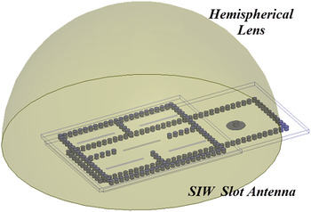
Fig. 2. Representation of the entire hemispherical lens antenna.
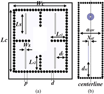
Fig. 3. Feeding SIW slot antenna including: (a) cavity and radiating slots placed on top of the substrate, and (b) feeding waveguide and coupling aperture placed on the bottom of the substrate.
The cavity is divided into four sub-sections with a radiating slot on the top wall of each sub-section. In order to excite the cavity, a feeding short-circuited SIW waveguide on the rear side of the cavity is used. In order to connect two layers, a coupling longitudinal slot transition located in the common face of two SIW blocks is used. This antenna radiates into a hemispherical dielectric lens with constitutive parameters ε d = 2.1 and μ d = 1 and radius of R DL = 50 mm. The antenna parameters and their corresponding values are listed in Table 1. Figure 4(a) shows the reflection coefficient of the antenna compared with results obtained from HFSS. The phase of the reflection coefficient of the antenna is depicted in Fig. 4(b). The total field pattern of the antenna is shown in Fig. 5. The results indicate that the proposed method agrees very well with the results using HFSS. It should be noted that by tuning the ILA parameters, better matching is achievable. In order to show the dielectric lens effects on the input impedance of the antenna, the impedance with and without dielectric lens is computed and shown in Fig. 6; from this figure, it is found that the input impedance of the antenna is strongly altered due to the presence of lens.

Fig. 4. Reflection coefficient of the ILA compared with HFSS, (a) magnitude and (b) phase.

Fig. 5. Total field pattern of the ILA computed using the proposed technique and HFSS in (a) φ = 0 plane and (b) φ = 90 plane.

Fig. 6. Impact of dielectric lens on the input impedance of the SIW slot antenna obtained by using MoM–PO method (solid lines show the Z11 with lens effects, and dash lines show Z11 without lens effects).
Table 1. Antenna parameters and corresponding values.

B) CPU time and storage requirements
The hybrid method described in the present paper requires three matrices to be filled and inverted. In the PO region, a matrix needs to be filled in order to compute the PO currents on the lens surface.
The matrix dimension depends on the number of points assumed in order to compute the PO currents. In the MoM region, two matrixes need to be filled, where one of them used to compute the field scattered by the metallic vias and the other one to evaluate the unknown magnetic currents over the slots.
The size of the matrix in the PO region depends on the area that is illuminated by the antenna beam, and the number of mesh cells depends on the computational area. By increasing the number of mesh cells the accuracy of the PO fields and consequently the CPU processing time and memory requirements are increased. The simulated results indicate that a λ g /10 × λ g /10 mesh cell size covering the illuminated area is sufficient to ensure the accuracy of the calculated PO fields. In the MoM region, the number of cylinders NC, the number of slots Ns and the number of Z modes Nz define the size of two matrixes.
Table 2 and 3 report the CPU processing time and memory storage used in simulating the hemispherical ILA fed by the double-layered SIW cavity-backed slot antenna, respectively.
Table 2. CPU time (Intel Core i7 3.55 GHz, 16 GB RAM).

Table 3. Memory requirement.

Comparison of the CPU time and storage capacity of the proposed technique with HFSS shows substantial reduction is achieved with the proposed technique, i.e. CPU time is reduced by around 95% and memory capacity is reduced by around 96%. Consequently, the proposed technique raises possibility of simulating larger and more complex structures such as multilayered SIW-based antennas with limited computing resources with acceptable numerical accuracy.
IV. CONCLUSION
A very fast and highly efficient full-wave technique is proposed that is based on a hybrid MoM–PO implementation that enables rigorous analyzes of ILAs fed by SIW-based slot antenna/array. The technique was applied to analyze a hemispherical ILA fed by double-layered SIW cavity backed slot antenna. Excellent agreement is obtained between the proposed technique and commercial FEM-based solver such as HFSS. However, the proposed technique offers the advantage of providing a solution at a significantly shorter computational time frame with substantially lower storage requirements without compromising numerical accuracy.
 Reza Bayderkhani was born on February 10, 1985, in Tehran, Iran. He received both his B.Sc. and the M.Sc. degrees from the Shahed University, Tehran, Iran in 2007 and 2010, respectively and his Ph.D. (with honors) degree from Tarbiat Modares University (TMU), Tehran, Iran, in 2015, all in communication engineering. His research interests include computational electromagnetic, planar antenna structures and arrays, and SIW structures.
 Keyvan Forooraghi was born in Tehran, Iran. He received the M.Sc. degree, Technology Licentiate and Ph.D. from Chalmers University of Technology, Gothenburg, Sweden, in 1983, 1988, and 1991, respectively, all in electrical engineering. He was a researcher at the Department of Network Theory during 1992–1993. He joined the Department of Electrical Engineering at Tarbiat Modares University (TMU) in 1993 where he currently is a professor and lectures on electromagnetic, antenna theory and design, and microwave circuits. His research interests include computational electromagnetic, waveguide slot antenna design, and microstrip antennas.
 Emilio Arnieri was born in Cosenza, Italy, in 1977. He received the degree (with honors) in Information Technology Engineering from the University of Calabria, Rende, Italy, in 2003 and the Ph.D. degree in Electronic Engineering from the University “Mediterranea” of Reggio Calabria, in 2007. Currently, he is an Assistant Professor with the Department of Informatics, Modeling, Electronics and System Engineering (DIMES), University of Calabria (Italy). His main research activities concern the development of dual-band antennas and millimeter-wave components, development of numerical methods for the electromagnetic modeling of microwave, and millimeter-wave circuits (substrate-integrated circuits, slotted substrate-integrated waveguide arrays, and substrate-integrated waveguide resonators).
 Bijan Abbasi Arand received the B.Sc. degree from Shiraz University, Shiraz, Iran in 1995 and the M.S. and Ph.D. degrees in Telecommunication Engineering from Tarbiat Modares University, Tehran, Iran in 1997 and 2003, respectively. From 2003 to 2005, He was a researcher of Electromagnetic Propagation Department in Iran Telecommunication Research Centre (ITRC). In 2005, he joined the Satellite Communication Laboratory of Tarbiat Modares as a Postdoctoral researcher. Since 2010, he has been an Assistant Professor in the faculty of Electrical and Computer Engineering of Tarbiat Modares. He has more than 35 papers and publications in several journals and conferences.
 Bal Virdee graduated with a B.Sc. (Eng.) Honors in Communication Engineering and MPhil degree from Leeds University, UK. He obtained his Ph.D. degree from the University of North London, UK. He was worked as an academic at Open University and Leeds University. Prior to this he was an R & D Electronic Engineer in the Future Products Department at Teledyne Defence (formerly Filtronic Components Ltd., Shipley, West Yorkshire), and at PYE TVT (Philips) in Cambridge. He has held numerous duties and responsibilities at the university, i.e.: Health & Safety Officer, Postgraduate Tutor, Examination's Officer, Admission's Tutor, Short Course Organiser, Course Leader for M.Sc./M.Eng. Satellite Communications, B.Sc. Communications Systems, and B.Sc. Electronics. In 2010, he was appointed Academic Leader (UG Recruitment). He is a member of ethical committee, member of faculty's research committee, and research degrees committee.
APPENDIX A
The dyadic Green's function of the parallel plate waveguide has the following form [Reference Arnieri and Amendola13]:
 $$\eqalign{{{\bar G}_{PPW}}(r,r^{\prime}) = &- \displaystyle{1 \over {{k^2}}}\hat z\hat z\delta (r - r^{\prime}) - j\sum\limits_m {\left( {1 - \displaystyle{{{\delta _{m0}}} \over 2}} \right)} \displaystyle{1 \over {2k_{\rho m}^2 h}} \cr & \times \big[\big[ {\left( {\nabla \times \hat z} \right)} \left( {\nabla ^{\prime} \times \hat z} \right)H_0^{(2)} \left( {{k_{\rho m}}\left \vert {\rho - \rho ^{\prime}} \right \vert} \right){f_c}\left( {{k_{zm}},z,z^{\prime}} \right) \cr & + \displaystyle{1 \over {{k^2}}}\left( {\nabla \times \nabla \times \hat z} \right)\left( {\nabla ^{\prime} \times \nabla ^{\prime} \times \hat z} \right)H_0^{(2)} \cr & \times \left( {{k_{\rho m}} \vert {\rho - \rho ^{\prime}} \vert} \right)\,{f_s} {\left( {{k_{zm}},z,z^{\prime}} \right)} \big],}$$
with
 $k = \omega \sqrt {\mu {\varepsilon _0}\varepsilon} $
, k
zm
= mπ/h,
$k = \omega \sqrt {\mu {\varepsilon _0}\varepsilon} $
, k
zm
= mπ/h,
 ${k_{\rho m}} = \sqrt {{k^2} - k_{zm}^2} $
, and
${k_{\rho m}} = \sqrt {{k^2} - k_{zm}^2} $
, and
 $${{\delta _{m0}} = \left\{ {\matrix{ 1 & {{\rm for}\;m = 0,} \cr 0 & {{\rm for}\;m \ne 0,} \cr}} \right.}$$
 $${{f_{c,s}} = \left( {\matrix{ {\cos ({k_{zm}}z)\cos ({k_{zm}}z^{\prime}),} \cr {\sin ({k_{zm}}z)\sin ({k_{zm}}z^{\prime}),} \cr}} \right.}$$
where k is the wave number, k zm is the wave number in the z-direction, and k ρ m is the radial wave number.


