I. INTRODUCTION
Direct conversion receivers are used in Doppler radars for speed monitoring, vital signs detection, and measurements of ballistic targets. In these applications, using direct conversion gives the Doppler shift and thus the speed measurement directly from the received frequency. It is also common to use direct conversion to avoid complex image rejection structures in other applications [Reference Razavi1]. The key element in a direct conversion receiver is the mixer.
Mixers for direct conversion applications must have low 1/f-noise and leakage due to LO and RF which exists at the same frequency. Two fundamental types of direct conversion mixers exist, active and passive. Active mixers have the advantage of providing conversion gain, whereas passive mixers have the advantage of higher linearity and less noise. Structures for increasing linearity of the active mixers have been proposed [Reference Barati and Yavari2], but then suffer from increased noise. Thus, the dynamic range remains largest for a passive mixer design. The main disadvantage of the passive mixer is the loss in the signal path.
The double-balanced structure has the advantage of inherent isolation between all ports, good linearity, and broadband operation [Reference Maas3]. These are all desired characteristics for mixers to be used in Doppler radars. Having built-in isolation in the mixer structure is important, as normal filtering is difficult due to the proximity of the RF and LO frequencies. The drawbacks are increased circuit complexity, higher LO-power requirement, and higher conversion loss.
Using a CMOS process to realize the circuit has the advantage of low-cost mass production. Unfortunately the MOSFET suffers from traps in the oxide, which leads to an increased 1/f-noise. Bipolar devices on the other hand are bulk conduction devices, which have an order of magnitude lower 1/f noise compared to the surface channel conduction of CMOS devices [Reference Babcock, Loftin, Madhani, Chen, Pinto and Schroder4].
In this paper, a direct conversion mixer operating at X-band that has characteristics optimized for Doppler radar applications is described. These characteristics include state-of-the-art linearity, together with good 1/f-noise performance and reasonable conversion loss. To meet these requirements, double-balanced passive mixer architecture is chosen. The circuit is fabricated using a SiGe:C BiCMOS process from Innovations for High Performance Microelectronics (IHP). It is a 0.25 µm technology, featuring high-performance npn-HBTs having a unit current gain frequency (f T) of 110 GHz and a maximum oscillation frequency (f max) of 180 GHz. The process has metal-insulator-metal (MIM) capacitors and five metal layers of which the upper two are extra thick, intended for passives or low loss interconnects [5].
As the SiGe HBT process used for implementation do not offer suitable diodes for mixing, diode-connected HBTs as in [Reference Issakov, Knapp, Wojnowski, Thiede and Simburger6] are used.
II. DESIGN
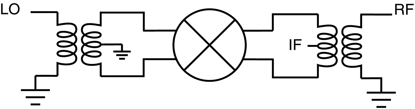
This section describes the design of the proposed double-balanced ring diode mixer. Diodes are desired for the implementation of low-noise mixers in direct conversion receivers. In many SiGe HBT technologies, there are no diodes available. Using the base–emitter junction of the high-speed HBTs available as a pn-junction diode [Reference Issakov, Knapp, Wojnowski, Thiede and Simburger6], it is possible to have good mixer diodes in a SiGe HBT technology. The design description is divided into three parts covering the design of the balun, the intermediate frequency (IF) extraction and the mixer core. Figure 1 shows a block diagram of the mixer circuit.

Fig. 1. Block diagram of the balanced mixer circuit. Showing LO and RF balun together with center tapped IF extraction.
A) Marchand balun
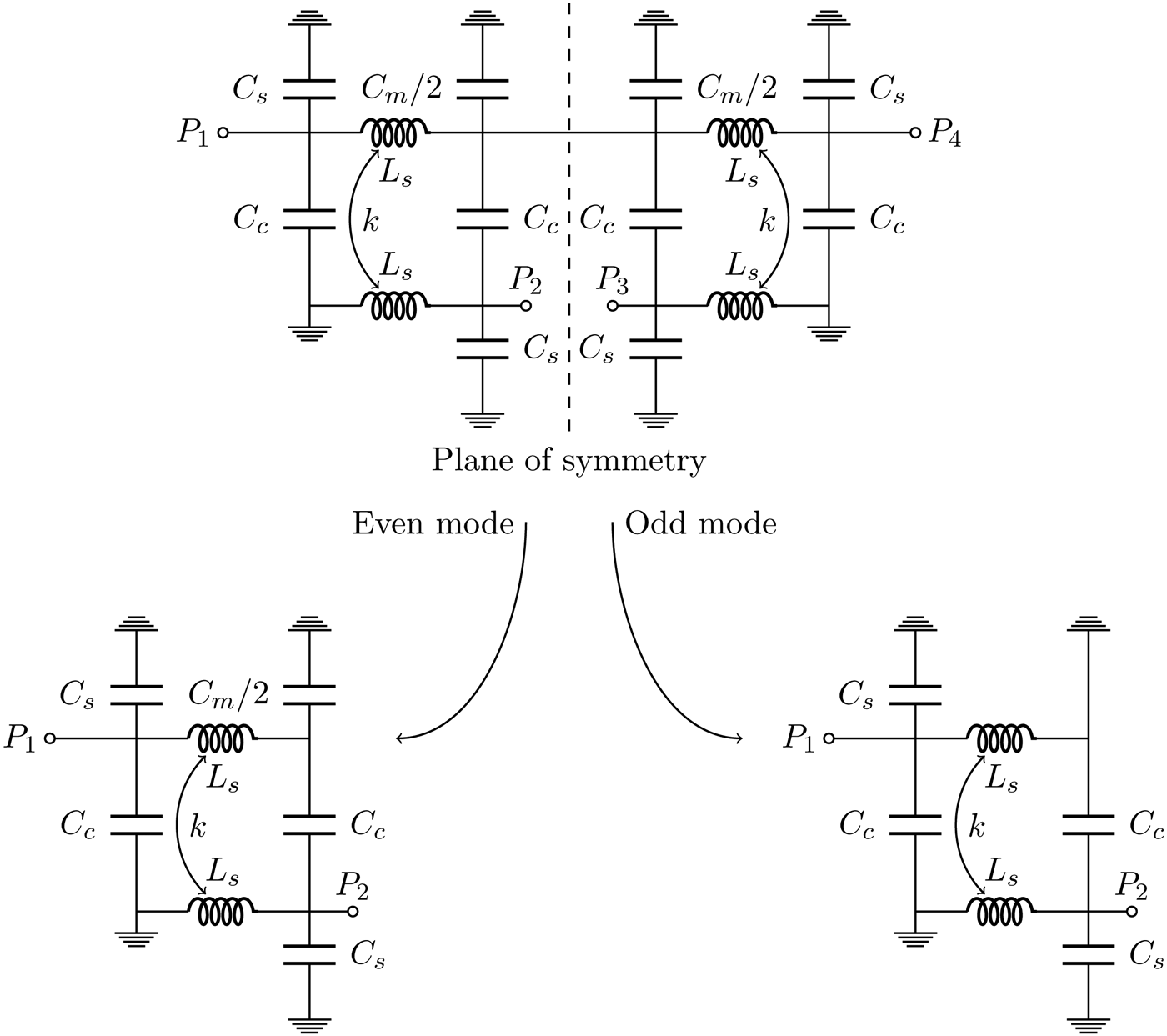
The balun of the double-balanced mixer is implemented in the form of a lumped element Marchand balun. The Marchand balun is chosen owing to its broadband properties. The lumped element implementation allows compact size and straightforward design procedure for good phase and magnitude balance [Reference Johansen and Krozer7, Reference Johansen and Krozer8]. The lumped element implementation uses offset broadside coupled spiral inductors together with capacitors to realize the coupled transmission lines, normally used in Marchand baluns. The schematic of the balun is shown in Fig. 2, where it is depicted as a symmetrical four port, together with the corresponding even- and odd-mode circuits. For normal operation port, four is open circuited.
Fig. 2. Circuit diagram for the lumped Marchand balun, showing it as a symmetrical four port. Normal operation requires P 4 to be open circuited.
For a circuit to behave like an ideal balun, it must have S-parameters given as
 $$S_{21} = - S_{31}\comma \;$$
 $$S_{11} = 0.$$
For a symmetrical four-port circuit, (1) is fulfilled if the fourth port is terminated in an open circuit to give [Reference Ang, Leong and Lee9]
 $$T_{even} = 0\comma \;$$
 $$Z_{in_{even} } + Z_{in_{odd} } = 2Z_{P 1}\comma \;$$
where T even is the transmission coefficient in the even-mode circuit, Z P1 is the system impedance at port 1,  $Z_{in_{even} } $ and
  $Z_{in_{odd} } $ are the input impedance of the even-mode and odd-mode circuits, respectively.
The synthesis of this type of lumped balun is based on the coupled line Marchand balun [Reference Johansen and Krozer7]. Thus the synthesis starts by selecting the even- and odd-mode characteristic impedance of the lines. For a real-valued impedance scaling, α equals Z P2,3/Z P1 the relation giving the even- and odd-mode impedance is [Reference Zhang, Guo, Ong and Chia10]
 $$\displaystyle{1 \over {Z_{0_{odd} } }} - \displaystyle{1 \over {Z_{0_{even} } }} = \displaystyle{1 \over {Z_{P 1} }} \sqrt {\displaystyle{2 \over \alpha }}\comma \;$$
where  $Z_{0_{even} } $ and
  $Z_{0_{odd} } $ are the even- and odd-mode characteristic impedance of the coupled line, respectively.
From the even- and odd-mode characteristic impedance, the circuit parameters for the lumped element balun can be found. This procedure was described in [Reference Johansen and Krozer7] and the design equations are repeated here
 $$L_s = {\displaystyle{{Z_{0_{even} } +\, Z_{0_{odd} } } \over {2\omega }}}\comma \;$$
 $$k = {\displaystyle{{Z_{0_{even} } -\, Z_{0_{odd} } } \over {2\omega L_s }}}\comma \;$$
 $$C_c = {\displaystyle{1 \over {2\omega }}}\left({\displaystyle{1 \over {Z_{0_{odd} } }} - \displaystyle{1 \over {Z_{0_{even} } }}} \right)\comma \;$$
 $$C_s = {\displaystyle{1 \over {\omega Z_{0_{even} } }}}\comma \;$$
where k and C c are the inductive coupling coefficient and the capacitive coupling, respectively, of the coupled spiral pairs. The center capacitors are given as C m = 2C s.
From (5) it is evident that there are several values of  $Z_{0_{odd} } $ and
  $Z_{0_{even} } $, which fulfills the requirement. A higher
  $Z_{0_{odd} } $ gives larger bandwidth, but gives larger inductors in the realization of the lumped element balun, so a trade off between bandwidth and desired balun size must be made. In Figs. 3 and 4, are the design curves plotted for a 50 Ω environment, without scaling.
Fig. 3. Design curves for L s and k as function of  $Z_{0_{odd} } $.
Fig. 4. Design curves for C s, C c and C m as function of  $Z_{0_{odd} } $.
The coupled broadside spiral inductor design is limited in the realization, as it is often not possible to obtain values as dictated by equations (6)–(8). Further investigation of the structure is therefore required to reveal possible solutions or trade offs for this problem. For the even-mode circuit, shown in Fig. 2, the requirement for the transmission coefficient being zero is the same as the Y-parameter Y 21e become zero [Reference Johansen and Krozer8]. Thus, for (1) to be fulfilled we have
 $$Y_{21e} = - \displaystyle{{\lpar 1 - k\rpar s\lpar C_m /2 + C_c \rpar - sC_m /2} \over {s^2 \lpar C_m /2 + C_c \rpar L_s \lpar 1 - k^2 \rpar + 1}} = 0 \Leftrightarrow\comma \;$$
 $$C_m = 2C_c \left({\displaystyle{1 \over k} - 1} \right).$$
This is a nice property as it shows that by careful selection of C m it is possible to obtain good phase and magnitude match even though the coupled spiral is not as specified above. Also note that the match is broadband as it does not depend directly on frequency, but on parameters which ideally should be frequency independent.
The even- and odd-mode impedance can be found, by terminating the even- and odd-mode circuits in Fig. 2 with Z P2, as
 $$\eqalign{&Y_{even} = \displaystyle{1 \over {Z_{even} }} = s\lpar C_s + C_c \rpar + {\displaystyle{{s\left({C_m /2 + C_c } \right)} \over {s^2 \left({C_m /2 + C_c } \right)L_s \lpar 1 - k^2 \rpar + 1}}}\comma \;}$$
 $$\eqalign{&Y_{odd} = \displaystyle{1 \over {Z_{odd} }} = s\lpar C_s + C_c \rpar + {{1 \over {\displaystyle{sL_s }- {\displaystyle{{\mathop {\left({skL_s } \right)}\nolimits^2 } \over {sL_s + {\displaystyle{1 \over {s\left({C_s+C_c } \right)+ Y_{P2} }}}}}}}}}\comma \;}$$
where s = jω is the complex frequency. Note that (12) will always be purely imaginary for real circuits, whereas (13) is a general complex number having a real and a imaginary part. Inserting (12) and (13) into (4) gives the requirement for the perfect input match. Thus, to match to a real source impedance, Z P1, we have Z odd = 1/Y odd = 2Z P1 − Z even, where Z P1 is purely real and Z even is purely imaginary. This corresponds to two real equations in C s. Thus, it is not guaranteed that there exists a C s to fulfill the requirement for arbitrary selection of L s, k and C c.
Even though if the coupled spiral is not as specified by equations (6)–(8), one can try to change C s, to obtain a better match. It is typically possible to find an acceptable match, albeit not perfect.
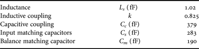
The implemented balun has parameters given by Table 1. The chip area occupied by the balun is 680 µm × 710 µm and a microphotograph is shown in Fig. 5. The S-parameters for the balun is shown in Fig. 6, where simulation results are compared to measurements. It is observed that there is good agreement, in general, between the simulation and experimental results. The largest discrepancy is the S 11 curve where the second resonance behavior is shifted down from 13 to 12 GHz. This shift is probably due to parasitic capacitances not included in the simulation model. At the design frequency a loss of 2.5 dB was measured. The rather high loss is mainly due to the low Q-factor of the inductors. As desired the balun is broadband with a measured 3 dB bandwidth of 6.4 GHz. Figures 7 and 8 show the phase and magnitude imbalances, respectively. Excellent magnitude and phase imbalance of 0.11 dB and 0.7°, respectively, are achieved at the design frequency. A magnitude imbalance better than 0.4 dB and a phase imbalance better than 5°, is achieved over the entire bandwidth of operation, which makes this balun suitable for double-balanced mixer implementation.
Fig. 5. Microphotograph of on chip balun structure. Dimensions are 680 µm × 710 µm.
Fig. 6. Measurements and simulation results for balun S-parameters.
Fig. 7. Measurement and simulation results for phase imbalance.
Fig. 8. Measurement and simulation results for magnitude imbalance.
Table 1. Design parameters for the balun.
B) IF extraction
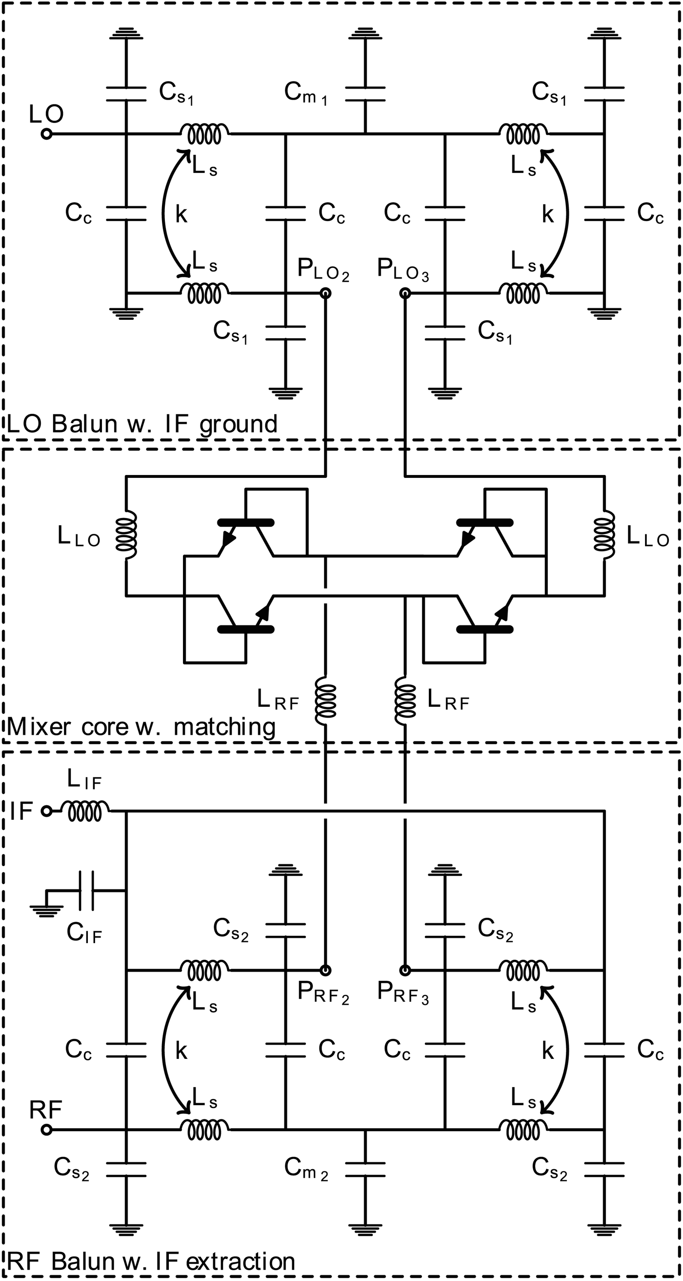
To get an output signal from the mixer it is necessary to have a circuit that allows to extract the IF signal, without disturbing the LO and RF baluns. The IF extraction is achieved by making a DC and low-frequency return path at either the LO or RF port and extract the signal from the other. It is desirable not to have any large signal leaking out of the IF port as this might saturate or cause other unwanted effects in the low-frequency circuitry following the mixer. For this reason, it is chosen to use the balun at the LO port to make the DC and low-frequency return path and the balun at the RF port to extract the IF signal, as the LO-signal can be several magnitudes larger than the RF signal.
Owing to low IF frequency of the mixer together with the grounded parts of the Marchand balun, the IF extraction is quite simple and follows the idea from [Reference Lee, Lin, Hung, Su and Wang11]. The schematic for the IF extraction is the part of Fig. 9 labeled ‘RF balun w. IF extraction’. The DC and low-frequency return path is ensured by the Marchand balun as the inductors L s are seen as a short circuit. To avoid the ground connection in the RF balun, it is blocked by large capacitors which creates an open for the IF signal and a short for the RF signal. It is important to make the IF extraction symmetric as any asymmetry will affect the balun performance. To ensure the symmetry the capacitor C IF is split into three parallel 2 pF capacitors placed after both of the two inductors and in the middle where the IF signal is combined. The small influence on the balun performance from the 2 pF capacitors can be compensated by slightly changing C s2 for matching and C m2 for balance.
Fig. 9. Schematic representation of the full mixer circuit.
C) Mixer core
The mixer core consists of the mixing devices and a matching circuit. Each mixing device is a diode-connected HBT. There are two possible ways to make the diode connections, either by use of the base-emitter or the base-collector pn-junction. The base-emitter junction is the preferred diode junction due to the heavier doping of the n-region of the emitter compared to the collector. Simulations also show that this gives the best behavior, having a 3 dB difference in conversion loss between the two diode connections. To get the double-balanced properties the ring mixer structure is used [Reference Maas3].
Using Harmonic Balance simulations the optimum load conditions are found to be 58 + j106Ω and 50 + j122Ω at 8.5 GHz for the LO and the RF ports, respectively. As a 50Ω match is required it is relatively simple to tune out the reactive part using single series inductors, L RF and L LO. In Fig. 9 the schematic of the mixer core is labeled ‘Mixer core w. matching’.
The mixer has been manufactured using a 0.25 µm SiGe HBT process from IHP. The die size is 2200 µm × 800 µm. A microphotograph of the full mixer is shown in Fig. 10.
Fig. 10. Microphotograph of passive double-balanced mixer. The die size is 2200 µm × 800 µm.
III. EXPERIMENTAL RESULTS
In this section, the experimental results are discussed. The measurements are made on-wafer using a probe station, and simple calibration is used to remove losses in cables and probes. The IF-frequency for all measurements is 100 MHz. The mixer conversion loss and single sideband noise figure is shown in Fig. 11 as a function of frequency, with a fixed LO power of 15 dBm. At the design frequency of 8.5 GHz the conversion loss is 9.8 dB. The noise figure follows the conversion loss as expected. Due to measurement inaccuracy the noise figure is at some points lower than the conversion loss. The 3 dB bandwidth covers more than the entire X-band or more precisely the range from 7 to 12 GHz, thus showing the benefit of using a broadband balun design together with the double-balanced topology.
Fig. 11. Measured conversion loss and single sideband noise figure versus frequency.
In Fig. 12 the conversion loss and noise figure is plotted versus the LO power level, at the design frequency of 8.5 GHz. It is seen that the mixer is not fully saturated at an LO power of 15 dBm which was the limit of the measurement equipment used. To measure the linearity the IF power is measured as a function of the RF power, which is plotted in Fig. 13. Due to equipment limitations the measurement could not be made with a RF power above 12 dBm. At this point there is measured a compression of 0.8 dB. Simulations predict the input referred 1 dB compression point to be at 12.4 dBm. The input referred second-order intercept point (IIP2) is measured with two RF tones at frequencies of 8.4 and 8.413 GHz, giving a second-order product at 13 MHz. Isolators is placed after the signal generators to avoid leakage and intermodulation of the signals before they are applied to the mixer. Attenuation is added to the output of the mixer to avoid measuring the nonlinearity of the spectrum analyzer [Reference Maas12]. From Fig. 13, it can be observed that not only a second order but also a fourth-order phenomenon is observed. It is not possible to distinguish between second- and fourth-order by frequency selection, as a fourth-order term will always be at the same frequency as the second-order term. For weak signals, it is the second-order behavior of the mixer that is dominant, whereas for powers above −5 dBm it is fourth-order which is dominant. This behavior was predicted by the simulations. By extrapolation an IIP2 of 66 dBm is found. This proves that the design gives a high linearity as required.
Fig. 12. Measured conversion loss and single sideband noise figure versus LO power.
Fig. 13. Measured IF power versus RF.
The LO–IF, RF–IF, and LO-RF isolation at the design frequency are 55, 40, and 58 dB, respectively. In Fig. 14, the isolation is plotted versus frequency. In the entire band of operation, the LO–IF, RF–IF, and LO–RF isolation are better than 46, 36, and 36 dB, respectively. The high LO to RF isolation is very important due to self-mixing issues. Self-mixing can give rise to a DC-current through the mixing device, which increases the 1/f noise [Reference Michaelsen, Johansen and Tamborg13].
Fig. 14. Measured LO–IF and RF–IF isolation.
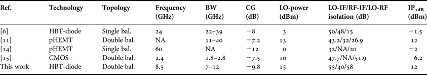
A comparison between this work and passive mixers recently reported in the open literature is presented in Table 2.
Table 2. Comparison between this work and recently reported passive mixers.
IV. CONCLUSION
The design of a passive double-balanced mixer in a 0.25 µm SiGe HBT technology has been presented. The mixer is a direct conversion mixer suitable for use in Doppler radars. The passive mixing element consists of diode-connected HBTs, using the base-emitter pn-junction to realize the mixing diodes. Lumped element Marchand baluns was implemented using offset broadside coupled spiral inductors and capacitors. This gives the possibility of an elegant IF-extraction together with wide bandwidth and good balance.
The lumped element Marchand baluns had an excellent phase and magnitude match of 0.7° and 0.11 dB, respectively. Being broadband they kept a magnitude imbalance better than 0.4 dB and a phase imbalance better than 5° over the entire 3 dB bandwidth of 6.4 GHz. Suffering from the low Q-factor of the inductors, however, they have a rather high loss of 2.5 dB.
The broadband mixer has a 3 dB bandwidth from 7–12 GHz, covering the entire X-band, with a conversion loss of 9.8 dB at the design frequency. It requires a relatively high LO level of 15 dBm for best performance, but has a high linearity with a 1 dB compression point above 12 dBm and IIP 2 at 66 dBm. Good isolation between LO–IF, RF–IF, and LO–RF ports of 55, 40, and 58 dB, respectively, is ensured due to the good balance of the Marchand baluns.
ACKNOWLEDGEMENT
The authors would like to thank the H.C. Ørsteds fond for financial support to cover the cost of chip fabrication.
Vitaliy Zhurbenko received the M.Sc. degree from the Kharkiv National University of Radio Electronics in 2001, and the Ph.D. degree from the Technical University of Denmark in 2008, all in electrical engineering. From November 2000 to Jun 2005, he was a metrology engineer with the Laboratory of Metrology, Kharkiv, Ukraine.
In 2005, he joined the Technical University of Denmark, where he is currently an Associate Professor. His current research interests include microwave and millimeter wave devices and integrated circuits for instrumentation applications; microwave and millimeter wave sensing for biomedical and security applications; microwave imaging and radars; antenna and passive circuit design and characterization.
Kjeld M. Tamborg was born in Kastrup, Denmark in 1966. He received his M.Sc. degree in electronics from the Technical University of Denmark (DTU) in 1990. He was in 1990 hired by Weibel Scientific A/S, Allerød, Denmark, where he is still working. Since 2007 he has been product responsible for the Weibel radar antenna heads and components inside. During his work he has developed micro strip antenna elements, low noise amplifiers, power amplifiers, mixers, oscillators and many other components for X-band radars.
Rasmus S. Michaelsen received the M.Sc. degree in electrical engineering from the Technical University of Denmark in 2010. He is currently working toward the Ph.D. degree together with the technical University of Denmark and Weibel Scientific, Allerød, Denamark. In 2009 he joined Weibel Scientific A/S, designing and testing X-band microwave components, and later as industrial Ph.D student. In 2010 he was on an external stay at Physikalisches Institut, Johann Wolfgang Goethe-Universität, Frankfur am Main, Germany. His current research interests include microwave monolithic integrated circuit (MMIC) design, nonlinear circuits, flicker noise and direct conversion receiver circuits.
Tom K. Johansen received his M.S and Ph.D. degrees in electrical engineering from the Technical University of Denmark, Denmark, in 1999 and 2003, respectively. In 1999 he joined the Electromagnetic Systems group, DTU Elektro, Technical University of Denmark, Denmark, where he is currently an Associate Professor. From September 2001 to March 2002 he was a Visiting scholar at the center for wireless communication, University of San Diego, California, CA. From November 2012 to February 2013 he spent a sabbatical at the Ferdinand Braun Institute (FBH), in Berlin, Germany. His research areas include the modeling of HBT devices, microwave, millimeter-wave and sub-millimeter-wave integrated circuit design.