I. INTRODUCTION
Microstrip antennas are miniaturized antennas and annular ring microstrip antenna (ARMSA) has small dimensions compared with other microstrip shapes resonating at same frequency [Reference Mink1]. Due to the small size, light weight, easy fabrication, and low-profile nature, ARMSA is most widely used for wireless applications [2–10]. In recent years, due to the rapid growth of wireless applications, researchers are paying more attention to design compact and wideband antennas. So there are various techniques to develop compact antenna that have been reported in the literature such as using high relative permittivity dielectric substrate for supporting the patch [Reference Chen, Liu, Chen, Lin, Liu and Duan11], integrating slots in the radiating patch [Reference Iwasaki12], using defected ground plane [Reference Chen13, Reference Gautam and Kanaujia14], slot-loaded patch [Reference Wong, Hsu and Wu15], by inserting slots or spur lines [Reference Lu, Yu and Wong16] at the boundaries or corners of the microstrip patch and shorted pin is also applied for achieving high compactness [Reference Wong, So, Ng, Luk, Chan and Xue17]. In these techniques of reducing the size, the effective current path length increases due to which there is reduction in resonant frequency of the patch resulting compactness in the size of antenna. Microstrip antennas with wide impedance bandwidth may find potential application in wireless communications. In this regard, many techniques have been reported in literature like using multilayer concept or stacked microstrip patch with coaxial feed [Reference Esselle and Verma18–Reference Gupta, Sharma, Kanaujia, Rudra, Misra and Pandey22], L-probe feeding [Reference Lo, Hu, Chan and Luk23, Reference Guo, Luk and Lee24] providing superior bandwidth [Reference Kokotoff, Aberle and Waterhouse25]. L-probe incorporated with patch introduces a capacitance cancelling a few inductance introduced by the probe feed due to thick substrate [Reference Guo, Luk and Lee24].
In this paper, orthogonally slot-loaded ARMSA fed by L-shaped probe is investigated using modal expansion cavity model and circuit theory concept, resulting to the improvement of bandwidth. The effects of the orthogonally slot position at periphery of radiating path are compared with ARMSA to achieve the miniaturization of antenna. Simulated results of radiation characteristics are compared with experimental results. Theoretical results are in good agreement with measured and simulated results. This paper demonstrates the design, simulation, fabrication, and measurement of orthogonally slot-loaded ARMSA fed by L-shaped probe for wireless application. This paper provides scientific knowledge about inserting an orthogonal slot in inner and outer periphery of ARMSA and also delivers the information of parametric study of various parameters on center frequency and bandwidth of the proposed antenna.
II. THEORETICAL ANALYSIS
The geometry of L-probe fed ARMSA is shown in Fig. 1(a). Annular patch is placed on a Rohacell dielectric material (ε r = 1.07) of 8 mm thickness. The inverted L-shaped probe with vertical height of h 1 and horizontal length y 0 is used. The proposed orthogonally slot-loaded L-probe fed ARMSA is shown in Fig. 1(b), which is obtained after cutting the orthogonal slot of 1 mm width and 6 mm of length at inner periphery of annular path of earlier reported structure. Different fabrication stages of the proposed structure are shown in Fig. 1(c)–(f). The proposed structure is analyzed and explained in successive stages as ARMSA, L-probe fed ARMSA, and orthogonal slot-loaded ARMSA in the following section.

Fig. 1. (a) Geometry of L-probe proximity-fed ARMSA, (b) geometry of L-probe proximity-fed ARMSA with orthogonal slot (the drawing is not in the scale) and image of (c) SMA connector on ground plane (d) L-probe (e) ARMSA with slot before fabrication, (f) fabricated ARMSA with slot.
A) ARMSA
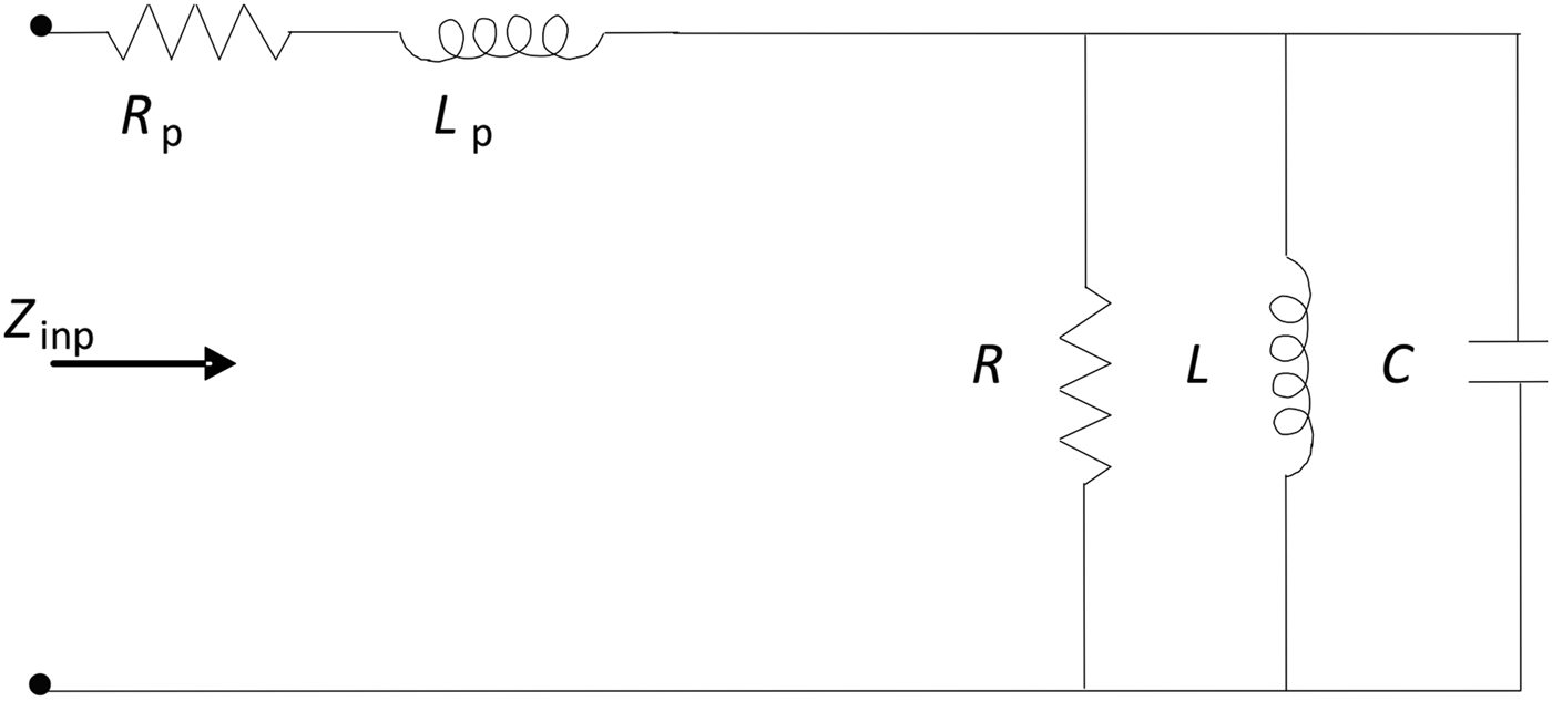
The equivalent circuit of ARMSA can be explained as parallel combination of R, L, and C as shown in Fig. 2. Due to the small value of feed probe resistance R p and inductance L p value in comparison with other component, it can be neglected. Thus, input impedance of ARMSA can be written as
 $${Z_{inp}}=\displaystyle{{R{\omega ^ 2}{L^2}+j{R^2}\lpar \omega L - {\omega ^3}{L^2}C\rpar } \over {{R^2}{{\lpar 1 - {\omega ^2}LC\rpar }^2}+{\omega ^2}{L^2}}}\comma \;$$
where ω = 2πf, and f is the resonant frequency. Equivalent circuit parameters R, L, and C can be expressed as [Reference Ohmine, Sunahara and Matsunaga5].
 $$\eqalign{& C=\displaystyle{{{\rm \pi }\mathop \varepsilon \nolimits_r \mathop \varepsilon \nolimits_0 } \over {\mathop \varepsilon \nolimits_n^ 2 h}} \cr & \quad \displaystyle{{[ {{b^2}\lpar 1 - \lpar {n^2}/{k^2}{b^{2\, }}\rpar \rpar \lcub F\lpar b\rpar {{\rm \rcub }^ 2} - {a^2}\lpar 1 - \lpar {n^2}/{k^2}{b^2}\rpar \rpar \lcub F\lpar a\rpar {{\rm \rcub }^ 2}} ] } \over {{{\lcub F\lpar T\rpar \rcub }^2}}}\comma \; }$$
where k is the resonant wave number, h is the thickness of the dielectric substrate, a and b are the inner and outer radii of ARMSA, ε r is the relative permittivity of the substrate, T is the feed point, and F(b) = J n (bk)Y n ′(ka) − J n (ak)Y n ′(bk); similarly we can get F(a) and F(T) by replacing b with a and T, respectively.

Fig. 2. Equivalent circuit of ARMSA.
The inductance L of the ARMSA is given as
 $$\eqalign{& L=\displaystyle{{\mathop \varepsilon \nolimits_n^ 2 h{\mu _0}} \over {\pi {k^ 2}}} \cr & \quad \displaystyle{{{{\lcub F\lpar T\rpar \rcub }^2}} \over {[ {b^2}\lpar 1 - \lpar {n^2}/{k^2}{b^2}\rpar \rpar {{\lcub F\lpar b\rpar \rcub }^2} - {a^2}\lpar 1 - \lpar {n^2}/{k^2}{b^2}\rpar \rpar {{\lcub F\lpar a\rpar \rcub }^2}] }}\comma \; }$$
where μ
0 is the permeability of free space,
 ${\varepsilon}_{n} = \sqrt 2 $
(for n ≠ 0) and ε
n
= 1 (for n = 0), and the resistance of the ARMSA is calculated as
${\varepsilon}_{n} = \sqrt 2 $
(for n ≠ 0) and ε
n
= 1 (for n = 0), and the resistance of the ARMSA is calculated as
 $$R=\displaystyle{{{Q_0}} \over {\pi fC}}\comma \;$$
where Q 0 is a factor, including dielectric, conductor, and radiation losses.
B) L-probe fed ARMSA
The L-probe proximity fed ARMSA, is shown in Fig. 1(a). A Rohacell foam layer (ε r = 1.07) of thickness 8 mm is used to support the radiating patch above the ground plane. Without L-strip, it is difficult to couple the energy from the microstrip line to the patch as the separation between them is too large therefore an L-probe is introduced. Due to this the spacing between the patch and the feed probe is reduced. Figure 3 represents the equivalent circuit of the L-probe proximity fed ARMSA. The horizontal part of the L-strip of length λ/4 incorporated with the patch provides a capacitance to suppress the inductance introduced by the vertical part of the L-strip. The vertical part of L-probe is equivalent to a series combination of resistance (R s ) and inductance (L s ). The resistance R s is because of finite conductivity of copper used. The expression for the resistance R s and inductance L s are given by [Reference Hoffman26]
 $${L_s}=0.2{h_1}\left\{{\ln \left({\displaystyle{{2{h_1}} \over {{w_s}+{t_s}}}} \right)+0.2235\left({\displaystyle{{{w_s}+{t_{\rm s}}} \over {h1}}} \right)+0.05} \right\}\, \, \lpar \hbox{nH}\rpar \comma \;$$
 $${R_s}=4.13 \times {10^{ - 3}}{h_1}\displaystyle{{\sqrt {f\rho /{\rho _{Cu}}} } \over {{w_s}+{t_s}}}\comma \;$$
where w s is the width of the strip in mm, t s is the thickness of the strip in mm, h 1 is the height of the vertical portion of the L-strip, ρ is the specific resistance of the strip (Ω cm), and ρ Cu is the specific resistance of the copper (1.72106 Ω cm). The horizontal portion of the L-probe and the patch are perfect conductors separated by a finite distance (h 2) which provides a capacitance (C 1) in series with vertical portion of the L-probe and this can be calculated by
 $${C_1}={{{\varepsilon _r}{\varepsilon _0}{y_0}{w_s}} / {{h_2}}}.$$
Also there is a parallel plate capacitance (C s1) between the horizontal part of the L-probe and the ground plane expressed by equation (4) where w s is the width of the L-probe, y 0 is the horizontal length of the L-probe, h 1 is the height of the vertical portion of the L-probe, ε r is the relative permittivity of the material (foam), and ε 0 is the free-space permittivity.
 $${C_{s 1}}={{{\varepsilon _r}{\varepsilon _0}{y_0}{w_s}} / {{h_1}}}.$$

Fig. 3. Equivalent circuit of L-probe proximity-fed ARMSA.
The open end of the L-probe which is under the patch will have fringing fields, which can be considered as a small increase in the length of the L-probe. This effective increase in the length can be calculated as [Reference Hoffman26, Reference Edwards27]
 $${l_e}=\displaystyle{{0.412h\lpar {\varepsilon _e}+0.3\rpar \lpar \lpar {w_s}/h\rpar +0.264\rpar } \over {\lpar {\varepsilon _e} - 0.258\rpar \lpar \lpar {w_s}/h\rpar +0.8\rpar }}\comma \;$$
ε e is the effective dielectric constant of the material and is given by
 $${\varepsilon _e}=\displaystyle{{{\varepsilon _r}+1} \over 2}+\displaystyle{{{\varepsilon _r} - 1} \over 2}{\left({1+\displaystyle{{12H} \over W}} \right)^{ - 0.5}}\comma \;$$
where W = b − a, a and b are the inner and outer radii of the patch antenna, respectively. If l e is the enhancement in effective length due to the fringing fields, then the fringing capacitance (C f ) due to this can be calculated as [Reference Hoffman26, Reference Edwards27]
 $${C_f}={{{l_e}\sqrt {{\varepsilon _e}} } / {c{Z_0}}}.$$
Due to L-probe, a series of combination of resistance (R s ), inductance (L s ), and capacitance (C total ) in series with resonant element of patch as parallel component R, L, and C. Hence, the input impedance (Z in ) of the L-probe proximity-fed ARMSA can be given as
 $${Z_{in}}={R_s}\, +\, j\omega {L_s}+\displaystyle{1 \over {j\omega {C_{total}}}}+{Z_{inp}}\comma \;$$
where C total is the equivalent capacitance because of capacitances C 1, C s1, C f1, and C f2 and is given by [Reference Edwards27]
 $${C_{total}}=\displaystyle{{\lpar {C_1}+2{C_{f2}}\rpar \lpar {C_{s1}}+{C_{f1}}\rpar } \over {\lpar {C_1}+2{C_{f2}}+{C_{s1}}+{C_{f1}}\rpar }}.$$
C) Orthogonally slot-loaded L-probe fed ARMSA
The proposed structure of the L-probe proximity fed ARMSA, with slot is shown in Fig. 1(b). When orthogonal slots are inserted in the L-probe fed annular ring microstrip patch, the total area of the radiating patch is altered. Due to which the value of resistance, inductance, and capacitance has been modified in the circuit. A capacitive (Cc) coupling is taken between slot-loaded patch and without slot-loaded patch, which is shown in Fig. 4.

Fig. 4. Equivalent circuit of L-probe proximity-fed ARMSA with slot.
The input impedance of the loaded slot (Z inm ) can be written as
 $${Z_{inm}}=\displaystyle{ 1 \over {R^{\prime}+j\omega L^{\prime}+{1 / {j\omega C^{\prime}}}}}\comma \;$$
where, R′, L′, and C′ is the equivalent resistance, inductance, and capacitance of slot loaded ARMSA, respectively. Thus, total input impedance (Z int ) of the equivalent circuit is given as
 $$\eqalign{Z_{int} = & R_s+j \omega L_s+\displaystyle{1 \over {j \omega C_{total}}} \cr & +Z_{inm} \{ Z_{inp}+(1/j \omega C_c) \} / \{Z_{inp}+Z_{inm} + (1/j \omega C_c) \}}.$$
III. RESULTS AND DISCUSSIONS
Design parameters of the proposed antenna are listed in Table 1 as given below. The proposed geometry, L-probe proximity fed ARMSA with orthogonally slot cut at the inner periphery of radiating patch is explained in this section. The theoretical results have been calculated using given equations with the help of MATLABTM and the simulated results have been calculated using Ansoft's “High Frequency Structural Simulator” software (HFSSTM). For simulating the structure we have used the wave port mode of excitation for the coaxial feed and the radiation boundary was fixed at a distance of λ/4, being the free space wavelength corresponding to the lowest component of the frequency sweep. Fast sweep mode has been employed to generate the results and a few samples were verified using the results obtained from discrete sweep mode. Good agreement was revealed in each case. Maximum (S-parameter) value of 0.01 was chosen for terminating the adaptive solution and this gives accurate simulation results. Parametric study of |S 11| parameter with frequency for slot width w and slot length l is shown in Figs 5 and 6, respectively. It is observed that by increasing both, the width w of the slot from 0.5 to 1.5 mm and the length l from 5 to 7 mm, the center frequency as well as bandwidth decreases. Parametric study on account of inner and outer radius for |S 11| parameter with frequency is shown in Figs 7 and 8, respectively. From Fig. 7, it is observed that the bandwidth is almost the same for the inner radius values from 8.0 to 9.0 mm and the |S 11| parameter is minimum at first notch at 8.5 mm of the value inner radius. From Fig. 8, it is observed that the bandwidth is maximum for the value of outer radius at b = 17 mm, while |S 11| parameter is increases at first notch with increasing the value of outer radius from 16 to 18 mm. Fig. 9 shows the |S 11| parameter with frequency of the proposed ARMSA for different width w s of L-probe. It is observed that bandwidth of the antenna is approximately same for the value for 0.5 and 1.0 mm, and is greater than for 1.5 mm of slot width, while |S 11| parameter is high for the value of 0.5 mm of slot width. From the analysis of Figs 5–9 optimized value of the parameters such as w, l, a, b, and w s are obtained on the basis of bandwidth and return loss as shown in Table 1. Figure 10 shows the variation of |S 11| parameter with frequency of the proposed ARMSA for different horizontal probe length of L-probe (y 0) keeping other dimensions constant. From Fig. 10 it is observed that the bandwidth of the antenna highly depends on the length of the horizontal section of L-probe under the patch and also found that the maximum impedance bandwidth (37.46%) is for 15 mm of probe length. This is because of the fact that increasing the length of the horizontal section increases the capacitance between the patch and the L-probe and between the patch and ground, which offsets the inductance provided by the vertical portion of the L-probe.

Fig. 5. Variation in the |S 11| parameter with frequency for different slot width (w).

Fig. 6. Variation in the |S 11| parameter with frequency for different slot length (l).

Fig. 7. Variation in the |S 11| parameter with frequency for different inner radius (a).

Fig. 8. Variation in the |S 11| parameter with frequency for different outer radius (b).

Fig. 9. Variation in the |S 11| parameter with frequency for different width of L-probe (w s ).

Fig. 10. Variation in the |S 11| parameter with frequency for different probe length of L-probe (y 0) at h 1 = 7 mm.
Table 1. Antenna design parameters.

Variation in the |S 11| parameter with frequency of the proposed ARMSA for different height of L-probe (h 1) keeping other dimensions constant is shown in Fig. 11. From Fig. 11, it is observed that the maximum impedance bandwidth is obtained for the probe height of 7.0 mm. For enhancing the coupling between vertical section of L-probe and the patch, the gap between them should be small. Therefore the height of vertical portion of the L-probe can be increased to provide good coupling and matching.

Fig. 11. Variation in the |S 11| parameter with frequency for different height of L-probe (h 1) at y 0 = 15 mm.
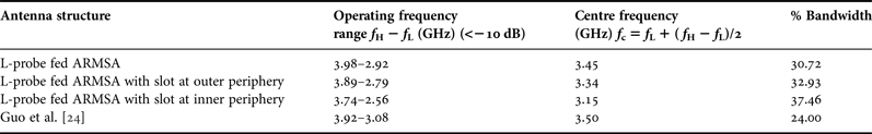
Variation in |S 11| parameter with frequency for the different antenna geometry is shown in Fig. 12. It is observed that the ARMSA without slots resonates at 3.45 GHz with 30.72% bandwidth (|S 11| < −10 dB), whereas ARMSA with slot at outer periphery of radiating patch is resonating at 3.34 GHz with 32.93%. This reduction of 0.11 GHz in the resonance frequency is due to the increase in the average path length of the current existing on radiating patch, this effect can be viewed in Fig. 13. Figure 13(a) shows the current path of ARMSA without slot and Fig. 13(b) shows the current path of slot loaded at outer periphery of radiating patch. It can be visualized that after loading of the slot, current path is not straightway as in the case of without slot. Bandwidth is enhanced due to the reduction in capacitance between radiating patch and ground plane and also due to slot loading in radiating patch reduces the total area, hence less stored energy and low-quality factor resulting wider bandwidth [Reference Chew28]. When slot is loaded at inner periphery of radiating patch as shown in Fig. 13(c) then ARMSA resonates at lowest frequency as 3.15 GHz with maximum impedance bandwidth as 37.46%. Comparison of bandwidth and central frequency for all antenna structure and previously reported L-probe proximity fed ARMSA without slot in [Reference Guo, Luk and Lee24] are listed in Table 2. By observing this table, it is found that the bandwidth enhancement of the proposed structure is 13.46% from the previously reported structure. Further reduction in resonance frequency of antenna is due to the increase in the average path length of current.

Fig. 12. Variation in the |S 11| parameter with frequency of ARMSA without slot, slot at outer periphery, and slot at inner periphery of the radiating patch.

Fig. 13. Simulated surface current distribution of (a) ARMSA without slot at 3.45 GHz, (b) ARMSA with slot in the outer periphery at 3.34 GHz, and (c) ARMSA with slot in the inner periphery at 3.15 GHz.
Table 2. Comparison of bandwidth and central frequency for different antenna structures.

Increment in impedance bandwidth of ARMSA with slot at inner periphery of radiating patch is due to the reduction in fringing capacitance between L-probe and radiating patch also with reduction in capacitance between radiating patch and ground plane. From Fig. 13, it is also observed that all the three structures are resonating in TM11 mode, which can be analyzed from the pattern of current direction, and only one half-wave length exists in X- and Y-axis.
The far-field radiation pattern of the proposed ARMSA for both E- and H-planes at resonant frequency 3.15 GHz are shown in Figs 14 and 15, respectively. It is observed that simulated results of both E- and H-planes are in good agreement with the experimental results. The half-power (−3 dB) beam-width of the antenna is 96° (from −48º to 48º), and the cross-polarization of E-plane is below −13 dB. It should be noted that the H-plane cross-polarization level is quite low.

Fig. 14. E-plane radiation pattern at resonance frequency 3.15 GHz

Fig. 15. H-plane radiation pattern at resonant frequency 3.15 GHz.
Variation in antenna gain with frequency of the proposed antenna is shown in Fig. 16. Measured result of antenna gain is in close agreement with simulated results. It is observed that the gain of the antenna is stable over the entire impedance bandwidth.

Fig. 16. Variation in gain with frequency of the proposed antenna.
IV. CONCLUSION
Orthogonally slot-loaded ARMSA with L-probe feeding is presented. The design realizes an impedance bandwidth of about 37.46% (|S 11| < −10 dB) at resonant frequency 3.15 GHz with 15 mm length of horizontal L-probe and 7 mm height of L-probe from the ground plane. Miniaturization of the proposed structure is about 10% and broadening bandwidth of about 13.46% from the earlier reported [Reference Guo, Luk and Lee24] structure. The proposed antenna resonates at 3.5 GHz which may be utilized for Wi-MAX applications.
 Anil Kumar Singh was born in Jamalpur, Mirzapur, UP, India on July 10, 1976. He received his M.Tech. Degree in Instrumentation and Control Engineering from NITTTR Chandigarh, India in 2011. He is currently working toward the Ph.D. degree on Some Study on Annular Ring Microstrip Antenna from Electronics Engineering Department, Indian School of Mines (ISM), Dhanbad, India. He joined the Department of Electronics and Instrumentation Engineering, Institute of Engineering and Technology, M. J. P. Rohilkhand University, Bareilly as a Lecturer in 2002. He has published more than 20 papers in national and international journals and conferences. His current research interest includes design and analysis of microstrip antennas. He is a graduate student member of IEEE.
 Ravi Kumar Gangwar received his B.Tech. degree in Electronics and Communication Engineering from U.P. Technical University, and Ph.D. degree in Electronics Engineering from the Indian Institute of Technology, Banaras Hindu University (IIT-BHU), Varanasi, India in 2006 and 2011, respectively. He is currently working as an Assistant Professor in the Department of Electronics Engineering, Indian School of Mines, Dhanbad, India. He has authored or coauthored over 40 research papers in international/national journals/conference proceedings. His research interest includes Dielectric Resonator Antenna, Microstrip Antenna, Metamaterial, and Bio-Electromagnetics. He is a Member of the Antenna and Propagation Society and Communication Society, Institute of Electrical and Electronics Engineers (IEEE), USA. He is a reviewer of Progress in Electromagnetic Research, International Journal of Electronics, International Journal of Microwave and Wireless Technology, Wireless Personnel Communication, Indian Journal of Radio & Space Physics (IJRSP), Indian Journal of Pure & Applied Physics (IJPAP) journals.
 Binod Kumar Kanaujia is currently working as an Associate Professor in the Department of Electronics & Communication Engineering in Ambedkar Institute of Advanced Communication Technologies & Research (formerly Ambedkar Institute of Technology), Geeta Colony, Delhi. Dr. Kanaujia joined this institute as an Assistant Professor in 2008 through selection by Union Public Service Commission, New Delhi, India and served in various key portfolios, i.e. Head of Department, In-charge Central Library, Head of Office, etc. Before joining this institute he served in the M.J.P. Rohilkhand University, Bareilly, India as Reader in the Department of Electronics & Communication Engineering and also as Head of the Department. He has been an active member of Academic Council and Executive Council of the M.J.P. Rohilkhand University and played a vital role in academic reforms. Prior, to his career in academics, Dr. Kanaujia worked as Executive Engineer in the R&D division of M/s UPTRON India Ltd. Dr. Kanaujia completed his B.Tech. in Electronics Engineering from KNIT Sultanpur, India in 1994. He did his M.Tech. and Ph.D. in 1998 and 2004, respectively from the Department of Electronics Engineering, Indian Institute of Technology Banaras Hindu University, Varanasi, India. He has been awarded Junior Research Fellowship by UGC Delhi in the year 2001–2002 for his outstanding work in the electronics field. He has keen research interest in design and modeling of microstrip antenna, dielectric resonator antenna, left-handed metamaterial microstrip antenna, shorted microstrip antenna, ultra wideband antennas, reconfigurable, and circular polarized antenna for wireless communication. He has been credited to publish more than 105 research papers with more than 200 citations with h-index of ten in peer-reviewed journals and conferences. He supervised 45 M.Tech. and three Ph.D. research scholars in the field of Microwave Engineering. He is a reviewer of several journals of international repute, i.e. IET Microwaves, Antennas & Propagation, IEEE Antennas and Wireless Propagation Letters, Wireless Personal Communications, Journal of Electromagnetic Wave and Application, Indian Journal of Radio and Space Physics, IETE Technical Review, International Journal of Electronics, International Journal of Engineering Science, IEEE Transactions on Antennas and Propagation, AEU-International Journal of Electronics and Communication, International Journal of Microwave and Wireless Technologies, etc. Dr. Kanaujia has successfully executed four research projects sponsored by several agencies of Government of India, i.e. DRDO, DST, AICTE, and ISRO. He is also a member of several academic and professional bodies, i.e. IEEE, Institution of Engineers (India), Indian Society for Technical Education, and The Institute of Electronics and Telecommunication Engineers of India.